EP1158564B1 - An electron spin analyzer - Google Patents
An electron spin analyzer Download PDFInfo
- Publication number
- EP1158564B1 EP1158564B1 EP01109500A EP01109500A EP1158564B1 EP 1158564 B1 EP1158564 B1 EP 1158564B1 EP 01109500 A EP01109500 A EP 01109500A EP 01109500 A EP01109500 A EP 01109500A EP 1158564 B1 EP1158564 B1 EP 1158564B1
- Authority
- EP
- European Patent Office
- Prior art keywords
- electron
- electrode
- accelerating electrode
- scattered
- electron spin
- Prior art date
- Legal status (The legal status is an assumption and is not a legal conclusion. Google has not performed a legal analysis and makes no representation as to the accuracy of the status listed.)
- Expired - Lifetime
Links
- 0 CC1CC(*)CCC1 Chemical compound CC1CC(*)CCC1 0.000 description 1
Images


Classifications
-
- G—PHYSICS
- G01—MEASURING; TESTING
- G01N—INVESTIGATING OR ANALYSING MATERIALS BY DETERMINING THEIR CHEMICAL OR PHYSICAL PROPERTIES
- G01N24/00—Investigating or analyzing materials by the use of nuclear magnetic resonance, electron paramagnetic resonance or other spin effects
-
- H—ELECTRICITY
- H01—ELECTRIC ELEMENTS
- H01J—ELECTRIC DISCHARGE TUBES OR DISCHARGE LAMPS
- H01J37/00—Discharge tubes with provision for introducing objects or material to be exposed to the discharge, e.g. for the purpose of examination or processing thereof
- H01J37/252—Tubes for spot-analysing by electron or ion beams; Microanalysers
-
- H—ELECTRICITY
- H01—ELECTRIC ELEMENTS
- H01J—ELECTRIC DISCHARGE TUBES OR DISCHARGE LAMPS
- H01J2237/00—Discharge tubes exposing object to beam, e.g. for analysis treatment, etching, imaging
- H01J2237/04—Means for controlling the discharge
- H01J2237/047—Changing particle velocity
- H01J2237/0473—Changing particle velocity accelerating
- H01J2237/04735—Changing particle velocity accelerating with electrostatic means
-
- H—ELECTRICITY
- H01—ELECTRIC ELEMENTS
- H01J—ELECTRIC DISCHARGE TUBES OR DISCHARGE LAMPS
- H01J2237/00—Discharge tubes exposing object to beam, e.g. for analysis treatment, etching, imaging
- H01J2237/245—Detection characterised by the variable being measured
- H01J2237/24507—Intensity, dose or other characteristics of particle beams or electromagnetic radiation
- H01J2237/24557—Spin polarisation (particles)
Definitions
- This invention relates to an electron spin analyzer, particularly, to an electron spin analyzer which is preferably usable for a high effective electron spin analyzer such as an electronic material analyzer and a magnetic material surface analyzer.
- a conventional electron spin analyzer tends to be enlarged for detecting scattered electrons effectively.
- a Mott spin analyzer is required to detect scattered electrons over the wide scattered angle range of 95-145 degrees, and thus, the scattered electron detector thereof must be enlarged.
- An enlargement of an apparatus is not desired in view of installment space and operationality, and thus, the electron spin analyzer is also being required to be downsized.
- the conventional electron spin analyzer is downsized with maintaining the structure, it can not detect the scattered electrons effectively.
- the present invention provides, in one aspect, an electron spin analyzer having all the features of claim 1.
- the present invention provides an electron spin analyzer having all the features of claim 4.
- Preferred embodiments of the analyzer according to the invention are given in the dependent sub-claims.
- the scattered electron detector provided as part of the electron spin analyzer on the outer surface of the accelerating electrode has a correcting electrode therein.
- the scattered electron detector may be arranged so as to be shifted by 100 - 140 degrees, except 120 degrees, from an introducing direction of electrons to be scattered.
- the inventors has intensely studied to prevent the degradation of the detection sensitivity of scattered electrons even if the electron spin analyzer is downsized.
- the electron spin analyzer is so formed that its hemisphere accelerating electrode is composed of an inner accelerating electrode and an outer accelerating electrode, and its inner introducing inlet formed at the inner accelerating electrode has a larger size than that of its outer introducing inlet formed at the outer accelerating electrode, according to the first aspect of the present invention.
- electron beams to be introduced can be converged onto a scattering target in high density, and thus, the convergence degree of the scattered electrons is increased.
- the scattered electrons can be detected effectively, and the detection sensitivity can be increased.
- the inner opening formed at the inner accelerating electrode to introduce the scattered electrons into a scattered electron detector is larger than the outer opening formed at the outer accelerating electrode to do ditto. Therefore, the convergence degree of the scattered electrons is increased, so that the scattered electrons can be detected effectively at the scattered electron detector and the detection sensitivity of the analyzer can be increased. Furthermore, by providing a correcting electrode to capture the scattered electrons for the scattered electron detector, the convergence degree of the scattered electrons can be increased. Therefore, the detection sensitivity of the analyzer can be increased.
- the inventors have also figured out that, although the distribution of scattered electrons becomes maximum in the shifted direction from the introducing direction of the electron by 120 degrees in a normal size electron spin analyzer, it becomes maximum in the different direction from the shifted direction in a downsized electron spin analyzer.
- the electron spin analyzer of the present invention By fabricating the electron spin analyzer of the present invention so that the scattered electron detector is positioned at the maximum distribution of the scattered electrons, the detection sensitivity of the scattered electrons can be increased.
- Fig. 1 is a cross sectional view showing a preferred embodiment of the electron spin analyzer of the present invention.
- the introducing direction of electrons is designated by an arrow.
- the electron spin analyzer depicted in Fig. 1 has an electron beam-generating apparatus 1, a hemisphere accelerating electrode composed of an outer accelerating electrode 2 and an inner accelerating electrode 3 which are positioned so as to oppose the electron beam-discharging hole 1A of the electron beam-generating apparatus 1.
- the outer and inner accelerating electrodes 2 and 3 are supported by an electrode supporting member 6.
- a pair of scattered electron detectors 4, 4 are provided on the outer surface of the outer accelerating electrode 2 so as to be symmetrical for the introducing direction of electrons, and a scattering target 5, supported by a supporter 13 attached to the electrode supporting member 6, is provided inside the outer and inner accelerating electrodes 2 and 3.
- An outer introducing inlet 14 and an inner introducing inlet 15 are formed at the outer accelerating electrode 2 and the inner accelerating electrode 3, respectively, for introducing electron beams from the electron beam-generating apparatus 1 onto the scattering target 5. Then, outer openings 8, 8 and inner openings 7, 7 are formed at the outer accelerating electrode 2 and the inner accelerating electrode 3, respectively, for introducing the scattered electrons from the scattering target 5 into the scattered electron detectors 4, 4.
- the inner introducing inlet 15 has a larger size than that of the outer introducing inlet 14. Concretely, it is preferable that the aperture angle ⁇ of the inner introducing inlet 15 is larger than the aperture angle ⁇ of the outer introducing inlet 14 by 0.1-5 degrees. Thereby, as mentioned above, the introduced electrons can be converged onto the scattering target in high density, and thus, the detection sensitivity of the scattered electrons can be increased.
- each of the inner openings 7, 7 has a larger size than that of each of the outer openings 8, 8.
- the aperture angle ⁇ of the inner opening 7 is larger than the aperture ⁇ of the outer opening 8 by 1.0-5 degrees.
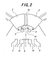
- Fig. 2 is an enlarged view showing a part of the electron spin analyzer shown in Fig. 1 near the outer introducing inlet 14 and the inner introducing inlet 15.
- the edge portions 2a, 2b and 3a, 3b, which are opposed one another, of the outer and inner introducing inlets 14 and 15 formed at the outer and inner accelerating electrodes 2 and 3 have curvatures, respectively. Therefore, the convergence degree of the introduced electrons can be much increased, and thus, the detection sensitivity of the scattered electrons can be much increased.
- each of the edge portions 2a and 2b of the outer introducing inlet 14, formed at the outer accelerating electrode 2 has a curvature radius R1 of 0.5-2 mm.
- each of the edge portions 3a and 3b of the inner introducing inlet 15, formed at the inner accelerating electrode 3 has a curvature radius r1 of 0.5-2 mm.
- Fig. 3 is an enlarged view showing a part of the electron spin analyzer shown in Fig. 1 near the inner opening 7 and the outer opening 8.
- the edge portions 2A, 2B and 3A, 3B, which are opposed one another, of the outer and inner openings 8 and 7 formed at the outer and inner accelerating electrodes 2 and 3 have curvatures, respectively. Therefore, the convergence degree of the introduced electrons can be much increased, and thus, the detection sensitivity of the scattered electrons can be much increased.
- each of the edge portions 2A and 2B of the outer opening 8, formed at the outer accelerating electrode 2 has a curvature radius R2 of 0.5-2 mm.
- the edge portions 3A and 3B of the inner opening 7, formed at the inner accelerating electrode 3 has a curvature radius r2 of 0.5-2 mm.
- the scattered electron detector 4 has a detector 10, a grid 11 in front of the detector 10, and a correcting electrode 9 in both sides of the detector 10 and the grid 11, which are enclosed by a shield 12.
- the scattered electrons to be introduced into the scattered electron detectors 4,4 are converged by the correcting electrode 9 provided in the detector 8, and thus, the large amount of the scattered electrons can arrive at the detector 10 through the grid 11.
- the electron spin analyzer depicted in Fig. 1 can have high sensitivity.
- the correcting electrode 9 is provided for converging the scattered electrons to be introduced into the scattered electron detector 4, it is preferably composed of an electrostatic lens.
- the electrostatic lens a unipotential lens and a bipotential lens may be exemplified.
- the electrostatic lens has a cylindrical shape for enhancing the convergence degree of the scattered electrons.
- the scattered electron detectors 4, 4 are positioned in the shifted directions from the introducing direction of electrons by an angle ⁇ of 100-140 degrees except 120 degrees, preferably 115-125 degrees except 120 degrees. As mentioned above, since the distribution of the scattered electrons becomes maximum at the above positions when the electron spin analyzer is downsized, the detection sensitivity of the scattered electrons can be enhanced if the scattered electron detectors are arranged at the above positions.
- each part constituting the electron spin analyzer depicted in Fig. 1 may be made of a well known material to persons skilled in the art.
- the electron spin analyzer shown in Fig. 1 has the above-mentioned pair of scattering electron detectors which are symmetrical for the introducing direction of electrons. Therefore, spin component in one direction from among the scattered electrons can be measured.
- an additional pair of scattered electron detectors are arranged in the direction perpendicular to this paper so that each of all the four scattered electron detectors can satisfy four-fold symmetric condition, spin components in two directions from among the scattered electrons can be measured.
- the electron spin detector can be downsized without the degradation of the detection sensitivity of the scattered electrons.
Landscapes
- Chemical & Material Sciences (AREA)
- Analytical Chemistry (AREA)
- Physics & Mathematics (AREA)
- High Energy & Nuclear Physics (AREA)
- Health & Medical Sciences (AREA)
- Life Sciences & Earth Sciences (AREA)
- Biochemistry (AREA)
- General Health & Medical Sciences (AREA)
- General Physics & Mathematics (AREA)
- Immunology (AREA)
- Pathology (AREA)
- Analysing Materials By The Use Of Radiation (AREA)
- Measurement Of Radiation (AREA)
- Electron Tubes For Measurement (AREA)
Description
- This invention relates to an electron spin analyzer, particularly, to an electron spin analyzer which is preferably usable for a high effective electron spin analyzer such as an electronic material analyzer and a magnetic material surface analyzer.
- A conventional electron spin analyzer tends to be enlarged for detecting scattered electrons effectively. For example, a Mott spin analyzer is required to detect scattered electrons over the wide scattered angle range of 95-145 degrees, and thus, the scattered electron detector thereof must be enlarged.
An enlargement of an apparatus is not desired in view of installment space and operationality, and thus, the electron spin analyzer is also being required to be downsized. However, if the conventional electron spin analyzer is downsized with maintaining the structure, it can not detect the scattered electrons effectively. - An article "Simple, compact, medium-energy Mott polarization analyzer" by L.G. Gray et al., published in Review of Scientific Instruments 55(1), January 1984, pages 88 - 91, discloses a spherical retarding Mott polarization analyzer featuring a hemispherical electrode structure including a radially inner electrode and a radially outer electrode. Apertures are formed in the electrodes to allow an electron beam to pass through the electrodes from a beam source to a scattering target and from there to an electron detector. The apertures in the outer electrode are of larger size than the corresponding apertures in the inner electrode.
It is an object of the present invention, to provide an electron spin analyzer which can detect scattered electrons efficiently even if it is downsized. To achieve this object, the present invention provides, in one aspect, an electron spin analyzer having all the features of claim 1. In another aspect, the present invention provides an electron spin analyzer having all the features ofclaim 4. Preferred embodiments of the analyzer according to the invention are given in the dependent sub-claims.
In a preferred embodiment, the scattered electron detector provided as part of the electron spin analyzer on the outer surface of the accelerating electrode has a correcting electrode therein. The scattered electron detector may be arranged so as to be shifted by 100 - 140 degrees, except 120 degrees, from an introducing direction of electrons to be scattered.
The inventors has intensely studied to prevent the degradation of the detection sensitivity of scattered electrons even if the electron spin analyzer is downsized. At last, they found the following fact: That is, the electron spin analyzer is so formed that its hemisphere accelerating electrode is composed of an inner accelerating electrode and an outer accelerating electrode, and its inner introducing inlet formed at the inner accelerating electrode has a larger size than that of its outer introducing inlet formed at the outer accelerating electrode, according to the first aspect of the present invention. As a result, electron beams to be introduced can be converged onto a scattering target in high density, and thus, the convergence degree of the scattered electrons is increased.
According to the first aspect, the scattered electrons can be detected effectively, and the detection sensitivity can be increased. - Moreover, according to the second aspect of the present invention, the inner opening formed at the inner accelerating electrode to introduce the scattered electrons into a scattered electron detector is larger than the outer opening formed at the outer accelerating electrode to do ditto. Therefore, the convergence degree of the scattered electrons is increased, so that the scattered electrons can be detected effectively at the scattered electron detector and the detection sensitivity of the analyzer can be increased.
Furthermore, by providing a correcting electrode to capture the scattered electrons for the scattered electron detector, the convergence degree of the scattered electrons can be increased. Therefore, the detection sensitivity of the analyzer can be increased. - Then, the inventors have also figured out that, although the distribution of scattered electrons becomes maximum in the shifted direction from the introducing direction of the electron by 120 degrees in a normal size electron spin analyzer, it becomes maximum in the different direction from the shifted direction in a downsized electron spin analyzer. By fabricating the electron spin analyzer of the present invention so that the scattered electron detector is positioned at the maximum distribution of the scattered electrons, the detection sensitivity of the scattered electrons can be increased.
- The first and second aspects may be independently employed, but if they are combined, the detection sensitivity of the scattered electrons can be extremely increased.
For better understanding of the present invention, reference is made to the attached drawings, wherein - Fig. 1 is a cross sectional view showing an embodiment in the electron spin analyzer of the present invention,
- Fig. 2 is an enlarged sectional view showing a part of the electron spin analyzer shown in Fig. 1, and
- Fig. 3 is also an enlarged sectional view showing a part of the electron spin analyzer shown in Fig. 1.
- This invention will be described in detail with reference to figures. Fig. 1 is a cross sectional view showing a preferred embodiment of the electron spin analyzer of the present invention.
Herein, the introducing direction of electrons is designated by an arrow. - The electron spin analyzer depicted in Fig. 1 has an electron beam-generating apparatus 1, a hemisphere accelerating electrode composed of an outer accelerating
electrode 2 and an inner acceleratingelectrode 3 which are positioned so as to oppose the electron beam-discharging hole 1A of the electron beam-generating apparatus 1. The outer and inner acceleratingelectrodes electrode supporting member 6. A pair ofscattered electron detectors electrode 2 so as to be symmetrical for the introducing direction of electrons, and ascattering target 5, supported by asupporter 13 attached to theelectrode supporting member 6, is provided inside the outer and inner acceleratingelectrodes - An outer introducing
inlet 14 and an inner introducinginlet 15 are formed at the outer acceleratingelectrode 2 and the inner acceleratingelectrode 3, respectively, for introducing electron beams from the electron beam-generating apparatus 1 onto thescattering target 5. Then,outer openings inner openings electrode 2 and the inner acceleratingelectrode 3, respectively, for introducing the scattered electrons from thescattering target 5 into thescattered electron detectors - The inner introducing
inlet 15 has a larger size than that of the outer introducinginlet 14. Concretely, it is preferable that the aperture angle α of the inner introducinginlet 15 is larger than the aperture angle β of the outer introducinginlet 14 by 0.1-5 degrees. Thereby, as mentioned above, the introduced electrons can be converged onto the scattering target in high density, and thus, the detection sensitivity of the scattered electrons can be increased. - Moreover, each of the
inner openings outer openings inner opening 7 is larger than the aperture φ of theouter opening 8 by 1.0-5 degrees. Thereby, as mentioned above, the scattered electrons can be converged in high density, and thus, the detection sensitivity of the scattered electrons can be increased through the increase of the detection degree of the scattered electrons at the scattered electron detectors. - Fig. 2 is an enlarged view showing a part of the electron spin analyzer shown in Fig. 1 near the outer introducing
inlet 14 and the inner introducinginlet 15.
As is apparent from Fig. 2, theedge portions inlets electrodes - On account of the same reason, it is desired that each of the
edge portions inlet 14, formed at the outer acceleratingelectrode 2, has a curvature radius R1 of 0.5-2 mm.
Similarly, it is desired that each of theedge portions inlet 15, formed at the inner acceleratingelectrode 3, has a curvature radius r1 of 0.5-2 mm. - Fig. 3 is an enlarged view showing a part of the electron spin analyzer shown in Fig. 1 near the
inner opening 7 and theouter opening 8.
As is apparent from Fig. 3, theedge portions inner openings electrodes - On account of the same reason, it is desired that each of the
edge portions outer opening 8, formed at the outer acceleratingelectrode 2, has a curvature radius R2 of 0.5-2 mm.
Similarly, it is desired that theedge portions 3A and 3B of theinner opening 7, formed at the inner acceleratingelectrode 3, has a curvature radius r2 of 0.5-2 mm. - The
scattered electron detector 4 has adetector 10, agrid 11 in front of thedetector 10, and a correctingelectrode 9 in both sides of thedetector 10 and thegrid 11, which are enclosed by ashield 12. The scattered electrons to be introduced into thescattered electron detectors electrode 9 provided in thedetector 8, and thus, the large amount of the scattered electrons can arrive at thedetector 10 through thegrid 11. As a result, the electron spin analyzer depicted in Fig. 1 can have high sensitivity. - Since the correcting
electrode 9 is provided for converging the scattered electrons to be introduced into thescattered electron detector 4, it is preferably composed of an electrostatic lens. As the electrostatic lens, a unipotential lens and a bipotential lens may be exemplified. Moreover, it is desired that the electrostatic lens has a cylindrical shape for enhancing the convergence degree of the scattered electrons. - The
scattered electron detectors - Herein, each part constituting the electron spin analyzer depicted in Fig. 1 may be made of a well known material to persons skilled in the art.
Moreover, the electron spin analyzer shown in Fig. 1 has the above-mentioned pair of scattering electron detectors which are symmetrical for the introducing direction of electrons. Therefore, spin component in one direction from among the scattered electrons can be measured. Furthermore, not shown in Fig. 1, if an additional pair of scattered electron detectors are arranged in the direction perpendicular to this paper so that each of all the four scattered electron detectors can satisfy four-fold symmetric condition, spin components in two directions from among the scattered electrons can be measured. - Although the present invention was described in detail with reference to the above example, this invention is not limited to the above disclosure and every kind of variation and modification may be made without departing from the scope of the present invention.
- As explained above, according to the present invention, the electron spin detector can be downsized without the degradation of the detection sensitivity of the scattered electrons.
Claims (9)
- An electron spin analyzer comprising an electron beam-generating apparatus (1), a hemisphere accelerating electrode (2, 3) opposing to the electron beam-discharging hole (1A) of the electron beam-generating apparatus (1), an electrode supporter (6) to support the accelerating electrode (2, 3), a scattered electron detector (4) provided on the outer surface of the accelerating electrode (2, 3), and a scattering target (5) provided on the electrode supporter (6) inside the accelerating electrode (2, 3), the accelerating electrode (2, 3) having a double structure composed of an inner accelerating electrode (3) with an inner introducing inlet (15) and an outer accelerating electrode (2) with an outer introducing inlet (14), characterized in that the inner introducing inlet (15) has a larger size than the outer introducing inlet (14).
- An electron spin analyzer as defined in claim 1, wherein the aperture angle (α) of the inner introducing inlet (15) with respect to the scattering target (5) is larger than that (β) of the outer introducing inlet (14) by 0.1-5 degrees.
- An electron spin analyzer as defined in claim 1 or 2, wherein the edge portions (2a, 2B, 3a, 3B) of the inner and the outer introducing inlets (14, 15), which are opposed one another, have curvatures, respectively.
- An electron spin analyzer comprising an electron beam-generating apparatus (1), a hemisphere accelerating electrode (2, 3) opposing to the electron beam-discharging hole (1A) of the electron beam-generating apparatus (1), an electrode supporter (6) to support the accelerating electrode (2, 3), a scattered electron detector (4) provided on the outer surface of the accelerating electrode (2, 3), and a scattering target (5) provided on the electrode supporter (6) inside the accelerating electrode (2, 3), the accelerating electrode (2, 3) having a double structure composed of an inner accelerating electrode (3) with an inner opening (7) and an outer accelerating electrode (2) with an outer opening (8), the inner and outer openings (7, 8) adapted to introduce, during use, scattered electrons from the scattering target (5) into the scattered electron detector (4), characterized in that the inner opening (7) has a larger size than the outer opening (8).
- An electron spin analyzer as defined in claim 4, wherein the aperture angle (θ) of the inner opening (7) with respect to the scattering target (5) is larger than that (φ) of the outer opening (8) by 0,1 - 5 degrees.
- An electron spin analyzer as defined in claim 4 or 5, wherein the edge portions (2A, 2B, 3A, 3B) of the inner and the outer openings (7, 8), which are opposed one another, have curvatures, respectively.
- An electron spin analyzer as defined in one of claims 1 to 6, wherein the scattered electron detector (4) has a correcting electrode (9) therein.
- An electron spin analyzer as defined in claim 7, wherein the correcting electrode (9) is composed of an electrostatic lens.
- An electron spin analyzer as defined in one of claims 1 to 8, wherein the scattered electron detector (4) is arranged so as to be shifted from an introducing direction of electrons to be introduced by 100 - 140 degrees, except 120 degrees.
Applications Claiming Priority (2)
| Application Number | Priority Date | Filing Date | Title |
|---|---|---|---|
| JP2000133700A JP3757263B2 (en) | 2000-05-02 | 2000-05-02 | Electron spin analyzer |
| JP2000133700 | 2000-05-02 |
Publications (3)
| Publication Number | Publication Date |
|---|---|
| EP1158564A2 EP1158564A2 (en) | 2001-11-28 |
| EP1158564A3 EP1158564A3 (en) | 2005-06-15 |
| EP1158564B1 true EP1158564B1 (en) | 2007-06-20 |
Family
ID=18642135
Family Applications (1)
| Application Number | Title | Priority Date | Filing Date |
|---|---|---|---|
| EP01109500A Expired - Lifetime EP1158564B1 (en) | 2000-05-02 | 2001-04-25 | An electron spin analyzer |
Country Status (7)
| Country | Link |
|---|---|
| US (1) | US6639218B2 (en) |
| EP (1) | EP1158564B1 (en) |
| JP (1) | JP3757263B2 (en) |
| KR (1) | KR100456368B1 (en) |
| CN (1) | CN1322004A (en) |
| DE (1) | DE60128985T2 (en) |
| HK (1) | HK1040821A1 (en) |
Families Citing this family (10)
| Publication number | Priority date | Publication date | Assignee | Title |
|---|---|---|---|---|
| JP3383842B2 (en) | 2000-04-28 | 2003-03-10 | 北海道大学長 | Scattering target holding mechanism and electron spin analyzer |
| DE10339404B4 (en) * | 2003-04-02 | 2009-03-05 | Gst Mbh | Arrangement for the analysis of the electron spin polarization in parallel imaging electron microscopes |
| US7375802B2 (en) * | 2005-08-04 | 2008-05-20 | Lockheed Martin Corporation | Radar systems and methods using entangled quantum particles |
| DE102005045622B4 (en) * | 2005-09-23 | 2009-04-30 | GST Gesellschaft für systembezogene Technologieentwicklung mbH | Methods and arrangements for detecting electron spin polarization |
| US7985952B2 (en) * | 2007-03-05 | 2011-07-26 | Hitachi, Ltd. | Charged particle spin polarimeter, microscope, and photoelectron spectroscope |
| JP5222712B2 (en) * | 2008-12-22 | 2013-06-26 | 株式会社日立製作所 | Electron spin detector, spin-polarized scanning electron microscope and spin-resolved photoelectron spectrometer using the same |
| CN104345331B (en) * | 2013-07-24 | 2017-04-19 | 中国科学院上海微系统与信息技术研究所 | image type electron spin analyzer |
| US11402445B2 (en) | 2015-10-27 | 2022-08-02 | Hosein Majlesi | Electron intrinsic spin analyzer |
| CN109470732B (en) * | 2017-09-07 | 2020-11-24 | 中国科学院上海微系统与信息技术研究所 | an electronic optical system |
| CN109470731B (en) * | 2017-09-07 | 2020-10-20 | 中国科学院上海微系统与信息技术研究所 | An image-type electron spin analyzer |
Family Cites Families (12)
| Publication number | Priority date | Publication date | Assignee | Title |
|---|---|---|---|---|
| DE2646394C2 (en) * | 1976-10-14 | 1986-12-11 | Kernforschungsanlage Jülich GmbH, 5170 Jülich | Device for determining the degree of spin polarization of an electron beam |
| JPS6017846A (en) | 1983-07-08 | 1985-01-29 | Hitachi Ltd | Electron spin polarization detector |
| JPS60177539A (en) | 1984-02-24 | 1985-09-11 | Hitachi Ltd | Scanning electron microscope |
| JPS60105152A (en) | 1984-10-05 | 1985-06-10 | Hitachi Ltd | Scanning electron microscope |
| US4760254A (en) * | 1985-06-07 | 1988-07-26 | Pierce Daniel T | Apparatus and method for electron spin polarization detection |
| JPH0786897B2 (en) | 1987-05-15 | 1995-09-20 | シャープ株式会社 | Card reader |
| JP2680018B2 (en) * | 1988-02-26 | 1997-11-19 | 株式会社日立製作所 | Spin polarization detector |
| JPH04206427A (en) | 1990-11-30 | 1992-07-28 | Hitachi Ltd | Spin detector |
| US5444243A (en) * | 1993-09-01 | 1995-08-22 | Hitachi, Ltd. | Wien filter apparatus with hyperbolic surfaces |
| JP3302569B2 (en) | 1996-07-09 | 2002-07-15 | 科学技術振興事業団 | Method and apparatus for measuring electron spin polarization |
| JP3383842B2 (en) | 2000-04-28 | 2003-03-10 | 北海道大学長 | Scattering target holding mechanism and electron spin analyzer |
| JP4020296B2 (en) * | 2000-12-21 | 2007-12-12 | キヤノン株式会社 | Ionic conduction structure, secondary battery and method for producing them |
-
2000
- 2000-05-02 JP JP2000133700A patent/JP3757263B2/en not_active Expired - Lifetime
-
2001
- 2001-04-25 EP EP01109500A patent/EP1158564B1/en not_active Expired - Lifetime
- 2001-04-25 DE DE60128985T patent/DE60128985T2/en not_active Expired - Fee Related
- 2001-04-26 US US09/843,445 patent/US6639218B2/en not_active Expired - Fee Related
- 2001-04-27 KR KR10-2001-0022898A patent/KR100456368B1/en not_active Expired - Fee Related
- 2001-04-30 CN CN01116778A patent/CN1322004A/en active Pending
-
2002
- 2002-03-19 HK HK02102080.5A patent/HK1040821A1/en unknown
Non-Patent Citations (1)
| Title |
|---|
| None * |
Also Published As
| Publication number | Publication date |
|---|---|
| US20020003213A1 (en) | 2002-01-10 |
| DE60128985T2 (en) | 2007-10-18 |
| HK1040821A1 (en) | 2002-06-21 |
| CN1322004A (en) | 2001-11-14 |
| KR100456368B1 (en) | 2004-11-10 |
| JP3757263B2 (en) | 2006-03-22 |
| US6639218B2 (en) | 2003-10-28 |
| DE60128985D1 (en) | 2007-08-02 |
| EP1158564A3 (en) | 2005-06-15 |
| KR20010106195A (en) | 2001-11-29 |
| JP2001319611A (en) | 2001-11-16 |
| EP1158564A2 (en) | 2001-11-28 |
Similar Documents
| Publication | Publication Date | Title |
|---|---|---|
| USRE33275E (en) | Electron Spectrometer | |
| US20250232951A1 (en) | Particle beam system | |
| TWI301992B (en) | High current density particle beam system | |
| TWI603363B (en) | Secondary charged particle detection system, charged particle beam device, and method of detecting secondary charged particles | |
| US5559337A (en) | Plasma ion source mass analyzing apparatus | |
| US6639218B2 (en) | Electron spin analyzer | |
| US6730907B1 (en) | Charged particle device | |
| EP0470299A1 (en) | Energy filter for charged particle beam apparatus | |
| EP2654068A1 (en) | Switchable multi perspective detector, optics therefore and method of operating thereof | |
| KR102872217B1 (en) | Multi-particle beam system with contrast correction lens system | |
| US5422486A (en) | Scanning electron beam device | |
| JPH0736321B2 (en) | Spectrometer-objective lens system for quantitative potential measurement | |
| JP2018006339A (en) | Scanning electron microscope | |
| US20040211913A1 (en) | Objective lens arrangement for use in a charged particle beam column | |
| JP4662053B2 (en) | Scanning electron microscope with multiple detectors and multiple detector-based imaging method | |
| JP2009507328A (en) | Reflectron | |
| JPH1064464A (en) | Detection element objective lens device | |
| JPS6329436A (en) | Charged particle optical system with astigmation correction means | |
| KR20000034962A (en) | Dual-mode detection of charged particles | |
| US6407388B1 (en) | Corpuscular beam device | |
| JPH08510596A (en) | Particle optics with secondary electron deflection unit | |
| JP6646463B2 (en) | Signal charged particle deflector, signal charged particle detection system, charged particle beam device, and method of detecting signal charged particle beam | |
| EP0996960A1 (en) | Cathode ray tube having a deflection unit | |
| TW201941247A (en) | Apparatus and method for measuring energy spectrum of reflected electrons | |
| EP0754348B1 (en) | Colour display tube comprising an in-line electron gun |
Legal Events
| Date | Code | Title | Description |
|---|---|---|---|
| PUAI | Public reference made under article 153(3) epc to a published international application that has entered the european phase |
Free format text: ORIGINAL CODE: 0009012 |
|
| 17P | Request for examination filed |
Effective date: 20010904 |
|
| AK | Designated contracting states |
Kind code of ref document: A2 Designated state(s): AT BE CH CY DE DK ES FI FR GB GR IE IT LI LU MC NL PT SE TR |
|
| AX | Request for extension of the european patent |
Free format text: AL;LT;LV;MK;RO;SI |
|
| PUAL | Search report despatched |
Free format text: ORIGINAL CODE: 0009013 |
|
| RIC1 | Information provided on ipc code assigned before grant |
Ipc: 7G 01T 1/32 B Ipc: 7H 01J 37/244 B Ipc: 7H 01J 37/295 A |
|
| AK | Designated contracting states |
Kind code of ref document: A3 Designated state(s): AT BE CH CY DE DK ES FI FR GB GR IE IT LI LU MC NL PT SE TR |
|
| AX | Request for extension of the european patent |
Extension state: AL LT LV MK RO SI |
|
| AKX | Designation fees paid |
Designated state(s): DE FR GB |
|
| GRAP | Despatch of communication of intention to grant a patent |
Free format text: ORIGINAL CODE: EPIDOSNIGR1 |
|
| GRAS | Grant fee paid |
Free format text: ORIGINAL CODE: EPIDOSNIGR3 |
|
| GRAA | (expected) grant |
Free format text: ORIGINAL CODE: 0009210 |
|
| AK | Designated contracting states |
Kind code of ref document: B1 Designated state(s): DE FR GB |
|
| REG | Reference to a national code |
Ref country code: GB Ref legal event code: FG4D |
|
| REF | Corresponds to: |
Ref document number: 60128985 Country of ref document: DE Date of ref document: 20070802 Kind code of ref document: P |
|
| ET | Fr: translation filed | ||
| PLBE | No opposition filed within time limit |
Free format text: ORIGINAL CODE: 0009261 |
|
| STAA | Information on the status of an ep patent application or granted ep patent |
Free format text: STATUS: NO OPPOSITION FILED WITHIN TIME LIMIT |
|
| 26N | No opposition filed |
Effective date: 20080325 |
|
| GBPC | Gb: european patent ceased through non-payment of renewal fee |
Effective date: 20080425 |
|
| PG25 | Lapsed in a contracting state [announced via postgrant information from national office to epo] |
Ref country code: DE Free format text: LAPSE BECAUSE OF NON-PAYMENT OF DUE FEES Effective date: 20081101 |
|
| REG | Reference to a national code |
Ref country code: FR Ref legal event code: ST Effective date: 20081231 |
|
| PG25 | Lapsed in a contracting state [announced via postgrant information from national office to epo] |
Ref country code: FR Free format text: LAPSE BECAUSE OF NON-PAYMENT OF DUE FEES Effective date: 20080430 |
|
| PG25 | Lapsed in a contracting state [announced via postgrant information from national office to epo] |
Ref country code: GB Free format text: LAPSE BECAUSE OF NON-PAYMENT OF DUE FEES Effective date: 20080425 |