EP1158327A2 - Arrayed waveguide grating (AWG) on an integrated optics chip - Google Patents
Arrayed waveguide grating (AWG) on an integrated optics chip Download PDFInfo
- Publication number
- EP1158327A2 EP1158327A2 EP01304153A EP01304153A EP1158327A2 EP 1158327 A2 EP1158327 A2 EP 1158327A2 EP 01304153 A EP01304153 A EP 01304153A EP 01304153 A EP01304153 A EP 01304153A EP 1158327 A2 EP1158327 A2 EP 1158327A2
- Authority
- EP
- European Patent Office
- Prior art keywords
- light
- substrate
- waveguide
- coupling section
- input waveguide
- Prior art date
- Legal status (The legal status is an assumption and is not a legal conclusion. Google has not performed a legal analysis and makes no representation as to the accuracy of the status listed.)
- Withdrawn
Links
Images


Classifications
-
- G—PHYSICS
- G02—OPTICS
- G02B—OPTICAL ELEMENTS, SYSTEMS OR APPARATUS
- G02B6/00—Light guides; Structural details of arrangements comprising light guides and other optical elements, e.g. couplings
- G02B6/10—Light guides; Structural details of arrangements comprising light guides and other optical elements, e.g. couplings of the optical waveguide type
- G02B6/12—Light guides; Structural details of arrangements comprising light guides and other optical elements, e.g. couplings of the optical waveguide type of the integrated circuit kind
- G02B6/12007—Light guides; Structural details of arrangements comprising light guides and other optical elements, e.g. couplings of the optical waveguide type of the integrated circuit kind forming wavelength selective elements, e.g. multiplexer, demultiplexer
- G02B6/12009—Light guides; Structural details of arrangements comprising light guides and other optical elements, e.g. couplings of the optical waveguide type of the integrated circuit kind forming wavelength selective elements, e.g. multiplexer, demultiplexer comprising arrayed waveguide grating [AWG] devices, i.e. with a phased array of waveguides
- G02B6/12014—Light guides; Structural details of arrangements comprising light guides and other optical elements, e.g. couplings of the optical waveguide type of the integrated circuit kind forming wavelength selective elements, e.g. multiplexer, demultiplexer comprising arrayed waveguide grating [AWG] devices, i.e. with a phased array of waveguides characterised by the wavefront splitting or combining section, e.g. grooves or optical elements in a slab waveguide
-
- G—PHYSICS
- G02—OPTICS
- G02B—OPTICAL ELEMENTS, SYSTEMS OR APPARATUS
- G02B6/00—Light guides; Structural details of arrangements comprising light guides and other optical elements, e.g. couplings
- G02B6/10—Light guides; Structural details of arrangements comprising light guides and other optical elements, e.g. couplings of the optical waveguide type
- G02B6/12—Light guides; Structural details of arrangements comprising light guides and other optical elements, e.g. couplings of the optical waveguide type of the integrated circuit kind
- G02B6/12007—Light guides; Structural details of arrangements comprising light guides and other optical elements, e.g. couplings of the optical waveguide type of the integrated circuit kind forming wavelength selective elements, e.g. multiplexer, demultiplexer
- G02B6/12009—Light guides; Structural details of arrangements comprising light guides and other optical elements, e.g. couplings of the optical waveguide type of the integrated circuit kind forming wavelength selective elements, e.g. multiplexer, demultiplexer comprising arrayed waveguide grating [AWG] devices, i.e. with a phased array of waveguides
- G02B6/12019—Light guides; Structural details of arrangements comprising light guides and other optical elements, e.g. couplings of the optical waveguide type of the integrated circuit kind forming wavelength selective elements, e.g. multiplexer, demultiplexer comprising arrayed waveguide grating [AWG] devices, i.e. with a phased array of waveguides characterised by the optical interconnection to or from the AWG devices, e.g. integration or coupling with lasers or photodiodes
- G02B6/12021—Comprising cascaded AWG devices; AWG multipass configuration; Plural AWG devices integrated on a single chip
-
- G—PHYSICS
- G02—OPTICS
- G02B—OPTICAL ELEMENTS, SYSTEMS OR APPARATUS
- G02B6/00—Light guides; Structural details of arrangements comprising light guides and other optical elements, e.g. couplings
- G02B6/10—Light guides; Structural details of arrangements comprising light guides and other optical elements, e.g. couplings of the optical waveguide type
- G02B6/12—Light guides; Structural details of arrangements comprising light guides and other optical elements, e.g. couplings of the optical waveguide type of the integrated circuit kind
- G02B6/13—Integrated optical circuits characterised by the manufacturing method
-
- G—PHYSICS
- G02—OPTICS
- G02B—OPTICAL ELEMENTS, SYSTEMS OR APPARATUS
- G02B6/00—Light guides; Structural details of arrangements comprising light guides and other optical elements, e.g. couplings
- G02B6/24—Coupling light guides
- G02B6/26—Optical coupling means
- G02B6/30—Optical coupling means for use between fibre and thin-film device
Definitions
- This invention relates to a chip for separating light into different wavelengths, it's fabrication and implementation.
- An optical fiber is often used for transmitting light signals over long distances. Light of different wavelengths can be mixed and transmitted through a single optical fiber. For purposes of signal processing, it may be necessary to separate the light into different wavelengths at a receiving end. Many devices have been developed for separating light into different wavelengths. One such device is described in U.S. Patent No. 5,913,000.
- the invention provides a chip for separating light into different wavelengths.
- the chip includes a substrate, an input waveguide, an optical arrangement, and a plurality of output waveguides.
- the substrate has first and second edge sections.
- the input waveguide is formed on the substrate and has an end for providing light thereto located at the first edge section.
- the input waveguide extends from the first end thereof in a first direction.
- the optical arrangement receives the light from the input waveguide and separates the light into a pattern of light of different wavelengths.
- the output waveguides are formed on the substrate.
- Each output waveguide receives light of a respective wavelength from the optical arrangement and transmits the light.
- Each output waveguide has an end, from which the light is transmitted, located at the second edge section.
- Each output waveguide extends to the second end thereof in a second direction.
- the second direction is different from the first direction.
- the second direction may be at an angle of at least 90° with respect to the first direction.
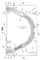
- FIG. 1 of the accompanying drawings illustrates a chip 10 for separating a light into different wavelengths.
- the chip includes a substrate 12 on which an optical structure 14 is formed.
- the optical structure 14 maybe made of silicon dioxide or another material through which light can be channeled.
- the optical material is deposited on the substrate and etched to leave a plurality of input waveguides 16, a primary coupling section 18, a plurality of grating waveguides 20, a secondary coupling section 22, and a plurality of output waveguides 24.
- Each input waveguide 16 has a first end 28, a length 30, and a second end 32.
- the second ends 32 of the input waveguides 16 terminate against the primary coupling section 18.
- Each grating waveguide 20 has a first end 34 originating on a side of the primary coupling section 18 opposing the input waveguides 16, a length 36, and a second end 38.
- the grating waveguides 20 are curved so that outer ones of the grating waveguides 20 have longer lengths 38 than inner ones of the grating waveguides 20.
- the second ends 38 of the grating waveguides 20 terminate against one side of the secondary coupling section 22.
- Each output waveguide 24 has a first end 40 originating at a side of the secondary coupling section 22 opposing the grating waveguide 20, a length 42, and a second end 44.
- the input waveguides 16 extend in a first direction 48 from the first ends 28 thereof.
- the output waveguides 24 extend in a second direction 50 to the second ends 44 thereof.
- the second direction 50 is different from the first direction 48 by an angle 52 of about 180°.
- each optical structure 14 has a generally "U"-shape because the first and second directions 48 and 50 oppose one another.
- a "U"-shape allows for a smaller chip 10 to be made and, accordingly, a higher packing density of chips 10 on the wafer 56.
- the chips 10 are separated from one another in a subsequent sawing operation.
- each chip 10 has a rectangular shape with two opposing long edges 60A and 60B and two opposing short edges 62A and 62B.
- the first end 28 of the input waveguides 16 and the second ends 44 of the output waveguides 24 are all located in line on one of the long edges 60A.
- the long edge 60A with the ends 28 and 44 thereon is subsequently polished by a polishing surface of a polisher 64.
- the polisher 64 moves over a first, edge section 66 to polish the ends 28 and then along the edge 60A and then over a second edge section 68 of the edge 60A where the ends 44 are located.
- Both edge sections 66 and 68 are polished in a single polishing operation wherein the polisher 64 moves in a straight line along the edge 60A. Because only the edge 60A has to be polished, polishing efficiency is increased. Moreover, because the polisher 64 moves in a straight line, there is more uniformity of polishing between the first edge section 66 and the second edge section 68.
- a defect will occur when the first edge section 66 is polished, with a corresponding effect on how the optical structure 14 functions.
- the defect will however be duplicated on the second edge section 68 and the effect on how the optical structure 14 functions due to the defect of the first edge section 66 may be canceled by the defect at the second edge section 68.
- light can be provided to the first end 28 of one of the input waveguides 16 and be transmitted through the length 30 to the second end 32 of the input waveguide 16.
- the light is then diffused from the second end 32 of the input waveguide 16 through the primary coupling section 18 over a wider dispersion area 70.
- the light then enters the first end 34 of each grating waveguide 20 and transmits through the length 36 of the grating waveguides 20 to the second ends 38 thereof.
- the light then radiates and disperses from the second ends 38 through the secondary coupling section 22 over a wider interference area 72. Because of differences in the lengths 36 of the grating waveguides 20, an interference pattern of light of different wavelengths is created over the interference area 72.
- the first ends 40 of the output waveguides are located at different locations of the interference area 72 so that light of a respective wavelength is provided thereto. Light of a respective wavelength transmits through the length 72 of each output waveguide 24 to the second ends 44 of the output waveguides 24.
- the primary coupling section 18, the grating waveguides 20, and the secondary coupling section 22 thus form an optical arrangement 74 which separates light provided to one of the input waveguides 16 into light of different wavelengths which is provided to the output waveguides 24. Further details of how the chip 10 functions are detailed in U.S. patent No. 5,913,000 which is hereby incorporated by reference.
- Figure 3 illustrates a circuit board layout 80 including a printed circuit board 82 and the chip 10 of Figure 1.
- Optical couplings 84 are connected to the input and output waveguides 16 and 24.
- Optical fiber leads 86 extend from the coupling 84.
- the chip 10 is located at a comer of the printed circuit board 82. The location of the chip 10 is made possible because the input and output waveguides 16 and 24 do not terminate at opposing edges of the chip 10.
- the angle see reference numeral 52 in Figure 1
- the angle may be about 90° and terminating ends of input and output waveguides 16 and 24 maybe located on edges which are at right angles to one another. Such a chip would still fit into a comer of a printed circuit board.
Landscapes
- Physics & Mathematics (AREA)
- Engineering & Computer Science (AREA)
- Microelectronics & Electronic Packaging (AREA)
- General Physics & Mathematics (AREA)
- Optics & Photonics (AREA)
- Optical Integrated Circuits (AREA)
- Optical Couplings Of Light Guides (AREA)
Abstract
Description
Claims (10)
- A chip for separating light into different wavelengths, comprising:a substrate having first and second edge sections;an input waveguide, on the substrate, having an end for providing light thereto located at the first edge section, the input waveguide extending from the end thereof in a first direction;an optical arrangement which receives the light form the input waveguide and separating the light into a pattern of light of different wavelengths; anda plurality of output waveguides, on the substrate, each receiving light of a respective wavelength from the optical arrangement and transmitting the light, each having an end, from which the light is transmitted, located at the second 11 edge section, and each extending to the end thereof in a second direction which 12 is different from the first direction.
- A chip according to claim 1 wherein the second direction is at an angle of 2 at least 90° with respect to the first direction.
- A chip according to claim 1 wherein the second direction is about 180° with respect to the first direction.
- A chip according to claim 1 wherein the first and second edge sections both fall and extend in a single line.
- A chip for separating light into different wavelengths, comprising:a substrate having first and second edge sections;an input waveguide, on the substrate, having a first end for providing input light thereto, the first end being located a the first edge section, a length through which the light transmits, and a second end thereof in a first direction;a primary coupling section, on the substrate, into which the light from the input waveguide radiates and disperses through the primary coupling section over a wider dispersion area;a plurality of grating waveguides, on the substrate, each having a first end at a different location of the dispersion area for providing the dispersed light thereto, a length through which the light transmits, and a second end from which the light radiates;a secondary coupling section, on the substrate, into which light from each grating waveguide radiates and disperses through the secondary coupling section over a wider interference area, the grating waveguides having different lengths so that an interference pattern of light of different wavelengths is created over the interference area; anda plurality of output waveguides, on the substrate, each having a first end located at a different location of the interference area so that light of a respective wavelength is provided thereto, a length through which the light transmits, and a second end from which the light is transmitted, the second end being located at the second edge section, the output waveguide extending to the second end thereof in a second direction which is different from the first direction.
- A chip according to claim 5 wherein the second direction is at an angle of at least 90° with respect to the first direction.
- A chip according to claim 5 wherein the second direction is about 180° with respect to the first direction.
- A chip according to claim 5 wherein the first and second edge sections both fall in a single line.
- A method for making a chip for separating light into different wavelengths, comprising:forming an input waveguide, a primary coupling section, a plurality of grating waveguides, a secondary coupling section, and a plurality of output waveguides on a wafer;severing the wafer into a substrate having a first and second edge sections which are both located in a single line, the input waveguide having a first end for providing input light thereto, the first end being located at the first edge section, a length through which the light transmits, and a second end from which the light radiates, the input waveguide extending from the first end thereof in a first direction, light from the input waveguide radiating into the primary coupling section and dispersing through the primary coupling section over a wider dispersion area, each grating waveguide having a first end at a different location of the dispersion area for providing the dispersed light thereto, a length through which the light transmits, and a second end from which the light radiates, light from each grating waveguide radiating into the secondary coupling section and dispersing through the secondary coupling section over a wider interference area, the grating waveguides having different lengths so that an interference pattern of light of different wavelenghts is created over the interference area, each output waveguide having a first end located at a different location of the interference area so that light of a respective wavelength is provided thereto, a length through which the light transmits, and a second end from which the light is transmitted, the second end being located at the second edge section; andpolishing the first and second edge sections along the line.
- A method according to claim 9 wherein the first and second edge sections are both polished with the same polisher without the polisher leaving the substrate.
Applications Claiming Priority (2)
| Application Number | Priority Date | Filing Date | Title |
|---|---|---|---|
| US578796 | 1995-12-26 | ||
| US09/578,796 US6456758B1 (en) | 2000-05-23 | 2000-05-23 | Chip for separating light into different wavelengths |
Publications (2)
| Publication Number | Publication Date |
|---|---|
| EP1158327A2 true EP1158327A2 (en) | 2001-11-28 |
| EP1158327A3 EP1158327A3 (en) | 2004-03-17 |
Family
ID=24314348
Family Applications (1)
| Application Number | Title | Priority Date | Filing Date |
|---|---|---|---|
| EP01304153A Withdrawn EP1158327A3 (en) | 2000-05-23 | 2001-05-08 | Arrayed waveguide grating (AWG) on an integrated optics chip |
Country Status (4)
| Country | Link |
|---|---|
| US (1) | US6456758B1 (en) |
| EP (1) | EP1158327A3 (en) |
| CN (1) | CN1325034A (en) |
| CA (1) | CA2344534A1 (en) |
Cited By (3)
| Publication number | Priority date | Publication date | Assignee | Title |
|---|---|---|---|---|
| EP1279979A3 (en) * | 2001-07-24 | 2004-06-16 | Samsung Electronics Co., Ltd. | Packaged device for optical waveguide element |
| EP1241498A3 (en) * | 2001-03-16 | 2004-09-29 | Nortel Networks Limited | Multiplexer based on arrayed waveguide grating (AWG) |
| WO2004090594A1 (en) * | 2003-04-10 | 2004-10-21 | Lambda Crossing Ltd. | Planar optical component for coupling light to a high index waveguide, and method of its manufacture |
Families Citing this family (2)
| Publication number | Priority date | Publication date | Assignee | Title |
|---|---|---|---|---|
| JP2002014245A (en) * | 2000-06-28 | 2002-01-18 | Nec Corp | Array waveguide diffraction grating, optical coupling and branching system using array waveguide diffraction grating and optical coupling and branching device |
| US7382953B1 (en) * | 2007-02-09 | 2008-06-03 | Gemfire Corporation | Folded AWG architecture |
Family Cites Families (9)
| Publication number | Priority date | Publication date | Assignee | Title |
|---|---|---|---|---|
| US5523879A (en) * | 1991-04-26 | 1996-06-04 | Fuji Xerox Co., Ltd. | Optical link amplifier and a wavelength multiplex laser oscillator |
| US5440416A (en) * | 1993-02-24 | 1995-08-08 | At&T Corp. | Optical network comprising a compact wavelength-dividing component |
| US5913000A (en) * | 1995-12-29 | 1999-06-15 | Doerr; Christopher Richard | Method and apparatus for guiding optical signals |
| US5745616A (en) * | 1996-11-27 | 1998-04-28 | Lucent Technologies Inc. | Waveguide grating router and method of making same having relatively small dimensions |
| WO1998032196A1 (en) * | 1997-01-17 | 1998-07-23 | Tellium, Inc. | Integrated multi-wavelength transmitter |
| JP3436937B2 (en) * | 1997-02-14 | 2003-08-18 | 日本電信電話株式会社 | Optical waveguide circuit and manufacturing method, and optical waveguide circuit module having the optical waveguide circuit |
| FR2770307B1 (en) * | 1997-10-27 | 1999-11-26 | Commissariat Energie Atomique | PHASE ARRAY OR PHASAR DEVICE AND MANUFACTURING METHOD THEREOF |
| GB2334343A (en) * | 1998-02-13 | 1999-08-18 | Northern Telecom Ltd | Optical waveguide multiplexer/demultiplexer with diffraction gratings embracing one another |
| EP1026526A1 (en) * | 1999-02-02 | 2000-08-09 | Corning Incorporated | Athermalized polymer overclad integrated planar optical waveguide device and its manufacturing method |
-
2000
- 2000-05-23 US US09/578,796 patent/US6456758B1/en not_active Expired - Fee Related
-
2001
- 2001-05-03 CA CA002344534A patent/CA2344534A1/en not_active Abandoned
- 2001-05-08 EP EP01304153A patent/EP1158327A3/en not_active Withdrawn
- 2001-05-23 CN CN01119179A patent/CN1325034A/en active Pending
Cited By (4)
| Publication number | Priority date | Publication date | Assignee | Title |
|---|---|---|---|---|
| EP1241498A3 (en) * | 2001-03-16 | 2004-09-29 | Nortel Networks Limited | Multiplexer based on arrayed waveguide grating (AWG) |
| EP1279979A3 (en) * | 2001-07-24 | 2004-06-16 | Samsung Electronics Co., Ltd. | Packaged device for optical waveguide element |
| US6839492B2 (en) | 2001-07-24 | 2005-01-04 | Samsung Electronics Co., Ltd | Packaging device for optical waveguide element |
| WO2004090594A1 (en) * | 2003-04-10 | 2004-10-21 | Lambda Crossing Ltd. | Planar optical component for coupling light to a high index waveguide, and method of its manufacture |
Also Published As
| Publication number | Publication date |
|---|---|
| CA2344534A1 (en) | 2001-11-23 |
| US6456758B1 (en) | 2002-09-24 |
| CN1325034A (en) | 2001-12-05 |
| EP1158327A3 (en) | 2004-03-17 |
Similar Documents
| Publication | Publication Date | Title |
|---|---|---|
| US10429582B1 (en) | Waveguide-to-waveguide couplers with multiple tapers | |
| CN114063211B (en) | Edge coupler with partially etched back taper | |
| CN114252954B (en) | Heterogeneous optical power splitter/combiner | |
| US10444433B1 (en) | Waveguides including a patterned dielectric layer | |
| EP0256388B1 (en) | Optical multi/demultiplexer | |
| US20220229250A1 (en) | Edge couplers in the back-end-of-line stack of a photonics chip | |
| US12147075B2 (en) | Back-end-of-line edge couplers with a tapered grating | |
| CN114690310B (en) | Edge coupler including fluted film | |
| US11808995B2 (en) | Edge couplers with non-linear tapers | |
| CN114384630B (en) | Optical power splitter including nonlinear waveguide taper | |
| US6456758B1 (en) | Chip for separating light into different wavelengths | |
| CN114594545B (en) | Optical power splitter with side wall element | |
| CN115113326B (en) | Optical coupler for ridge-to-rib waveguide core transition | |
| US11378749B2 (en) | Optical power splitters with a multiple-level arrangement | |
| US12422632B2 (en) | Systems and methods for passively-aligned optical waveguide edge-coupling | |
| US11719895B1 (en) | Spot-size converters with angled facets | |
| JP2002532747A (en) | Optical transceiver module | |
| EP4372426A1 (en) | Optical components with an adjacent metamaterial structure | |
| US20230228940A1 (en) | Photonics chips including cavities with non-right-angle internal corners | |
| CN116804785A (en) | Edge coupler comprising a metamaterial layer | |
| US12613381B2 (en) | Metamaterial layers for use with optical components | |
| US12529843B2 (en) | Photonics chip structures including a reflector | |
| WO2001029598A1 (en) | Improvements in or relating to integrated chip optical devices | |
| EP1241498A2 (en) | Multiplexer based on arrayed waveguide grating (AWG) | |
| KR100558887B1 (en) | Optical device manufacturing method |
Legal Events
| Date | Code | Title | Description |
|---|---|---|---|
| PUAI | Public reference made under article 153(3) epc to a published international application that has entered the european phase |
Free format text: ORIGINAL CODE: 0009012 |
|
| AK | Designated contracting states |
Kind code of ref document: A2 Designated state(s): AT BE CH CY DE DK ES FI FR GB GR IE IT LI LU MC NL PT SE TR |
|
| AX | Request for extension of the european patent |
Free format text: AL;LT;LV;MK;RO;SI |
|
| PUAL | Search report despatched |
Free format text: ORIGINAL CODE: 0009013 |
|
| AK | Designated contracting states |
Kind code of ref document: A3 Designated state(s): AT BE CH CY DE DK ES FI FR GB GR IE IT LI LU MC NL PT SE TR |
|
| AX | Request for extension of the european patent |
Extension state: AL LT LV MK RO SI |
|
| AKX | Designation fees paid | ||
| REG | Reference to a national code |
Ref country code: DE Ref legal event code: 8566 |
|
| STAA | Information on the status of an ep patent application or granted ep patent |
Free format text: STATUS: THE APPLICATION IS DEEMED TO BE WITHDRAWN |
|
| 18D | Application deemed to be withdrawn |
Effective date: 20040918 |