EP1158326A2 - Tunable all-pass optical filters with large free spectral ranges - Google Patents
Tunable all-pass optical filters with large free spectral ranges Download PDFInfo
- Publication number
- EP1158326A2 EP1158326A2 EP01304114A EP01304114A EP1158326A2 EP 1158326 A2 EP1158326 A2 EP 1158326A2 EP 01304114 A EP01304114 A EP 01304114A EP 01304114 A EP01304114 A EP 01304114A EP 1158326 A2 EP1158326 A2 EP 1158326A2
- Authority
- EP
- European Patent Office
- Prior art keywords
- waveguide
- resonator
- optical
- layer
- tunable
- Prior art date
- Legal status (The legal status is an assumption and is not a legal conclusion. Google has not performed a legal analysis and makes no representation as to the accuracy of the status listed.)
- Ceased
Links
- 230000003287 optical effect Effects 0.000 title claims abstract description 33
- 230000003595 spectral effect Effects 0.000 title description 2
- 238000002955 isolation Methods 0.000 claims abstract description 6
- 239000000758 substrate Substances 0.000 claims description 4
- 230000008878 coupling Effects 0.000 abstract description 20
- 238000010168 coupling process Methods 0.000 abstract description 20
- 238000005859 coupling reaction Methods 0.000 abstract description 20
- 125000006850 spacer group Chemical group 0.000 abstract description 5
- VYPSYNLAJGMNEJ-UHFFFAOYSA-N Silicium dioxide Chemical compound O=[Si]=O VYPSYNLAJGMNEJ-UHFFFAOYSA-N 0.000 description 8
- 239000006185 dispersion Substances 0.000 description 6
- 239000000377 silicon dioxide Substances 0.000 description 4
- 238000005253 cladding Methods 0.000 description 3
- 239000013307 optical fiber Substances 0.000 description 3
- 150000001252 acrylic acid derivatives Chemical class 0.000 description 2
- 230000005540 biological transmission Effects 0.000 description 2
- 230000008859 change Effects 0.000 description 2
- 230000001934 delay Effects 0.000 description 2
- 230000001419 dependent effect Effects 0.000 description 2
- 239000000463 material Substances 0.000 description 2
- 239000000203 mixture Substances 0.000 description 2
- 229920000642 polymer Polymers 0.000 description 2
- 230000004044 response Effects 0.000 description 2
- 230000000694 effects Effects 0.000 description 1
- 238000004519 manufacturing process Methods 0.000 description 1
- 230000004048 modification Effects 0.000 description 1
- 238000012986 modification Methods 0.000 description 1
- 230000000737 periodic effect Effects 0.000 description 1
- 229910052710 silicon Inorganic materials 0.000 description 1
- 239000010703 silicon Substances 0.000 description 1
- 230000003068 static effect Effects 0.000 description 1
Images


Classifications
-
- G—PHYSICS
- G02—OPTICS
- G02F—OPTICAL DEVICES OR ARRANGEMENTS FOR THE CONTROL OF LIGHT BY MODIFICATION OF THE OPTICAL PROPERTIES OF THE MEDIA OF THE ELEMENTS INVOLVED THEREIN; NON-LINEAR OPTICS; FREQUENCY-CHANGING OF LIGHT; OPTICAL LOGIC ELEMENTS; OPTICAL ANALOGUE/DIGITAL CONVERTERS
- G02F1/00—Devices or arrangements for the control of the intensity, colour, phase, polarisation or direction of light arriving from an independent light source, e.g. switching, gating or modulating; Non-linear optics
- G02F1/29—Devices or arrangements for the control of the intensity, colour, phase, polarisation or direction of light arriving from an independent light source, e.g. switching, gating or modulating; Non-linear optics for the control of the position or the direction of light beams, i.e. deflection
- G02F1/31—Digital deflection, i.e. optical switching
- G02F1/313—Digital deflection, i.e. optical switching in an optical waveguide structure
- G02F1/3136—Digital deflection, i.e. optical switching in an optical waveguide structure of interferometric switch type
-
- G—PHYSICS
- G02—OPTICS
- G02B—OPTICAL ELEMENTS, SYSTEMS OR APPARATUS
- G02B6/00—Light guides; Structural details of arrangements comprising light guides and other optical elements, e.g. couplings
- G02B6/10—Light guides; Structural details of arrangements comprising light guides and other optical elements, e.g. couplings of the optical waveguide type
- G02B6/12—Light guides; Structural details of arrangements comprising light guides and other optical elements, e.g. couplings of the optical waveguide type of the integrated circuit kind
- G02B6/12002—Three-dimensional structures
-
- G—PHYSICS
- G02—OPTICS
- G02F—OPTICAL DEVICES OR ARRANGEMENTS FOR THE CONTROL OF LIGHT BY MODIFICATION OF THE OPTICAL PROPERTIES OF THE MEDIA OF THE ELEMENTS INVOLVED THEREIN; NON-LINEAR OPTICS; FREQUENCY-CHANGING OF LIGHT; OPTICAL LOGIC ELEMENTS; OPTICAL ANALOGUE/DIGITAL CONVERTERS
- G02F1/00—Devices or arrangements for the control of the intensity, colour, phase, polarisation or direction of light arriving from an independent light source, e.g. switching, gating or modulating; Non-linear optics
- G02F1/01—Devices or arrangements for the control of the intensity, colour, phase, polarisation or direction of light arriving from an independent light source, e.g. switching, gating or modulating; Non-linear optics for the control of the intensity, phase, polarisation or colour
- G02F1/0147—Devices or arrangements for the control of the intensity, colour, phase, polarisation or direction of light arriving from an independent light source, e.g. switching, gating or modulating; Non-linear optics for the control of the intensity, phase, polarisation or colour based on thermo-optic effects
-
- G—PHYSICS
- G02—OPTICS
- G02F—OPTICAL DEVICES OR ARRANGEMENTS FOR THE CONTROL OF LIGHT BY MODIFICATION OF THE OPTICAL PROPERTIES OF THE MEDIA OF THE ELEMENTS INVOLVED THEREIN; NON-LINEAR OPTICS; FREQUENCY-CHANGING OF LIGHT; OPTICAL LOGIC ELEMENTS; OPTICAL ANALOGUE/DIGITAL CONVERTERS
- G02F1/00—Devices or arrangements for the control of the intensity, colour, phase, polarisation or direction of light arriving from an independent light source, e.g. switching, gating or modulating; Non-linear optics
- G02F1/01—Devices or arrangements for the control of the intensity, colour, phase, polarisation or direction of light arriving from an independent light source, e.g. switching, gating or modulating; Non-linear optics for the control of the intensity, phase, polarisation or colour
- G02F1/061—Devices or arrangements for the control of the intensity, colour, phase, polarisation or direction of light arriving from an independent light source, e.g. switching, gating or modulating; Non-linear optics for the control of the intensity, phase, polarisation or colour based on electro-optical organic material
- G02F1/065—Devices or arrangements for the control of the intensity, colour, phase, polarisation or direction of light arriving from an independent light source, e.g. switching, gating or modulating; Non-linear optics for the control of the intensity, phase, polarisation or colour based on electro-optical organic material in an optical waveguide structure
-
- G—PHYSICS
- G02—OPTICS
- G02F—OPTICAL DEVICES OR ARRANGEMENTS FOR THE CONTROL OF LIGHT BY MODIFICATION OF THE OPTICAL PROPERTIES OF THE MEDIA OF THE ELEMENTS INVOLVED THEREIN; NON-LINEAR OPTICS; FREQUENCY-CHANGING OF LIGHT; OPTICAL LOGIC ELEMENTS; OPTICAL ANALOGUE/DIGITAL CONVERTERS
- G02F2203/00—Function characteristic
- G02F2203/15—Function characteristic involving resonance effects, e.g. resonantly enhanced interaction
Definitions
- This invention relates to optical filters and, in particular, to tunable all-pass optical filters.
- an optical fiber system comprises a light source, a modulator for impressing information on the light, and optical fiber transmission line for carrying the optical signals and a receiver for detecting the signals and demodulating the information they carry.
- the optical signals are wavelength division multiplexed signals (WDM signals) comprising a plurality of distinct wavelength signal channels.
- Dispersion compensating devices are important components of optical communication systems. Chromatic dispersion occurs when signal components of different wavelengths are subject to different propagation delays. Such dispersion can distort a transmitted pulse and deteriorate the information content of a signal channel. Dispersion compensating devices equalize the propagation delays among the different wavelength components and maintain the quality of the transmitted information.
- All-pass filters are useful in optical communication systems.
- An all-pass filter substantially equalizes phases among the different wavelength components of a signal with minimal modification of the amplitude response. Accordingly an APF is highly useful in compensating chromatic dispersion. APFs are also useful in wavelength-dependent delay lines and in more complex filters.
- Tunability is an important functionality in all-pass filters. Conditions in an optical communication system can change as channels are added, dropped and rerouted among branches. Consequently filters need to be tunable so that they can be adapted to changing conditions. Even in static applications tunability is useful to compensate fabrication variations.
- Fig. 1 schematically illustrates a conventional tunable optical all-pass filter comprising An optical waveguide 10 coupled to a co-planar ring resonator 11 by two couplers 12A and 12B.
- the segment of waveguide 10 between the couplers and the adjacent portion of the resonator 11 form a Mach Zehnder interferometer 13.
- a first phase-shifter 15 in the waveguide and a second phase-shifter 16 in the resonator can be used to tune the filter.
- a light pulse traveling in the waveguide 10 couples in part to the resonator 11. After transit around the resonator the light couples back to the waveguide. Interference between the light from the resonator and light transmitted on the waveguide produces a frequency dependent time delay that compensates dispersion.
- the response of the device is periodic in frequency, and the period is called the free spectral range (FSR).
- the performance of the device depends on the resonator optical pathlength and the strength of coupling between the resonator and the waveguide.
- the resonator pathlength determines the FSR of the device, and the coupling strength determines the maximum group delay and the bandwidth of the delay.
- phase-shifters 15, 16 permits tuning. These phase-shifters are typically localized heaters which change the refractive index of the underlying material. Control over phase-shifter 16 permits tuning of the resonator pathlength and hence the FSR. Control over phase-shifter 15 permits tuning of the phase difference between the waveguide arm and the resonator arm of the MZI. This tuning in turn, changes the coupling strength and thereby tunes the group delay and bandwidth.
- a tunable optical all-pass filter comprises a substrate-supported multilayer waveguiding structure comprising a first layer including a waveguiding optical ring resonator, a second layer for spacing, and a third layer including a curved waveguide.
- the curved waveguide is optically coupled to the resonator by two spaced apart optical couplers extending through the spacing layer, and tunability is provided by a first phase-shifter to control the optical pathlength of the resonator and a second phase-shifter operative on the waveguide to control the strength of effective coupling between the input/output waveguide and the resonator.
- the waveguide and the resonator are horizontally spaced apart in the non-coupling regions to provide optical isolation.
- the waveguide and resonator can overlap horizontally, but the spacer layer is thicker in the non-coupling regions to provide optical isolation.
- Fig. 1 illustrating a conventional tunable all-pass filter was discussed in the Background of the Invention.
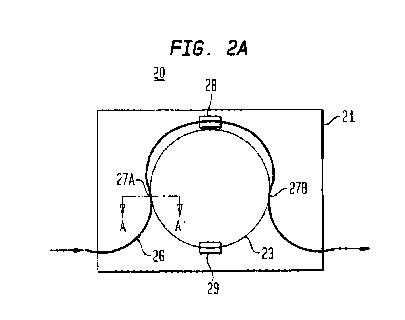
- Figs. 2A and 2B are top and cross sectional views, respectively, of a first embodiment of an all-pass filter 20 formed on a substrate 21.
- the filter 20 comprises a first layer 22 including a waveguiding optical ring resonator 23, a second layer 24 for spacing, and a third layer 25 including a waveguide 26 curving in substantial conformity to a portion of resonator 23.
- the waveguide 26 is optically coupled to the resonator 23 vertically through spacer layer 24 at the coupling regions 27A and 27B where the waveguide and resonator overlap.
- the waveguide 26 is curved so that the segment of waveguide 26 between the couplers 27A and 27B has substantially the same pathlength as the segment of the resonator between the couplers.
- the waveguide 26 and the resonator 23 are horizontally spaced apart (i.e. do not overlap) by a sufficient distance that they are optically isolated in these non-coupling regions.
- the cross section in Fig. 2A is taken across the line A - A', and shows the waveguide (core) 26 overlying the resonator (core) 23 across the spacing layer 24 in the coupling region 27A.
- the waveguide 26 is provided with a first phase-shifter 28 in the segment between 27A and 27B.
- the resonator 23 is provided with a second phase-shifter 29 in the region downstream of 27B.
- phase-shifters 28 and 29 can be local heaters. If so, the material of the layer 25 can have a large temperature dependence compared with the temperature dependence of layer 22.
- layer 22 can be silica and layer 25 can be a polymer. In this way, heat used to tune waveguide 26 will have minimal effect on resonator 23.
- the substrate 21 can be silicon
- the first (cladding) layer, 22 can be silica with the resonator (core) 23 formed of a higher index phosphous-doped (P-doped) or Ge-doped silica.
- the spacer layer can be silica having a thickness in the range 0 - 0.5 ⁇ m.
- the third (cladding) layer 25 can be polymer such as a mixture of halogenated acrylates having a refractive index with a large temperature dependence as compared with that of layer 22.
- the waveguide core 26 in layer 25 can be formed by locally changing the mixture of halogenated acrylates to increase the refractive index over the cladding layer.
- the resonator and waveguide horizontally coincide.
- they are spaced apart by a distance sufficient to prevent coupling (typically an edge-to-edge spacing of more than 5 ⁇ m).
- Figs. 3A and 3B are top and cross sectional views of a second embodiment of an all-pass filter similar to that of Fig. 2 except that spacer layer 24 is a thick layer capable of optically isolating the waveguide from the resonator except in the coupling regions 27A and 27B where the layer 24 is thinned to permit coupling.
- a resulting coupling region (27A) is shown in Fig. 3B, which is a cross section along the line B - B'. With this arrangement the waveguide 26 can overlap the resonator even in the non-coupling region between 27A and 27B.
Landscapes
- Physics & Mathematics (AREA)
- General Physics & Mathematics (AREA)
- Optics & Photonics (AREA)
- Nonlinear Science (AREA)
- Engineering & Computer Science (AREA)
- Microelectronics & Electronic Packaging (AREA)
- Optical Integrated Circuits (AREA)
- Optical Modulation, Optical Deflection, Nonlinear Optics, Optical Demodulation, Optical Logic Elements (AREA)
Abstract
Description
Claims (3)
- A tunable optical all-pass filter comprising:a substrate;a first layer on said substrate including a waveguide optical ring resonator;a second layer;a third layer including a curved waveguide;the curved waveguide optically coupled to the optical ring resonator through the second layer by at least two optical couplers;a first phase shifter for adjusting the optical pathlengths of the ring resonator; anda second phase shifter for adjusting the path length of the waveguide between the two optical couplers.
- The all-pass filter of claim 1 wherein the second layer is of uniform thickness and the curved waveguide is offset from the resonator in the regions outside the couplers to provide optical isolation between the waveguide and the resonator.
- The all-pass filter of claim 1 wherein the second layer in the regions outside the coupler is sufficiently thick to provide optical isolation between the waveguide and the resonator.
Priority Applications (1)
| Application Number | Priority Date | Filing Date | Title |
|---|---|---|---|
| EP08019245A EP2026123B1 (en) | 2000-05-17 | 2001-05-08 | Tunable all-pass optical filters with large free spectral ranges |
Applications Claiming Priority (2)
| Application Number | Priority Date | Filing Date | Title |
|---|---|---|---|
| US573086 | 1995-12-15 | ||
| US09/573,086 US6389203B1 (en) | 2000-05-17 | 2000-05-17 | Tunable all-pass optical filters with large free spectral ranges |
Related Child Applications (1)
| Application Number | Title | Priority Date | Filing Date |
|---|---|---|---|
| EP08019245A Division EP2026123B1 (en) | 2000-05-17 | 2001-05-08 | Tunable all-pass optical filters with large free spectral ranges |
Publications (2)
| Publication Number | Publication Date |
|---|---|
| EP1158326A2 true EP1158326A2 (en) | 2001-11-28 |
| EP1158326A3 EP1158326A3 (en) | 2004-02-04 |
Family
ID=24290587
Family Applications (2)
| Application Number | Title | Priority Date | Filing Date |
|---|---|---|---|
| EP08019245A Expired - Lifetime EP2026123B1 (en) | 2000-05-17 | 2001-05-08 | Tunable all-pass optical filters with large free spectral ranges |
| EP01304114A Ceased EP1158326A3 (en) | 2000-05-17 | 2001-05-08 | Tunable all-pass optical filters with large free spectral ranges |
Family Applications Before (1)
| Application Number | Title | Priority Date | Filing Date |
|---|---|---|---|
| EP08019245A Expired - Lifetime EP2026123B1 (en) | 2000-05-17 | 2001-05-08 | Tunable all-pass optical filters with large free spectral ranges |
Country Status (3)
| Country | Link |
|---|---|
| US (1) | US6389203B1 (en) |
| EP (2) | EP2026123B1 (en) |
| JP (1) | JP3877976B2 (en) |
Cited By (12)
| Publication number | Priority date | Publication date | Assignee | Title |
|---|---|---|---|---|
| DE10219244A1 (en) * | 2002-04-24 | 2003-11-13 | Fraunhofer Ges Forschung | Determining optical filter parameters involves defining ring resonator model segments, determining wavelength-dependent electrical energy, coupling factors, optimizing transmission function |
| EP1503229A1 (en) * | 2003-08-01 | 2005-02-02 | BAE SYSTEMS Information and Electronic Systems Integration, Inc. | Method of forming interlayer connections in integrated optical circuits, and devices formed using same |
| EP1372280A3 (en) * | 2002-05-17 | 2005-02-02 | Nec Corporation | Optical waveguide dispersion compensator and method of fabricating the same |
| WO2005036227A1 (en) * | 2003-09-16 | 2005-04-21 | Massachusetts Institute Of Technology | Ring resonator including nested mach zehnder module |
| CN100373193C (en) * | 2005-10-18 | 2008-03-05 | 电子科技大学 | S-shaped erbium-ytterbium co-doped phosphate high-gain optical waveguide, optical waveguide laser and optical waveguide amplifier |
| EP1959279A1 (en) * | 2007-02-14 | 2008-08-20 | NEC Corporation | Optical module with reduced thermal contraction stress |
| CN104062712A (en) * | 2014-07-17 | 2014-09-24 | 广东威创视讯科技股份有限公司 | Smoothing structure applied to LED and LED display screen |
| EP2781957A1 (en) * | 2013-03-21 | 2014-09-24 | Alcatel Lucent | Optical filtering device with resonator ring |
| WO2019015779A1 (en) * | 2017-07-21 | 2019-01-24 | Telefonaktiebolaget Lm Ericsson (Publ) | Chromatic dispersion compensation |
| CN110764284A (en) * | 2019-10-18 | 2020-02-07 | 中国地质大学(武汉) | Large-range bandwidth-adjustable microwave photon filter based on silicon-based micro-ring |
| CN113031162A (en) * | 2021-03-15 | 2021-06-25 | 中国科学院半导体研究所 | Optical filter |
| CN113474704A (en) * | 2019-02-14 | 2021-10-01 | 古河电气工业株式会社 | Ring resonator filter element |
Families Citing this family (27)
| Publication number | Priority date | Publication date | Assignee | Title |
|---|---|---|---|---|
| US6928091B1 (en) * | 2001-09-26 | 2005-08-09 | Oewaves, Inc. | Opto-electronic oscillator including a tunable electro-optic filter |
| JP2003131055A (en) * | 2001-10-25 | 2003-05-08 | Fujitsu Ltd | Optical waveguide and method of manufacturing the same |
| JP2003315752A (en) * | 2002-04-24 | 2003-11-06 | Fujitsu Ltd | Chromatic dispersion compensation filter |
| JP4079146B2 (en) * | 2002-09-20 | 2008-04-23 | 凸版印刷株式会社 | Manufacturing method of optical waveguide |
| JP3995686B2 (en) * | 2003-05-08 | 2007-10-24 | 富士通株式会社 | Dispersion slope compensator |
| US7657139B2 (en) * | 2004-06-07 | 2010-02-02 | The Regents Of The University Of California | Y-junction reflector tunable delay or resonator waveguide devices |
| US20060078258A1 (en) * | 2004-10-07 | 2006-04-13 | University Of Toledo | Apparatus and method for trimming and tuning coupled photonic waveguides |
| CA2499651A1 (en) * | 2005-03-04 | 2006-09-04 | Itf Technologies Optiques Inc./Itf Optical Technologies Inc. | All-fiber phase controlled delay interferometer and method of making the same |
| WO2008118465A2 (en) * | 2007-03-26 | 2008-10-02 | Massachusetts Institute Of Technology | Hitless tuning and switching of optical resonator amplitude and phase responses |
| US7805026B2 (en) * | 2007-10-09 | 2010-09-28 | Alcatel-Lucent Usa Inc. | Resonator-assisted control of radio-frequency response in an optical modulator |
| US8014676B2 (en) * | 2008-02-22 | 2011-09-06 | Alcatel Lucent | CMOS-compatible tunable microwave photonic band-stop filter |
| WO2010138849A1 (en) * | 2009-05-29 | 2010-12-02 | Massachusetts Institute Of Technology | Cavity dynamics compensation in resonant optical modulators |
| CN102680211B (en) * | 2012-05-28 | 2015-01-14 | 中国电子科技集团公司第四十一研究所 | Method for testing polarization coupling strength of polarization maintaining optical fiber based on polarization beam-splitting interference technique |
| US9831360B2 (en) | 2012-10-09 | 2017-11-28 | Mcmaster University | Integrated thermal stabilization of a microring resonator |
| EP3051367B1 (en) | 2015-01-28 | 2020-11-25 | Honeywell spol s.r.o. | An approach and system for handling constraints for measured disturbances with uncertain preview |
| EP3056706A1 (en) | 2015-02-16 | 2016-08-17 | Honeywell International Inc. | An approach for aftertreatment system modeling and model identification |
| EP3125052B1 (en) | 2015-07-31 | 2020-09-02 | Garrett Transportation I Inc. | Quadratic program solver for mpc using variable ordering |
| US10272779B2 (en) | 2015-08-05 | 2019-04-30 | Garrett Transportation I Inc. | System and approach for dynamic vehicle speed optimization |
| US10415492B2 (en) | 2016-01-29 | 2019-09-17 | Garrett Transportation I Inc. | Engine system with inferential sensor |
| US10124750B2 (en) | 2016-04-26 | 2018-11-13 | Honeywell International Inc. | Vehicle security module system |
| US10036338B2 (en) | 2016-04-26 | 2018-07-31 | Honeywell International Inc. | Condition-based powertrain control system |
| WO2018101918A1 (en) | 2016-11-29 | 2018-06-07 | Honeywell International Inc. | An inferential flow sensor |
| US20190049666A1 (en) * | 2017-08-12 | 2019-02-14 | Luxtera, Inc. | Method And Systems For All Optical Tunable Equalizers |
| US11057213B2 (en) | 2017-10-13 | 2021-07-06 | Garrett Transportation I, Inc. | Authentication system for electronic control unit on a bus |
| US10215925B1 (en) | 2018-08-22 | 2019-02-26 | Mcmaster University | Systems and methods for resonance stabilization of microring resonator |
| EP3935424A4 (en) | 2019-04-10 | 2022-05-04 | Ayar Labs, Inc. | SYSTEMS AND METHODS FOR COUPLING LIGHT IN A MULTIMODE RESONATOR |
| CN114812810B (en) * | 2022-05-18 | 2025-08-29 | 南京航空航天大学 | Spectral sampling element and computational spectral measurement device |
Family Cites Families (12)
| Publication number | Priority date | Publication date | Assignee | Title |
|---|---|---|---|---|
| JPS5434847A (en) * | 1977-08-23 | 1979-03-14 | Matsushita Electric Ind Co Ltd | Optical propagating device |
| JPS57604A (en) * | 1980-06-03 | 1982-01-05 | Nippon Telegr & Teleph Corp <Ntt> | Formation of three-dimensionally disposed glass waveguide |
| US4695121A (en) * | 1985-01-28 | 1987-09-22 | Polaroid Corporation | Integrated optic resonant structres and fabrication method |
| ATE71718T1 (en) * | 1987-06-04 | 1992-02-15 | Walter Lukosz | OPTICAL MODULATION AND MEASUREMENT PROCEDURE. |
| JP2567175B2 (en) * | 1992-02-24 | 1996-12-25 | 日本電信電話株式会社 | Waveguide type optical multiplexer / demultiplexer |
| JPH05323138A (en) * | 1992-05-18 | 1993-12-07 | Nippon Telegr & Teleph Corp <Ntt> | Stacked optical waveguide circuit |
| JPH06110091A (en) * | 1992-09-29 | 1994-04-22 | Nippon Telegr & Teleph Corp <Ntt> | Waveguide type optical coupling circuit |
| JP3196797B2 (en) * | 1993-07-12 | 2001-08-06 | 日本電信電話株式会社 | Manufacturing method of laminated quartz optical waveguide |
| JP3654383B2 (en) * | 1995-12-07 | 2005-06-02 | Kddi株式会社 | Optical add / drop multiplexer |
| JPH11160741A (en) * | 1997-09-26 | 1999-06-18 | Nippon Telegr & Teleph Corp <Ntt> | Stacked thermo-optic switch, switch matrix and optical add / drop multiplexer including the switch as a component |
| DE19849862C1 (en) * | 1998-10-29 | 2000-04-06 | Alcatel Sa | Thermo-optical switch has polymer light conductor with temperature control arrangement at coupling points with two optical glass conductors in parallel plane |
| US6289151B1 (en) * | 1998-10-30 | 2001-09-11 | Lucent Technologies Inc. | All-pass optical filters |
-
2000
- 2000-05-17 US US09/573,086 patent/US6389203B1/en not_active Expired - Lifetime
-
2001
- 2001-05-08 EP EP08019245A patent/EP2026123B1/en not_active Expired - Lifetime
- 2001-05-08 EP EP01304114A patent/EP1158326A3/en not_active Ceased
- 2001-05-17 JP JP2001147159A patent/JP3877976B2/en not_active Expired - Fee Related
Cited By (19)
| Publication number | Priority date | Publication date | Assignee | Title |
|---|---|---|---|---|
| DE10219244A1 (en) * | 2002-04-24 | 2003-11-13 | Fraunhofer Ges Forschung | Determining optical filter parameters involves defining ring resonator model segments, determining wavelength-dependent electrical energy, coupling factors, optimizing transmission function |
| EP1372280A3 (en) * | 2002-05-17 | 2005-02-02 | Nec Corporation | Optical waveguide dispersion compensator and method of fabricating the same |
| US6947642B2 (en) | 2002-05-17 | 2005-09-20 | Nec Corporation | Optical resonator waveguide device and method of fabricating the same |
| EP1503229A1 (en) * | 2003-08-01 | 2005-02-02 | BAE SYSTEMS Information and Electronic Systems Integration, Inc. | Method of forming interlayer connections in integrated optical circuits, and devices formed using same |
| WO2005036227A1 (en) * | 2003-09-16 | 2005-04-21 | Massachusetts Institute Of Technology | Ring resonator including nested mach zehnder module |
| CN100373193C (en) * | 2005-10-18 | 2008-03-05 | 电子科技大学 | S-shaped erbium-ytterbium co-doped phosphate high-gain optical waveguide, optical waveguide laser and optical waveguide amplifier |
| CN101299082B (en) * | 2007-02-14 | 2012-02-29 | 日本电气株式会社 | Optical module |
| US7684133B2 (en) | 2007-02-14 | 2010-03-23 | Nec Corporation | Optical module |
| EP1959279A1 (en) * | 2007-02-14 | 2008-08-20 | NEC Corporation | Optical module with reduced thermal contraction stress |
| EP2781957A1 (en) * | 2013-03-21 | 2014-09-24 | Alcatel Lucent | Optical filtering device with resonator ring |
| US9395596B2 (en) | 2013-03-21 | 2016-07-19 | Commissariat A L'energie Atomique Et Aux Energies Alternatives | Ring resonator comprising optical filtering device |
| CN104062712A (en) * | 2014-07-17 | 2014-09-24 | 广东威创视讯科技股份有限公司 | Smoothing structure applied to LED and LED display screen |
| WO2019015779A1 (en) * | 2017-07-21 | 2019-01-24 | Telefonaktiebolaget Lm Ericsson (Publ) | Chromatic dispersion compensation |
| US11243356B2 (en) | 2017-07-21 | 2022-02-08 | Telefonaktiebolaget Lm Ericsson (Publ) | Chromatic dispersion compensation |
| CN113474704A (en) * | 2019-02-14 | 2021-10-01 | 古河电气工业株式会社 | Ring resonator filter element |
| US12282188B2 (en) | 2019-02-14 | 2025-04-22 | Furukawa Electric Co., Ltd. | Ring-resonator filter device |
| CN110764284A (en) * | 2019-10-18 | 2020-02-07 | 中国地质大学(武汉) | Large-range bandwidth-adjustable microwave photon filter based on silicon-based micro-ring |
| CN113031162A (en) * | 2021-03-15 | 2021-06-25 | 中国科学院半导体研究所 | Optical filter |
| CN113031162B (en) * | 2021-03-15 | 2022-08-05 | 中国科学院半导体研究所 | Optical filter |
Also Published As
| Publication number | Publication date |
|---|---|
| EP1158326A3 (en) | 2004-02-04 |
| EP2026123A3 (en) | 2009-04-01 |
| JP3877976B2 (en) | 2007-02-07 |
| EP2026123A2 (en) | 2009-02-18 |
| US6389203B1 (en) | 2002-05-14 |
| JP2002022983A (en) | 2002-01-23 |
| EP2026123B1 (en) | 2011-07-06 |
Similar Documents
| Publication | Publication Date | Title |
|---|---|---|
| US6389203B1 (en) | Tunable all-pass optical filters with large free spectral ranges | |
| US6259847B1 (en) | Optical communication system including broadband all-pass filter for dispersion compensation | |
| US6961492B2 (en) | Tunable dispersion compensator | |
| US8781331B2 (en) | Controllable optical add/drop multiplexer | |
| US10142032B2 (en) | Temperature insensitive delay line interferometer | |
| JPH0799478A (en) | Dispersion compensating apparatus and method for fiber optic transmission system | |
| US20120002296A1 (en) | Optical Band Splitter/Combiner Device Comprising a Three-Arms Interferometer | |
| US7020398B2 (en) | Dispersion slope equalizer | |
| US20030202749A1 (en) | Integrated optical dual dispersion compensator for compensating both chromatic and polarization mode dispersion | |
| US11002913B2 (en) | Optical dispersion compensator on silicon | |
| US20060002653A1 (en) | Apparatus for an optical circuit having a flat wavelength response | |
| US6728446B2 (en) | Compact wavelength routing device having substantially flat passband | |
| US20070292079A1 (en) | Tunable optical dispersion compensators | |
| JPH0660982B2 (en) | Waveguide-type Matsuha-Tsender optical interferometer | |
| US10126629B1 (en) | Optical dispersion compensator on silicon | |
| US7116907B1 (en) | Acousto-optical tunable filters cascaded together | |
| EP1158318A2 (en) | Reconfigurable multi-channel filters having enhanced channel bandwidth | |
| US12451966B1 (en) | Optical communication systems and silicon photonics passive multiplexers and demultiplexers having Mach-Zehnder interferometer structures | |
| US6351586B1 (en) | Wavelength dependent phase delay device | |
| US7356219B2 (en) | Integrated optical add/drop device having switching function | |
| JPH0659291A (en) | Waveguide type optical multiplexer-branching filter for four-wave multiplex transmission and eight-wave multiple transmission | |
| JPH05323389A (en) | Optical variable branching filter device | |
| JP3128974B2 (en) | Waveguide type optical multiplexer / demultiplexer | |
| JPH0660803B2 (en) | Matsu Ha Tsuender-type optical interferometer | |
| Madsen et al. | An all-pass filter for tunable dispersion and dispersion slope compensation |
Legal Events
| Date | Code | Title | Description |
|---|---|---|---|
| PUAI | Public reference made under article 153(3) epc to a published international application that has entered the european phase |
Free format text: ORIGINAL CODE: 0009012 |
|
| AK | Designated contracting states |
Kind code of ref document: A2 Designated state(s): AT BE CH CY DE DK ES FI FR GB GR IE IT LI LU MC NL PT SE TR |
|
| AX | Request for extension of the european patent |
Free format text: AL;LT;LV;MK;RO;SI |
|
| PUAL | Search report despatched |
Free format text: ORIGINAL CODE: 0009013 |
|
| AK | Designated contracting states |
Kind code of ref document: A3 Designated state(s): AT BE CH CY DE DK ES FI FR GB GR IE IT LI LU MC NL PT SE TR |
|
| AX | Request for extension of the european patent |
Extension state: AL LT LV MK RO SI |
|
| RIC1 | Information provided on ipc code assigned before grant |
Ipc: 7G 02B 6/293 B Ipc: 7G 02F 1/225 B Ipc: 7G 02F 1/313 A |
|
| 17P | Request for examination filed |
Effective date: 20040724 |
|
| AKX | Designation fees paid |
Designated state(s): DE FR GB |
|
| 17Q | First examination report despatched |
Effective date: 20041111 |
|
| APBK | Appeal reference recorded |
Free format text: ORIGINAL CODE: EPIDOSNREFNE |
|
| APBN | Date of receipt of notice of appeal recorded |
Free format text: ORIGINAL CODE: EPIDOSNNOA2E |
|
| APAZ | Date of receipt of statement of grounds of appeal deleted |
Free format text: ORIGINAL CODE: EPIDOSDNOA3E |
|
| APBR | Date of receipt of statement of grounds of appeal recorded |
Free format text: ORIGINAL CODE: EPIDOSNNOA3E |
|
| APAF | Appeal reference modified |
Free format text: ORIGINAL CODE: EPIDOSCREFNE |
|
| RAP3 | Party data changed (applicant data changed or rights of an application transferred) |
Owner name: LUCENT TECHNOLOGIES INC. |
|
| APBT | Appeal procedure closed |
Free format text: ORIGINAL CODE: EPIDOSNNOA9E |
|
| STAA | Information on the status of an ep patent application or granted ep patent |
Free format text: STATUS: THE APPLICATION HAS BEEN REFUSED |
|
| 18R | Application refused |
Effective date: 20081127 |
|
| R18R | Application refused (corrected) |
Effective date: 20110927 |