EP1158302A2 - Method and apparatus for probing a conductor of an array of closely-spaced conductors - Google Patents
Method and apparatus for probing a conductor of an array of closely-spaced conductors Download PDFInfo
- Publication number
- EP1158302A2 EP1158302A2 EP01304043A EP01304043A EP1158302A2 EP 1158302 A2 EP1158302 A2 EP 1158302A2 EP 01304043 A EP01304043 A EP 01304043A EP 01304043 A EP01304043 A EP 01304043A EP 1158302 A2 EP1158302 A2 EP 1158302A2
- Authority
- EP
- European Patent Office
- Prior art keywords
- resistor
- input
- signal
- amplifier
- reference level
- Prior art date
- Legal status (The legal status is an assumption and is not a legal conclusion. Google has not performed a legal analysis and makes no representation as to the accuracy of the status listed.)
- Granted
Links
Images


Classifications
-
- G—PHYSICS
- G01—MEASURING; TESTING
- G01R—MEASURING ELECTRIC VARIABLES; MEASURING MAGNETIC VARIABLES
- G01R1/00—Details of instruments or arrangements of the types included in groups G01R5/00 - G01R13/00 and G01R31/00
- G01R1/02—General constructional details
- G01R1/06—Measuring leads; Measuring probes
- G01R1/067—Measuring probes
- G01R1/06766—Input circuits therefor
Definitions
- the subject invention generally concerns the field of probing a device under test, and specifically concerns probing a connection point of a ball grid array (BGA) circuit, or a conductor of a closely-spaced array of conductors (i.e., signal lines).
- BGA ball grid array
- a ball grid array (BGA) device is an integrated circuit having multiple contact points typically arranged in a 50-mil ball-spacing grid formation beneath the body of the integrated circuit.
- BGA ball grid array
- a method and apparatus for probing a terminal of a ball grid array device, or a conductor of an array of closely-spaced conductors preferably employs a buried tip resistor located substantially adjacent to the point to be monitored. In this way, a relatively short stub is provided from the connection point to the tip resistor.
- a receiver amplifier arrangement substantially eliminates an offset error that is exhibited in prior art amplifier arrangements, the offset error being introduced into the signal to be measured due to variation in the resistance value of tip resistor.
- buried resistors are not an essential element of the subject invention, but rather, the subject invention is applicable in probing situations involving the use of tip resistors having a tolerance range greater than 1%.
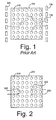
- FIGURE 1 shows a ball grid array device and tip resistor array in accordance with the prior art.
- FIGURE 2 shows a ball grid array device and buried tip resistors in accordance with the subject invention.
- FIGURE 3 shows a receiver amplifier arrangement in accordance with the prior art.
- FIGURE 4 is an illustration of waveforms exhibiting an offset error due to resistance value variation in the tip resistor (R TIP ) of FIGURE 2.
- FIGURE 5 shows a receiver amplifier arrangement in accordance with the subject invention.
- FIGURE 6 is an illustration of waveforms exhibiting substantially no offset error despite resistance value variation in the isolation resistors of FIGURE 2.
- FIGURE 7 shows a simplified circuit model useful for understanding the invention.
- the subject invention allows sampling (i.e., acquiring) of high-speed tight-tolerance digital signals from a microprocessor bus, or the like, while keeping the probing end as small as possible by using buried-resistor technology, despite the poor tolerance typically exhibited by buried resistors.
- a ball grid array (BGA) device 100 has an array of connection points 110 arranged beneath the device in a grid formation (i.e., typically 50 mils on center, although other ball-grid spacings are used). The connection points are shown as dotted circles to indicate that they are disposed beneath BGA device 100.
- Arrays of tip (or isolation) resistors 120 are disposed as close as possible along the periphery of the ball grid device. Connection between one of connection points 110 of the ball grid array 100 and the input end of a particular tip resistor of resistor array 120 is accomplished by means of conductive printed circuit traces 130.
- the tip resistors of resistor array 120 typically have a tolerance of no greater than 1%.
- traces 130 may be considered to be the tip of a probe coupled to a connection point 110.
- these traces 130 or paths also known as stubs
- these traces 130 or paths must follow relatively long and circuitous routes to make these connections. For example, if a BGA device is square and measures 2 inches (approximately 5 cm) on a side, then the shortest path to the input end of the closest tip (i.e., isolation) resistor is 1 inch (2.54 cm) long.
- These long and often circuitous routes i.e., long stub lengths
- cause the signals being conveyed along these routes to exhibit undesirable ringing, overshoot, or to exhibit a plateau close to a test reference voltage.
- the term "tip resistor”, as used herein, means the input resistor of a probe-like arrangement comprising a printed conductive trace, resistors, a transmission line, and an amplifier.
- the tip resistor As close as possible to the BGA connection point to be monitored. It is further herein recognized that the desirable tip resistor placement can be realized through the use of buried resistor technology. That is, the resistors are made small enough to fit within a BGA pad array, and are buried within the layers of the FR4 circuit board material.
- a BGA device 200 has an array of connection points (terminals) 210 arranged beneath the device in a grid formation (i.e., typically 50 mils on center). Tip (isolation) resistors 220 are disposed as close as possible to the desired connection points of the ball grid device. Connection between one of connection points 210 of the ball grid array 200 and the input end of a resistor 220 is accomplished by means of relatively short (e.g., 0.01 inch (254 ⁇ m)) conductive printed circuit traces 225. The remaining portion of the path 230 out from beneath the BGA device is isolated by a tip resistor 220, and does not substantially contribute the undesirable effects noted above.
- relatively short e.g. 0.01 inch (254 ⁇ m)
- buried resistors solved the routing problem with its associated ringing and overshoot problems, but unfortunately, caused another problem of its own.
- buried resistors are made small enough to fit within a 50-mil or smaller ball grid array, or within other arrays of closely-spaced conductors, their resistive tolerance degrades to over +/- 20%.
- the actual resistance value for a nominal 200-ohm resistor may in fact vary from 160 ohms to 240 ohms. This variation in resistor value causes problems when the buried resistor is used as the "tip" resistor in a traditional passive probing arrangement. It is also herein recognized that the same problem arises when attempting to probe a conductor of an array of closely-spaced conductors.
- closely-spaced conductors means an array of conductors or connection points having a lower limit of a center to center spacing larger than the width of the buried resistor and no greater than 0.2 inches. Over 0.2 inches, surface mount low tolerance solutions exist.
- FIGURE 3 shows a simplified version of such a typical receiver amplifier as known from the prior art.
- resistor R TIP represents a tip (i.e., isolation) resistor 220 of FIGURE 2 of the subject invention (assuming that the arrangement of FIGURE 2 is used in conjunction with prior art circuit FIGURE 3).
- the signal applied to a probe tip is conveyed through resistor R TIP and transmission line 310 to the plus input of amplifier 320.
- Transmission Line 310 is said to exhibit an impedance of Z O .
- the plus input of amplifier 320 is biased by a voltage supply V TERM applied to a node V X through a termination resistor R TERM which has a resistance approximately equal to Z O .
- the minus input of amplifier 320 is bias to a threshold voltage by a voltage source V THRESHOLD .
- amplifier 320 operates as a comparator, producing an output when its input threshold level is traversed. That is, when the signal developed at node V X exhibits a greater amplitude than the signal applied to the minus input, then amplifier 320 produces a high level output signal. Conversely, when the signal developed at node V X exhibits an equal or lower amplitude than the signal applied to the minus input, then amplifier 320 produces a low level output signal.
- Resistor R TIP limits the probing network load as seen by the probed point.
- Resistor R TERM represents the termination circuit that matches the impedance of Transmission Line 310 to substantially eliminate reflections from the receiver circuit back into the circuit under test.
- Source V TERM presents a low impedance return path to the transmission line signal, with a possible non-zero offset in potential.
- Source V THRESHOLD sets a threshold that is determined to be the center of the expected signal swing, as seen at node V X . That set point will generally correspond to the original signal reference voltage at the probed point (i.e., 1.0 volts for GTL+).
- FIGURE 3 is not suitable for use with the buried tip resistor arrangement of FIGURE 2 because of the above-noted resistance variation of resistor R TIP .
- resistor R TIP and resistor R TERM form a voltage divider, and variation in the value of resistor R TIP adversely affects the voltage divider ratio. This is important because, when R TIP exhibits poor resistive tolerance (i.e., is subject to resistive variation of greater than 1% channel to channel from the nominal value), then edge measurement (i.e., edge placement) accuracy will be poor. This condition is caused by a DC offset developed at summing node V X . This is the result of setting source Vterm to 0 volts (or any other voltage level than the original signal reference voltage).
- the resistance variation in R TIP causes signal variation at node V X , and in order to compensate for the signal variation at node V X , the threshold level V THRESHOLD must be made to vary accordingly.
- V THRESHOLD Changing the value of V THRESHOLD for each channel is not a practical solution for many applications, because each channel would have to be calibrated based upon the particular value for each individual R TIP .
- the maximum amount of variation in resistor R TIP that can be tolerated depends upon the particular application. Factors that affect this decision are the amount of signal swing, receiver amplifier sensitivity, edge-placement requirements, and ambient noise. For example, when monitoring a GTL+ signal, a comparator having 100mv differential sensitivity was found to operate in an acceptable fashion even when resistor R TIP had a tolerance of+/- 30%.
- FIGURE 4 is an illustration of waveform diagrams showing the adverse effects of variation in the resistance value of R TIP , when source V TERM is set and held to zero volts.
- waveform 400 is the waveform observed at the probe point
- waveforms 410 and 420 are waveforms developed at node V X .
- Waveform 420 is the expected waveform when resistor R TIP exhibits its nominal value.
- Waveform 410 has a greater amplitude and offset than does waveform 420, and results from resistor R TIP exhibiting a resistance value less than nominal.
- the threshold crossing point on waveform 420 is delayed in time by an amount ⁇ t due to its undesirable offset. That is, receiver amplifier 320 will see the input voltage developed at node V X (as represented by waveforms 410 and 420) traverse through the threshold region 430 at different times (i.e., at different points on the waveform).
- the amplifier arrangement of FIGURE 5 has been found to be substantially immune to such resistor R TIP variations, and to significantly reduce the above-noted offset error and corresponding timing error.
- the second difference is that the negative (i.e., minus or inverting) input terminal of amplifier 520 is coupled to V REFERENCE .
- the third, and most important, difference is that V REFERENCE must be set to the same potential as the center of the swing at the probe point (i.e., 1.0 volts for GTL+).
- FIGURE 5 functions independently with respect to variations in the resistance of resistor R TIP . This is true because V REFERENCE (the center of the expected signal swing) is used to terminate the signal seen at node V X . As a result, as the resistance value of resistor R TIP varies, the amplitude of the signal at V X changes, but the signal swing remains centered about V REFERENCE because the DC component has been removed.
- V REFERENCE the center of the expected signal swing
- the subject invention is also applicable to the field of Logic Analyzers. It is envisioned that the subject invention could be implemented on an acquisition ASIC (Application Specific Integrated Circuit) for a logic analyzer application. In such a logic analyzer application, a similar topology to that of FIGURE 5 should be used, a programmable V TERM source would be required.
- acquisition ASIC Application Specific Integrated Circuit
- Equation (2) represents the typical prior art passive probing topology of FIGURE 3 in which V TERM does not equal V REFERENCE .
- the first term in equation (2) is an attenuated signal term swinging about zero volts.
- the remaining two terms are DC offset components that will vary in amplitude with variations in resistance value of R TIP as shown in FIGURE 4.
- Equation (4) has been reduced to two components; the attenuated AC signal and a fixed DC offset of V REFERENCE . As is clearly shown in FIGURE 4, there is no effect of R TIP resistance variation in the DC offset.
- V X (V SIG + V REF ) * R TERM R TIP +R TERM + (V TERM ) * R TIP R TIP + R TERM Expanding: Eq.
- the subject invention was described with respect to buried resistors, it should be noted that it is also useful with any form of loose tolerance resistors (i.e., resistors with a tolerance greater than substantially 1%). It is envisioned that the circuitry described above can be used in conjunction with an oscilloscope, a logic analyzer, or other instrument for monitoring signals from a device under test. However, the subject invention is not limited to test and measurement instruments, but may also be used for coupling signals between BGA devices and other circuitry on a printed circuit card. While the invention was described with respect to BGA devices, it should be noted that the invention is also useful for probing a conductor of a plurality of closely-conductors (such as a bus), or array of closely spaced conductors. All of the above modifications are therefore deemed to lie within the scope of the following claims.
Landscapes
- Physics & Mathematics (AREA)
- General Physics & Mathematics (AREA)
- Tests Of Electronic Circuits (AREA)
- Testing Of Individual Semiconductor Devices (AREA)
- Wire Bonding (AREA)
- Amplifiers (AREA)
- Semiconductor Integrated Circuits (AREA)
- Testing Of Short-Circuits, Discontinuities, Leakage, Or Incorrect Line Connections (AREA)
Abstract
Description
Solving for Vx:
However, the subject invention is not limited to test and measurement instruments, but may also be used for coupling signals between BGA devices and other circuitry on a printed circuit card. While the invention was described with respect to BGA devices, it should be noted that the invention is also useful for probing a conductor of a plurality of closely-conductors (such as a bus), or array of closely spaced conductors. All of the above modifications are therefore deemed to lie within the scope of the following claims.
Claims (10)
- An arrangement for probing a signal at a terminal of an electronic device, comprising:an input coupled to said terminal for receiving said signal;a tip resistor having a tolerance in a range greater than 1%, said tip resistor having a first end coupled to said input for receiving said signal, and being physically located substantially adjacent to said terminal of said electronic device;a transmission line having an input end coupled to a second end of said tip resistor for receiving said signal, and having an output end; andan amplifier having a first input coupled to said output end of said transmission line for receiving said signal and amplifying said signal when said signal exceeds a predetermined reference value;said amplifier being biased to said reference level, said reference level being substantially identical to a reference level exhibited by said signal at said input.
- The arrangement of claim 1, wherein said amplifier is biased to said reference level by a biasing circuit comprising:a source of reference level potential; anda second resistor having a first end coupled to said source of reference level potential at a junction, and having a second end coupled to said output end of said transmission line, said transmission line having a characteristic impedance and said second resistor having a value substantially equal to said characteristic impedance.
- The arrangement of claim 2, wherein said junction of said source of reference level potential and said second resistor is coupled to a second input of said amplifier.
- The arrangement of claim 3, wherein said tip resistor is an isolation resistor, first input of said amplifier is a non-inverting terminal, and said second input of said amplifier is an inverting terminal.
- An arrangement for probing a signal developed at a terminal of a ball grid array device mounted on a circuit board, said arrangement comprising:an electrical connection pad formed on said circuit board for connecting to said terminal of said ball grid array device for receiving said signal;an input coupled to said electrical connection pad for receiving said signal;an isolation resistor disposed within said circuit board, and being physically located substantially adjacent to said electrical connection pad, said isolation resistor having a first end coupled to said input, and having a second end;a transmission line having an input end coupled to said second end of said isolation resistor, andan amplifier coupled to said second end of said transmission line for amplifying signals above a predetermined threshold value;said amplifier being biased to a reference level substantially identical to a reference level exhibited by said signal at said input.
- The arrangement of claim 5, wherein said amplifier is biased to said reference level by a biasing circuit comprising:a source of reference level potential; anda second resistor having a first end coupled to said source of reference level potential at a junction, and having a second end coupled to said output end of said transmission line, said transmission line having a characteristic impedance and said second resistor having a value substantially equal to said characteristic impedance.
- The arrangement of claim 6, wherein said junction of said source of reference level potential and said second resistor is coupled to a second input of said amplifier.
- The arrangement of claim 7, wherein said first input of said amplifier is a non-inverting terminal, and said second input of said amplifier is an inverting terminal.
- A method for probing a signal developed at a conductor of an array of closely-spaced conductors formed on a circuit board, said method comprising the steps of:coupling an input stub to said conductor for receiving said signal;placing a tip resistor within said circuit board, said tip resistor being physically located substantially adjacent to said conductor, said tip resistor having a first end coupled to said conductor, and having a second end;coupling an input end of a transmission line to said second end of said tip resistor,coupling an amplifier to said second end of said transmission line for amplifying signals above a predetermined threshold value; andbiasing said amplifier to a reference level substantially identical to a reference level exhibited by said signal at said one conductor.
- The method of claim 9, wherein the biasing step further including the steps of:providing a source of reference level potential;providing a second resistor having a characteristic impedance substantially identical to a characteristic impedance of said transmission line;coupling a first end of said second resistor to said source of reference level potential at a junction;coupling a second a second end of said second resistor to said output end of said transmission line; andcoupling said junction to a second input of said amplifier.
Applications Claiming Priority (2)
| Application Number | Priority Date | Filing Date | Title |
|---|---|---|---|
| US577239 | 2000-05-23 | ||
| US09/577,239 US6462528B1 (en) | 2000-05-23 | 2000-05-23 | Method and apparatus for probing a conductor of an array of closely-spaced conductors |
Publications (3)
| Publication Number | Publication Date |
|---|---|
| EP1158302A2 true EP1158302A2 (en) | 2001-11-28 |
| EP1158302A3 EP1158302A3 (en) | 2003-10-22 |
| EP1158302B1 EP1158302B1 (en) | 2005-11-30 |
Family
ID=24307867
Family Applications (1)
| Application Number | Title | Priority Date | Filing Date |
|---|---|---|---|
| EP01304043A Expired - Lifetime EP1158302B1 (en) | 2000-05-23 | 2001-05-03 | Method and apparatus for probing a conductor of an array of closely-spaced conductors |
Country Status (5)
| Country | Link |
|---|---|
| US (1) | US6462528B1 (en) |
| EP (1) | EP1158302B1 (en) |
| JP (1) | JP4467833B2 (en) |
| CN (1) | CN1185499C (en) |
| DE (1) | DE60115322T2 (en) |
Cited By (1)
| Publication number | Priority date | Publication date | Assignee | Title |
|---|---|---|---|---|
| US12007420B2 (en) | 2019-03-19 | 2024-06-11 | Sony Semiconductor Solutions Corporation | Potential measurement device |
Families Citing this family (5)
| Publication number | Priority date | Publication date | Assignee | Title |
|---|---|---|---|---|
| US6806697B2 (en) * | 2002-04-05 | 2004-10-19 | Agilent Technologies, Inc. | Apparatus and method for canceling DC errors and noise generated by ground shield current in a probe |
| US20050086037A1 (en) * | 2003-09-29 | 2005-04-21 | Pauley Robert S. | Memory device load simulator |
| US6987397B2 (en) * | 2003-10-09 | 2006-01-17 | International Business Machines Corporation | Method and probe structure for implementing a single probe location for multiple signals |
| DE10355296B3 (en) * | 2003-11-27 | 2005-06-09 | Infineon Technologies Ag | Testing device for wafer testing of digital semiconductor circuits with signal amplifiers inserted in test signal channels for eliminating signal attentuation and noise |
| US20060061348A1 (en) * | 2004-09-20 | 2006-03-23 | Cannon James E | High frequency oscilloscope probe with unitized probe tips |
Family Cites Families (8)
| Publication number | Priority date | Publication date | Assignee | Title |
|---|---|---|---|---|
| US4403183A (en) * | 1981-04-10 | 1983-09-06 | Tektronix, Inc. | Active voltage probe |
| JPH01317077A (en) * | 1988-06-17 | 1989-12-21 | Toshiba Corp | Clamp circuit |
| JPH05122029A (en) * | 1991-10-30 | 1993-05-18 | Nec Corp | Digital clock generator |
| JPH06140484A (en) * | 1992-10-28 | 1994-05-20 | Nippon Telegr & Teleph Corp <Ntt> | Probe card |
| JPH10322139A (en) * | 1997-05-19 | 1998-12-04 | Oki Electric Ind Co Ltd | Input circuit |
| US6094045A (en) * | 1997-09-18 | 2000-07-25 | Fluke Corporation | Input ranging circuit for an electronic instrument |
| US6144213A (en) * | 1998-05-05 | 2000-11-07 | Agilent Technologies | Ball grid array probing technique |
| US6225816B1 (en) | 1999-04-08 | 2001-05-01 | Agilent Technologies, Inc. | Split resistor probe and method |
-
2000
- 2000-05-23 US US09/577,239 patent/US6462528B1/en not_active Expired - Fee Related
-
2001
- 2001-05-03 EP EP01304043A patent/EP1158302B1/en not_active Expired - Lifetime
- 2001-05-03 DE DE60115322T patent/DE60115322T2/en not_active Expired - Lifetime
- 2001-05-21 JP JP2001151610A patent/JP4467833B2/en not_active Expired - Fee Related
- 2001-05-23 CN CNB011169982A patent/CN1185499C/en not_active Expired - Fee Related
Cited By (1)
| Publication number | Priority date | Publication date | Assignee | Title |
|---|---|---|---|---|
| US12007420B2 (en) | 2019-03-19 | 2024-06-11 | Sony Semiconductor Solutions Corporation | Potential measurement device |
Also Published As
| Publication number | Publication date |
|---|---|
| JP4467833B2 (en) | 2010-05-26 |
| DE60115322T2 (en) | 2006-08-17 |
| US6462528B1 (en) | 2002-10-08 |
| EP1158302A3 (en) | 2003-10-22 |
| JP2002055144A (en) | 2002-02-20 |
| CN1185499C (en) | 2005-01-19 |
| EP1158302B1 (en) | 2005-11-30 |
| DE60115322D1 (en) | 2006-01-05 |
| CN1335511A (en) | 2002-02-13 |
Similar Documents
| Publication | Publication Date | Title |
|---|---|---|
| CA1271848A (en) | Wafer probe | |
| US6768328B2 (en) | Single point probe structure and method | |
| US7019544B1 (en) | Transmission line input structure test probe | |
| US6864694B2 (en) | Voltage probe | |
| US6806724B2 (en) | Probe for combined signals | |
| JP4866995B2 (en) | Probing method and apparatus | |
| US20010024116A1 (en) | Electronic probe for measuring high impedance tri-state logic circuits | |
| US20010002794A1 (en) | Split resistor probe and method | |
| JPS6195259A (en) | Improved wide-band contactor assembly for testing integratedcircuit device | |
| JP4689125B2 (en) | Improved test and calibration circuit and method in automatic test equipment | |
| US9261535B2 (en) | Active probe adaptor | |
| EP1158302B1 (en) | Method and apparatus for probing a conductor of an array of closely-spaced conductors | |
| EP3546975B1 (en) | Test arrangement and test method for characterizing a differential probe | |
| US7777509B2 (en) | Method and apparatus for electrical testing | |
| JPH11258274A (en) | Probe chip and cable loss compensation method | |
| US5880540A (en) | Switching apparatus with current limiting circuit | |
| US7042232B1 (en) | Cable and substrate compensating custom resistor | |
| US20060181293A1 (en) | Low impedance test fixture for impedance measurements | |
| US7078924B2 (en) | Methodology to accurately test clock to signal valid and slew rates of PCI signals | |
| US7342466B2 (en) | Hybrid coupler having resistive coupling and electromagnetic coupling | |
| JPH05218780A (en) | Probe attenuator | |
| US20240087776A1 (en) | Current shunt with canceling mutual inductance | |
| CN117686758A (en) | Shunt to cancel mutual inductance | |
| CN111721977A (en) | Surface mountable equipment that couples test and measurement instruments to the device under test | |
| Schwertner et al. | Obtaining more accurate resistance measurements using the six‐wire ohms measurement technique |
Legal Events
| Date | Code | Title | Description |
|---|---|---|---|
| PUAI | Public reference made under article 153(3) epc to a published international application that has entered the european phase |
Free format text: ORIGINAL CODE: 0009012 |
|
| AK | Designated contracting states |
Kind code of ref document: A2 Designated state(s): AT BE CH CY DE DK ES FI FR GB GR IE IT LI LU MC NL PT SE TR |
|
| AX | Request for extension of the european patent |
Free format text: AL;LT;LV;MK;RO;SI |
|
| PUAL | Search report despatched |
Free format text: ORIGINAL CODE: 0009013 |
|
| AK | Designated contracting states |
Kind code of ref document: A3 Designated state(s): AT BE CH CY DE DK ES FI FR GB GR IE IT LI LU MC NL PT SE TR |
|
| AX | Request for extension of the european patent |
Extension state: AL LT LV MK RO SI |
|
| RIC1 | Information provided on ipc code assigned before grant |
Ipc: 7G 01R 19/25 B Ipc: 7G 01R 1/067 A |
|
| 17P | Request for examination filed |
Effective date: 20040219 |
|
| 17Q | First examination report despatched |
Effective date: 20040325 |
|
| AKX | Designation fees paid |
Designated state(s): DE FR GB IT |
|
| GRAP | Despatch of communication of intention to grant a patent |
Free format text: ORIGINAL CODE: EPIDOSNIGR1 |
|
| GRAS | Grant fee paid |
Free format text: ORIGINAL CODE: EPIDOSNIGR3 |
|
| GRAA | (expected) grant |
Free format text: ORIGINAL CODE: 0009210 |
|
| AK | Designated contracting states |
Kind code of ref document: B1 Designated state(s): DE FR GB IT |
|
| REG | Reference to a national code |
Ref country code: GB Ref legal event code: FG4D |
|
| REF | Corresponds to: |
Ref document number: 60115322 Country of ref document: DE Date of ref document: 20060105 Kind code of ref document: P |
|
| ET | Fr: translation filed | ||
| PLBE | No opposition filed within time limit |
Free format text: ORIGINAL CODE: 0009261 |
|
| STAA | Information on the status of an ep patent application or granted ep patent |
Free format text: STATUS: NO OPPOSITION FILED WITHIN TIME LIMIT |
|
| 26N | No opposition filed |
Effective date: 20060831 |
|
| PGFP | Annual fee paid to national office [announced via postgrant information from national office to epo] |
Ref country code: GB Payment date: 20140527 Year of fee payment: 14 |
|
| PGFP | Annual fee paid to national office [announced via postgrant information from national office to epo] |
Ref country code: IT Payment date: 20140523 Year of fee payment: 14 Ref country code: DE Payment date: 20140529 Year of fee payment: 14 Ref country code: FR Payment date: 20140519 Year of fee payment: 14 |
|
| REG | Reference to a national code |
Ref country code: DE Ref legal event code: R119 Ref document number: 60115322 Country of ref document: DE |
|
| GBPC | Gb: european patent ceased through non-payment of renewal fee |
Effective date: 20150503 |
|
| PG25 | Lapsed in a contracting state [announced via postgrant information from national office to epo] |
Ref country code: IT Free format text: LAPSE BECAUSE OF NON-PAYMENT OF DUE FEES Effective date: 20150503 |
|
| REG | Reference to a national code |
Ref country code: FR Ref legal event code: ST Effective date: 20160129 |
|
| PG25 | Lapsed in a contracting state [announced via postgrant information from national office to epo] |
Ref country code: GB Free format text: LAPSE BECAUSE OF NON-PAYMENT OF DUE FEES Effective date: 20150503 Ref country code: DE Free format text: LAPSE BECAUSE OF NON-PAYMENT OF DUE FEES Effective date: 20151201 |
|
| PG25 | Lapsed in a contracting state [announced via postgrant information from national office to epo] |
Ref country code: FR Free format text: LAPSE BECAUSE OF NON-PAYMENT OF DUE FEES Effective date: 20150601 |