EP1155434B1 - Crossed-field amplifier with multipactor suppression - Google Patents
Crossed-field amplifier with multipactor suppression Download PDFInfo
- Publication number
- EP1155434B1 EP1155434B1 EP99961949A EP99961949A EP1155434B1 EP 1155434 B1 EP1155434 B1 EP 1155434B1 EP 99961949 A EP99961949 A EP 99961949A EP 99961949 A EP99961949 A EP 99961949A EP 1155434 B1 EP1155434 B1 EP 1155434B1
- Authority
- EP
- European Patent Office
- Prior art keywords
- crossed
- window
- cathode
- field device
- anode
- Prior art date
- Legal status (The legal status is an assumption and is not a legal conclusion. Google has not performed a legal analysis and makes no representation as to the accuracy of the status listed.)
- Expired - Lifetime
Links
- 230000001629 suppression Effects 0.000 title claims description 4
- 230000003993 interaction Effects 0.000 claims description 14
- 239000000463 material Substances 0.000 claims description 13
- 239000011248 coating agent Substances 0.000 claims description 11
- 238000000576 coating method Methods 0.000 claims description 11
- ZOKXTWBITQBERF-UHFFFAOYSA-N Molybdenum Chemical compound [Mo] ZOKXTWBITQBERF-UHFFFAOYSA-N 0.000 claims description 10
- 229910052750 molybdenum Inorganic materials 0.000 claims description 10
- 239000011733 molybdenum Substances 0.000 claims description 10
- 229910000476 molybdenum oxide Inorganic materials 0.000 claims description 8
- PQQKPALAQIIWST-UHFFFAOYSA-N oxomolybdenum Chemical compound [Mo]=O PQQKPALAQIIWST-UHFFFAOYSA-N 0.000 claims description 8
- 230000005684 electric field Effects 0.000 claims description 7
- 230000003321 amplification Effects 0.000 claims description 4
- 238000003199 nucleic acid amplification method Methods 0.000 claims description 4
- 230000002708 enhancing effect Effects 0.000 claims 1
- 230000037361 pathway Effects 0.000 claims 1
- 230000000694 effects Effects 0.000 description 12
- 238000010276 construction Methods 0.000 description 8
- 239000000919 ceramic Substances 0.000 description 6
- LTPBRCUWZOMYOC-UHFFFAOYSA-N beryllium oxide Inorganic materials O=[Be] LTPBRCUWZOMYOC-UHFFFAOYSA-N 0.000 description 4
- 238000004544 sputter deposition Methods 0.000 description 4
- RYGMFSIKBFXOCR-UHFFFAOYSA-N Copper Chemical compound [Cu] RYGMFSIKBFXOCR-UHFFFAOYSA-N 0.000 description 3
- 229910052802 copper Inorganic materials 0.000 description 3
- 239000010949 copper Substances 0.000 description 3
- 238000000151 deposition Methods 0.000 description 3
- 230000008021 deposition Effects 0.000 description 3
- 238000012986 modification Methods 0.000 description 3
- 230000004048 modification Effects 0.000 description 3
- 230000002093 peripheral effect Effects 0.000 description 3
- FRWYFWZENXDZMU-UHFFFAOYSA-N 2-iodoquinoline Chemical group C1=CC=CC2=NC(I)=CC=C21 FRWYFWZENXDZMU-UHFFFAOYSA-N 0.000 description 2
- QVGXLLKOCUKJST-UHFFFAOYSA-N atomic oxygen Chemical compound [O] QVGXLLKOCUKJST-UHFFFAOYSA-N 0.000 description 2
- 229910052790 beryllium Inorganic materials 0.000 description 2
- ATBAMAFKBVZNFJ-UHFFFAOYSA-N beryllium atom Chemical compound [Be] ATBAMAFKBVZNFJ-UHFFFAOYSA-N 0.000 description 2
- 230000002349 favourable effect Effects 0.000 description 2
- 239000007789 gas Substances 0.000 description 2
- 230000007246 mechanism Effects 0.000 description 2
- 229910052751 metal Inorganic materials 0.000 description 2
- 239000002184 metal Substances 0.000 description 2
- 238000000034 method Methods 0.000 description 2
- 230000003647 oxidation Effects 0.000 description 2
- 238000007254 oxidation reaction Methods 0.000 description 2
- 239000001301 oxygen Substances 0.000 description 2
- 229910052760 oxygen Inorganic materials 0.000 description 2
- BASFCYQUMIYNBI-UHFFFAOYSA-N platinum Chemical compound [Pt] BASFCYQUMIYNBI-UHFFFAOYSA-N 0.000 description 2
- 230000009467 reduction Effects 0.000 description 2
- 230000009466 transformation Effects 0.000 description 2
- 230000032683 aging Effects 0.000 description 1
- 238000004458 analytical method Methods 0.000 description 1
- 238000013459 approach Methods 0.000 description 1
- 230000005540 biological transmission Effects 0.000 description 1
- 238000005219 brazing Methods 0.000 description 1
- 230000001427 coherent effect Effects 0.000 description 1
- 239000004020 conductor Substances 0.000 description 1
- 230000003247 decreasing effect Effects 0.000 description 1
- 230000007812 deficiency Effects 0.000 description 1
- 230000003111 delayed effect Effects 0.000 description 1
- 238000011161 development Methods 0.000 description 1
- 230000018109 developmental process Effects 0.000 description 1
- 229910003460 diamond Inorganic materials 0.000 description 1
- 239000010432 diamond Substances 0.000 description 1
- 238000002474 experimental method Methods 0.000 description 1
- 239000010408 film Substances 0.000 description 1
- 238000010304 firing Methods 0.000 description 1
- 230000001788 irregular Effects 0.000 description 1
- 238000003754 machining Methods 0.000 description 1
- 150000002751 molybdenum Chemical class 0.000 description 1
- 230000001590 oxidative effect Effects 0.000 description 1
- 230000000737 periodic effect Effects 0.000 description 1
- 229910052697 platinum Inorganic materials 0.000 description 1
- 239000002574 poison Substances 0.000 description 1
- 231100000614 poison Toxicity 0.000 description 1
- 238000005381 potential energy Methods 0.000 description 1
- 230000008569 process Effects 0.000 description 1
- 230000001902 propagating effect Effects 0.000 description 1
- 230000005855 radiation Effects 0.000 description 1
- 238000011069 regeneration method Methods 0.000 description 1
- 238000007789 sealing Methods 0.000 description 1
- 230000000087 stabilizing effect Effects 0.000 description 1
- 239000000126 substance Substances 0.000 description 1
- 238000010301 surface-oxidation reaction Methods 0.000 description 1
- 230000002459 sustained effect Effects 0.000 description 1
- 238000012360 testing method Methods 0.000 description 1
- 239000010409 thin film Substances 0.000 description 1
- 238000012546 transfer Methods 0.000 description 1
- 238000000844 transformation Methods 0.000 description 1
Images




Classifications
-
- H—ELECTRICITY
- H01—ELECTRIC ELEMENTS
- H01J—ELECTRIC DISCHARGE TUBES OR DISCHARGE LAMPS
- H01J25/00—Transit-time tubes, e.g. klystrons, travelling-wave tubes, magnetrons
- H01J25/50—Magnetrons, i.e. tubes with a magnet system producing an H-field crossing the E-field
- H01J25/52—Magnetrons, i.e. tubes with a magnet system producing an H-field crossing the E-field with an electron space having a shape that does not prevent any electron from moving completely around the cathode or guide electrode
- H01J25/58—Magnetrons, i.e. tubes with a magnet system producing an H-field crossing the E-field with an electron space having a shape that does not prevent any electron from moving completely around the cathode or guide electrode having a number of resonators; having a composite resonator, e.g. a helix
- H01J25/587—Multi-cavity magnetrons
-
- H—ELECTRICITY
- H01—ELECTRIC ELEMENTS
- H01J—ELECTRIC DISCHARGE TUBES OR DISCHARGE LAMPS
- H01J23/00—Details of transit-time tubes of the types covered by group H01J25/00
- H01J23/36—Coupling devices having distributed capacitance and inductance, structurally associated with the tube, for introducing or removing wave energy
-
- H—ELECTRICITY
- H01—ELECTRIC ELEMENTS
- H01J—ELECTRIC DISCHARGE TUBES OR DISCHARGE LAMPS
- H01J25/00—Transit-time tubes, e.g. klystrons, travelling-wave tubes, magnetrons
- H01J25/34—Travelling-wave tubes; Tubes in which a travelling wave is simulated at spaced gaps
- H01J25/42—Tubes in which an electron stream interacts with a wave travelling along a delay line or equivalent sequence of impedance elements, and with a magnet system producing an H-field crossing the E-field
Definitions
- the present invention relates to pulsed or intermittently operated crossed-field devices such as crossed field amplifiers (CFAs).
- CFAs crossed field amplifiers
- United States Patent 3,255,422 shows one such CFA device wherein a microwave entry waveguide provides radio frequency energy to an entry port for a slow wave propagating structure on an anode. A cathode is opposed to this anode across a gap. A solenoid provides a strong magnetic field perpendicular to the applied electric field.
- the cathode is formed of a material having a secondary emission ratio greater than unity so that electrons emitted from the cathode due to the electric field follow re-entrant trajectories in the magnetic field and bombard the cathode to cause further electron emission. Energy exchange between the emitted electrons and the rf field results in amplification of the input signal, which is then coupled through an outlet port as an amplified signal into a waveguide.
- a CFA is designed to operate with the anode and cathode always energized, and a pulsed input signal is applied to the inlet port and amplified as it travels to the outlet.
- the cathode is formed of a material selected to readily emit secondary electrons
- such devices if not provided with a means for shutting down the electron emission, may continue to run spontaneously even when the input signal is removed.
- oxides are necessary components to achieve the high yield of secondary electrons upon which the traveling wave amplification effects depend, and the harsh conditions within the interaction space operate to transport these, or produce other, oxides. Given the presence of such oxides, it would appear that, at present, only very high magnetic fields can effectively eliminate multipactor.
- a crossed-field device as specified in claim 1.
- the present invention overcomes deficiencies of known devices by providing a crossed-field device such as a crossed-field amplifier or magnetron wherein a distributed cathode body is spaced from an anode to provide an electric field in a slow wave region or interaction space, which, in a crossed-field device, extends for example between a signal inlet and an outlet, and the slow wave region is arranged to have a magnetic field oriented perpendicular to the electric field to enhance generation of secondary electrons.
- At least one window, and in an amplifier preferably both of the output and input windows to the amplifier tube are formed with a closely spaced set of grooves over the window surface, and at least one other major surface component of the assembly is grooved, coated or is otherwise configured to further inhibit secondary electron emission or delayed emission.
- the windows are formed of ceramic or material transparent to radiation, and have a regular array of parallel grooves approximately 0,25 mm (ten mils) wide and ten mils deep on a ten mil spacing.
- the amplifier may possess a cathode of secondary emitting material, such as beryllium, and secondary emission may be inhibited on the anode surface by providing a molybdenum oxide coating.
- the cathode may have molybdenum wires, strips or segments included in a portion of its surface area to provide a reservoir or source of material that supplies the anode with sputtered or vaporized molybdenum during operation to maintain its operating characteristics.
- the grooved window may also be employed in conjunction with grooving of some or all of the major surfaces of the input and/or output transformers.
- FIG. 1 illustrates an external perspective view of a representative crossed-field amplifier device 1 of the prior art.
- the crossed-field amplifier device includes an inlet port 3 for providing input microwave energy into a body 2, where it is amplified by the crossed-field interaction as it travels to an outlet 4 which carries the amplified energy away.
- a crossed-field amplifier (CFA) tube can be described as part magnetron and part traveling wave tube. Like a magnetron it utilizes crossed electric and magnetic fields to produce rf energy from emitted electrons. Like a traveling wave tube (TWT) the electrons interact with a traveling wave, and the device is an amplifier.
- CFA crossed-field amplifier
- Power is generated with high efficiency for the same reasons that a magnetron operates efficiently; power is also generated at voltage levels similar to those of a magnetron, i.e., many kilovolts.
- a CFA may look quite like a magnetron, with the same form factor but with the addition of an input port.
- FIG. 1A schematically represents the elements and operation of one CFA.
- the CFA device includes a slow wave circuit, an input/output system, and an electronics system.
- the slow wave circuit, or delay line as it sometimes called, is a periodic structure which has the circuit characteristics of a band-pass filter. This may be implemented by a regular set of radially oriented vanes, that extend inwardly, for example, from a surrounding circumferential anode structure.
- the slow wave circuit propagates rf energy over the frequency range of interest while providing fringing electric field lines with which electrons may interact. These fields must have a phase velocity approximately equal to the velocity of the electron stream.
- the input/output system provides an impedance transformation between the rf transmission line system external to the amplifier, and the slow wave circuit itself.
- the electronics system generates electrons, and confines them to the interaction area, i.e., to the slow wave circuit, where they give up energy to the rf field and thus "amplify" the input energy.
- the electronics system also collects electrons when they are spent.
- Some CFAs have a relatively large cathode which extends the entire length of the slow wave circuit. In these CFAs, electrons are generated along the entire length of the cathode, giving rise to the name "distributed emission amplifier".
- the cathode is also called the sole, from which the name "emitting sole amplifier" has arisen.
- the distributed emission amplifier can be arranged in a number of ways. It can be made in either a linear or a circular architecture. Amplifiers made with the circular format may collect electrons at one end of the circuit, or the input and output sections may be brought close enough together so that the electrons from the output are permitted to continue along and re-enter the interaction area at the input. Re-entrance is employed in many amplifiers to enhance efficiency. When re-entrance is employed, however, it is possible that re-entering electrons may be modulated with information that will subsequently be amplified. This is equivalent to providing an rf feedback, and this feedback must be considered in determining the behavior of the amplifier. It is also possible to obtain re-entrance after demodulating the electron stream to eliminate such rf feedback.
- CFAs are mostly used for high-power applications, as opposed to small signal use, and the slow wave circuit must be capable of dissipating the collected beam and transferring that energy to a heat sink.
- a typical use for example, is as a broad band phase stable microwave amplifier for a coherent radar chain, to efficiently generate very high peak output power from a relatively low input voltage which can be either applied to the cathode or to an electrode similar to a TWT cathode, or may operate by grid pulsing.
- Such CFAs may be produced in small lightweight packages.
- the invention will be described below with respect to an essentially cylindrical arrangement of opposed cathode and anode elements in which the traveling wave or interaction region occupies a major portion of the circumference, between the inlet port and the outlet port.
- the construction of the invention may also be implemented in other distributed emission devices, such as magnetrons.
- a control electrode segment separate from the cathode may be pulsed to shut down amplifier operation in synchrony with the trailing edge of a pulsed input signal, while the cathode and anode potentials remain unchanged.
- no control electrode is provided, and the cathode/anode potential is changed to interrupt the output signal. This high voltage switching is vulnerable to multipactor effects that increase the noise level of the output.
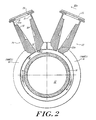
- FIG. 2 shows an illustrative embodiment of the present invention as a crossed-field amplifier 10 of generally cylindrical shape, in a view showing the electrode layout, with the anode 16 indicated schematically, without specifically illustrating the radially-oriented vanes of the slow wave circuit.
- the input and output matching transformers 23, 24 are shown, having ramped profiles to efficiently match the external waveguides to the narrow slots 23a, 24a where energy is coupled into and out of the interaction region or traveling wave space, peripheral gap 15.
- CFA 10 has a generally cylindrical cathode 14.
- each of the inlet and outlet transformers is covered by a ceramic window 25, 26 which is essentially transparent to the rf energy of interest and is sealed by brazing to the end to maintain vacuum inside the amplifier tube.
- a crossed field amplifier tube may employ somewhat varied overall architectures, and dimensions will vary depending upon the wavelengths to be amplified as well as the intended power and operating cycles.
- the present invention contemplates microwave or millimeter wave signals, having frequency between 450 MHz and about 35 Ghz, and operating at high power levels during switched time intervals, with an overall duty cycle under about 5%.
- a central support 12 carries a cylindrical cathode 14 which is spaced across a gap 15 from the inner diameter wall of the anode structure 16.
- the cathode is preferably made of a cold secondary emission type material such as beryllium or platinum.
- the device may, have an outer diameter of approximate ten centimeters, with a cathode OD of about seven centimeters and a height of approximately four centimeters.
- the structure of a corresponding S-band or shorter wavelength device may differ, and have generally smaller dimensions although generally requiring higher magnetic field strengths, for example in the range of 2500 Gauss.
- the cathode is carried by a ceramic support structure, with supporting conductors of copper or other suitable metal. Copper may also be used for the input and the output transformers 23, 24.
- anode 16 is maintained at ground potential, while the cathode is set negative, so that electrons are drawn from the surface of the cathode into the gap 15.
- the entire assembly is maintained in a permanent magnet package or solenoid (not shown) which provides the strong magnetic field in the gap 15 with lines perpendicular to the electric field.
- Electrons emitted from the cathode 14 are accelerated radially outward because of the voltage potential between the cathode 14 and the anode 16. If there is no rf drive power, the perpendicular (axial) magnetic field will cause the electrons to cycloid back to the cathode surface since the interaction space 15 is normally operated at a voltage below cut-off. However, when rf drive power is present, electrons emitted from the cathode 14 are sorted into two groups. The first group of electrons, known as the favorable phase electrons, give up dc potential energy to the rf wave. These electrons are collected at the anode 16.
- the second group of electrons absorb some energy from the rf wave on the anode circuit. With this additional energy, these electrons are driven back into the surface of cathode 14 with several hundred electron volts of energy.
- the cathode 14 emits new electrons with a yield ⁇ by secondary emission.
- ⁇ is typically sufficiently greater than one, so a dense region of electrons is maintained near the surface of the cathode 14; this dense region of electrons is usually referred to as the hub.
- the material of the cathode 14 has a secondary yield greater than two so that maintaining the hub is not a problem.
- the amount of dc energy given to the rf wave on the anode circuit by the favorable phase electrons more than offsets the amount of energy absorbed by unfavorable phase electrons, and hence there is a net rf amplification of the rf circuit wave on the anode 16.
- the device amplifies the input rf drive power, so the outlet 24 receives a greatly increased rf power.
- a control electrode may occupy a partial circumference of the cylinder, for example, located in the region of the inlet and outlet rf ports, and away from the traveling wave interaction area which makes up the major portion of the circumference of the device.
- the present invention is intended primarily for applications wherein the cathode/anode voltage is itself switched, and it addresses the multipactor effects of such switching operation.
- a high powered device may operate with relatively fast switching and a low, e.g., 1%-5% , duty cycle, but is vulnerable to multipactor effects which increase the noise level and are more severe with lower magnetic field strengths.
- the surface oxide films causing the multipactor discharge build up gradually during the lifetime of the crossed-field device. This build up is due to oxidation of exposed copper and/or to sputtered deposition of beryllium oxide or other secondary electron emitting material from the cathode.
- the oxidation and sputtering mechanisms are present due to the oxygen needed to maintain cathode emission or the oxides employed on the cathode for their high ⁇ . While the resulting discharge may be weak and introduce only a small amount of attenuation of the RF signal, fluctuation of the discharge is a significant source of noise close to the carrier. This fluctuating discharge limits the noise performance of the crossed-field device.
- the irregular firing or multipactor effects may be substantially reduced and allow operation with lower noise, or at magnetic field strengths approximately one half of those currently employed, by employing a grooved ceramic window in the rf signal path in combination with one or more other modifications of a surface region in the interior of the tube to reduce emissions.
- a grooved window for reducing multipactor in microwave tubes such as klystrons is diclosed in US3441784 .
- both the input and output windows are grooved, and the grooves form a regular array extending across the central region of the window.
- Figures 3A and 3B illustrate one suitable embodiment of such a window 29 which may for example function as the input window 25 or/and the output window 26 of the device of Figure 2 .
- window 29 has grooves 28 which extend in parallel across the face of the window. Preferably the array extends entirely across the face and thus covers the entire area, although for convenience of illustration only some of the grooves are shown in Figure 3A.
- Figure 3B illustrates a section taken transverse to the plane of the window 29 as used in an S-band crossed-field amplifier embodiment. As shown, the grooves extend close to each other and have width, depth and spacing dimensions which are all comparable. In the exemplary embodiment for a window employed on an S-band device, the groove spacing, width, and depth were each 0,25 mm (10 mils).
- the grooves were formed by machining with a thin diamond saw blade to form closely-spaced, parallel, straight-walled trenches, and the machined window was then cleaned, metallized and brazed to its mounting structure.
- the grooved side of the window faces inwardly, toward the interior of the amplifier tube 10.
- the window itself was formed of beryllia or other ceramic, and was a disk about 8,9 cm (3.5 inches) in diameter and an eighth of 2,5 cm (an inch) thick.
- the crossed-field amplifier of the present invention includes one or more interior surfaces of the amplifier assembly and or transformers having a physical structure or surface material modified to reduce or suppress multipactor, or its trigger events.
- the anode is sputter coated with a molybdenum oxide layer to inhibit such discharge.
- the coating may be effected by sputtering molybdenum in an oxidizing atmosphere, and the oxide deposition is carried out to deposit a thin sputtered layer, with thickness much less than the rf skin depth and which thus does not affect the attenuation of the circuit.
- Applicant has found that the effectiveness of this molybdenum oxide coating may diminish over time due to sputtering of the beryllium oxide or other secondary electron emitting material from the cathode. This may occur over the course of a relatively short period of amplifier operation, on the order of tens of hours.
- This aging of the anode coating is addressed in a further embodiment of the invention by embedding molybdenum wire, disk, or strip areas 35 in the surface of the cathode 14 as shown in the cross-sectional view of Figure 5 .
- the exposed molybdenum areas 35 cover only a minor area of the cathode, leaving the basic electron-generating mechanism unimpaired, but the area 35 is made large enough so that molybdenum is sputtered from those exposed areas to poison, coat or otherwise suppress the emission properties of the sputtered secondary-emitting material accreting on the anode, and to preserve the discharge suppression properties of the original molybdenum oxide anode coating.
- grooved window construction wherein major wall portions or metallic or oxidized surfaces of major components within the active signal path in the amplifier are grooved to further reduce secondary emissions.
- major surfaces in the input or output transformers 23, 24 are preferably provided with grooving, which may be similar to the grooves applied in some other microwave tubes to reduce secondary yield.
- Figures 4A and 4B further illustrate the geometric structure of one suitable transformer which, for purposes of illustration will be taken to be the output transformer 24 of Figure 2 .
- transformer 24 extends from the output rf iris, slot 24a of the amplifier tube 10, and includes an elongated ramp 50.
- Figure 4A shows a plan view parallel to the center line of the device in a plane extending through the rf aperture and perpendicular to the plane of the drawing in Figure 2 .
- the window is indicated schematically by 29, and the rf iris or slot is indicated generally at region 28.
- the transformer body itself may be composed of two identical shell portions symmetric about the center line to form a generally rectangular signal conduit having internally-protruding walls to shape and guide the desired single-mode signal between the amplifier and an external waveguide, which is generally multi-node.
- the transformer body includes a major ramp surface 50 running between the large window 29 and the rf iris of the crossed-field device.
- Surface 50 runs from a broad end at an initial step 51 centrally aligned with the position of the external waveguide, and extends inward from each side as a sloping wall decreasing in width as it slopes inward of the center plane of the assembly to a flat face 52 close to the center plane at the rf iris of the amplifier.
- 7.94 milled flats 53a, 53b on the wings of the ramp further define and tailor the transformer impedance or transfer characteristics.
- FIG. 4B shows a plan view of the two assembled halves of the transformer aligned parallel to the major axis of the rf aperture and the waveguide, as viewed from the window 29 looking inward toward the amplifier tube 10.
- Figure 4B shows a plan view of the two assembled halves of the transformer aligned parallel to the major axis of the rf aperture and the waveguide, as viewed from the window 29 looking inward toward the amplifier tube 10.
- various other unlabeled bounding walls also define the peripheral space along the signal path, and these shall be referred to generally herein simply as transformer body or housing walls.
- grooves are provided in the metal surface of one or more of these major signal guiding walls in the input and/or output transformer.
- surface 50, surface 52, surfaces 53a and 53b, as well as the vertical surfaces bounding the major portion of ramp 50 and the interior body or housing walls of the transformer may each be provided with grooves.
- the grooving may run parallel to the direction of signal propagation or transversely, and is generally dimensioned so as to not introduce unwanted resonance or interference effects in the underlying signals, but to effectively trap secondary electrons and/or decrease the area from which secondary electrons may be emitted along trajectories that enter the signal path.
- grooves may be generally suitable for transformer surfaces of the present invention.
- the input and output transformers reside generally in a peripheral region about the amplifier, in which the magnetic field is a fringing field of lesser strength than in the interaction region 15 between the cathode and anode of the amplifier tube itself.
- the spacing or dimensions of the grooves or their orientation so as to more effectively assure that secondary emissions occurring along the treated region are trapped within the grooves or do not affect tube operation or contribute noise to the output signal.
- the grooving may take various dimensions and orientations, and be positioned in such locations as may be effective to reduce the secondary electron yield of the surface and lower the noise level or operate stably with reduced magnetic fields in practice.
- the invention contemplates operation with a grooved window and chemical treatment or physical structure embodied in the walls of at least one major operating portion of the device or its transformers.
- the combination of two or more of the wall stabilizing or suppressing features is especially preferred for enhanced noise reduction and extended operation with lower noise and/or at lower magnetic field strengths, which may for example be dependably reduced by as much as one half.
Landscapes
- Microwave Tubes (AREA)
- Microwave Amplifiers (AREA)
Description
- The present invention relates to pulsed or intermittently operated crossed-field devices such as crossed field amplifiers (CFAs). By way of example, United States Patent
3,255,422 shows one such CFA device wherein a microwave entry waveguide provides radio frequency energy to an entry port for a slow wave propagating structure on an anode. A cathode is opposed to this anode across a gap. A solenoid provides a strong magnetic field perpendicular to the applied electric field. The cathode is formed of a material having a secondary emission ratio greater than unity so that electrons emitted from the cathode due to the electric field follow re-entrant trajectories in the magnetic field and bombard the cathode to cause further electron emission. Energy exchange between the emitted electrons and the rf field results in amplification of the input signal, which is then coupled through an outlet port as an amplified signal into a waveguide. - In some applications, a CFA is designed to operate with the anode and cathode always energized, and a pulsed input signal is applied to the inlet port and amplified as it travels to the outlet. In that case, because the cathode is formed of a material selected to readily emit secondary electrons, such devices, if not provided with a means for shutting down the electron emission, may continue to run spontaneously even when the input signal is removed. Thus, for those devices, it is customary to provide a control electrode as set forth in the aforesaid
U.S. Patent No. 3,255,422 which during a turn-off phase is pulsed near anode potential to capture electrons and thus end the secondary electron re-emission. Other methods of assuring shut-down for these pulsed-input devices may utilize specialized constructions, such as the second anode structure described inU.S. Patent Application 09/259,643 : (US6236161, published 22 May 2001 ). Other applications of CFAs operate by switching the anode/cathode potential on and off. These latter CFAs operate without such a control electrode structure, but are subject to multipactor effects from the high voltage switching cycles. - In general, when these devices are operated for example as high-power radar tubes, they are operated with extremely high powers but low duty cycles, thus requiring them to be switched on and off at high speeds. The nature of the crossed-field amplifier, requiring large secondary electron emissions, makes it particularly susceptible to multipactor and other gas discharge effects during such switching, and the multipactor effects are particularly pronounced with lower magnetic fields.
- Some potential advantages of using a low magnetic field have been recognized since the early days of magnetron and crossed-field amplifier development. However, in general, for high power amplifier as described above, it has been necessary to employ relatively high magnetic fields in order to avoid multipactor and sustain clean operation and switching. The field strength is typically several thousand Gauss in the interaction region of an S-band device operating at 150 to 300 kilowatts peak power, and somewhat lower at the surfaces and lead-in portions of the amplifier outside the interaction space where many multipactor effects are sustained. The ability to operate a high powered microwave or millimeter wave device with a lower magnetic field would offer advantages in terms of physical weight as well as operation and signal quality.
- The presence of multipactor and gas discharge effects on the anode circuit and elsewhere within the device has been recognized as a significant problem arising with a low magnetic field. One existing theory suggests an approach to overcome this problem by simply employing a magnetic field which exceeds the cyclotron value to suppress discharges perpendicular to the magnetic field (i.e., between anode vanes). However, applicant's initial attempt to implement such a solution with a magnetic field operating at a strength slightly above the cyclotron value showed that while discharges between vanes exist mainly below the cyclotron resonance field, they extend above this value to an extent which can interfere with the performance of the cross-field amplifier. The physics of this process is complex. Ordinarily, secondary emission occurs on a time scale orders of magnitude less than an rf cycle. The cyclotron resonance multipactor cut-off depends on this property. Both analysis and experiment suggest that the discharges above the cyclotron resonance field result from an ability of oxidized surfaces with insulating properties to store charge generated by incident primary electrons for an appreciable fraction of an rf cycle, and to subsequently emit this charge when the rf field reverses. The emission is a form of thin-film field emission, but its result is the same as, or may be modeled as, a secondary emission with time delay having a duration which is significant relative to the duration of an rf cycle. Reference to this effect in the literature employs the term "time-delayed secondary emission". Unfortunately, oxides are necessary components to achieve the high yield of secondary electrons upon which the traveling wave amplification effects depend, and the harsh conditions within the interaction space operate to transport these, or produce other, oxides. Given the presence of such oxides, it would appear that, at present, only very high magnetic fields can effectively eliminate multipactor.
- Accordingly, it would be desirable to provide such a device that operates dependably without multipactor at lower magnetic field strengths.
- According to an aspect of the present invention, there is provided a crossed-field device as specified in
claim 1. - The present invention overcomes deficiencies of known devices by providing a crossed-field device such as a crossed-field amplifier or magnetron wherein a distributed cathode body is spaced from an anode to provide an electric field in a slow wave region or interaction space, which, in a crossed-field device, extends for example between a signal inlet and an outlet, and the slow wave region is arranged to have a magnetic field oriented perpendicular to the electric field to enhance generation of secondary electrons. At least one window, and in an amplifier preferably both of the output and input windows to the amplifier tube, are formed with a closely spaced set of grooves over the window surface, and at least one other major surface component of the assembly is grooved, coated or is otherwise configured to further inhibit secondary electron emission or delayed emission.
- In a preferred embodiment the windows are formed of ceramic or material transparent to radiation, and have a regular array of parallel grooves approximately 0,25 mm (ten mils) wide and ten mils deep on a ten mil spacing. The amplifier may possess a cathode of secondary emitting material, such as beryllium, and secondary emission may be inhibited on the anode surface by providing a molybdenum oxide coating. Alternatively, or in addition, the cathode may have molybdenum wires, strips or segments included in a portion of its surface area to provide a reservoir or source of material that supplies the anode with sputtered or vaporized molybdenum during operation to maintain its operating characteristics. The grooved window may also be employed in conjunction with grooving of some or all of the major surfaces of the input and/or output transformers.
- These and other features of the invention will be understood from the description below taken together with the drawings wherein:
-
Figures 1, 1A and1B illustrate crossed field amplifier (CFA) devices of the prior art; -
Figure 2 is a cross-sectional view, partly schematic, of one embodiment of a device of the present invention; -
Figure 3A and 3B show windows of the embodiment ofFigure 2 ; -
Figure 4A and 4B illustrate the input/output transformers of another embodiment, and -
Figure 5 illustrates cathode construction of another embodiment. -
Figure 1 illustrates an external perspective view of a representative crossed-field amplifier device 1 of the prior art. As shown, the crossed-field amplifier device includes aninlet port 3 for providing input microwave energy into a body 2, where it is amplified by the crossed-field interaction as it travels to anoutlet 4 which carries the amplified energy away. A crossed-field amplifier (CFA) tube can be described as part magnetron and part traveling wave tube. Like a magnetron it utilizes crossed electric and magnetic fields to produce rf energy from emitted electrons. Like a traveling wave tube (TWT) the electrons interact with a traveling wave, and the device is an amplifier. Power is generated with high efficiency for the same reasons that a magnetron operates efficiently; power is also generated at voltage levels similar to those of a magnetron, i.e., many kilovolts. As shown inFigure 1 , a CFA may look quite like a magnetron, with the same form factor but with the addition of an input port. -
Figure 1A schematically represents the elements and operation of one CFA. The CFA device includes a slow wave circuit, an input/output system, and an electronics system. The slow wave circuit, or delay line as it sometimes called, is a periodic structure which has the circuit characteristics of a band-pass filter. This may be implemented by a regular set of radially oriented vanes, that extend inwardly, for example, from a surrounding circumferential anode structure. The slow wave circuit propagates rf energy over the frequency range of interest while providing fringing electric field lines with which electrons may interact. These fields must have a phase velocity approximately equal to the velocity of the electron stream. The input/output system provides an impedance transformation between the rf transmission line system external to the amplifier, and the slow wave circuit itself. For microwave signals, this may involve a tapered chamber, which extends from the vacuum sealing ceramic window at the external wave guide to a narrow slot-like entry port or passage at the interaction space. These impedance transformations or circuit matches may determine the useful bandwidth of the CFA itself. The electronics system generates electrons, and confines them to the interaction area, i.e., to the slow wave circuit, where they give up energy to the rf field and thus "amplify" the input energy. The electronics system also collects electrons when they are spent. Some CFAs have a relatively large cathode which extends the entire length of the slow wave circuit. In these CFAs, electrons are generated along the entire length of the cathode, giving rise to the name "distributed emission amplifier". The cathode is also called the sole, from which the name "emitting sole amplifier" has arisen. - The distributed emission amplifier can be arranged in a number of ways. It can be made in either a linear or a circular architecture. Amplifiers made with the circular format may collect electrons at one end of the circuit, or the input and output sections may be brought close enough together so that the electrons from the output are permitted to continue along and re-enter the interaction area at the input. Re-entrance is employed in many amplifiers to enhance efficiency. When re-entrance is employed, however, it is possible that re-entering electrons may be modulated with information that will subsequently be amplified. This is equivalent to providing an rf feedback, and this feedback must be considered in determining the behavior of the amplifier. It is also possible to obtain re-entrance after demodulating the electron stream to eliminate such rf feedback.
- CFAs are mostly used for high-power applications, as opposed to small signal use, and the slow wave circuit must be capable of dissipating the collected beam and transferring that energy to a heat sink. A typical use, for example, is as a broad band phase stable microwave amplifier for a coherent radar chain, to efficiently generate very high peak output power from a relatively low input voltage which can be either applied to the cathode or to an electrode similar to a TWT cathode, or may operate by grid pulsing. Such CFAs may be produced in small lightweight packages. The invention will be described below with respect to an essentially cylindrical arrangement of opposed cathode and anode elements in which the traveling wave or interaction region occupies a major portion of the circumference, between the inlet port and the outlet port. However, the construction of the invention may also be implemented in other distributed emission devices, such as magnetrons. In the prior art device of
Figure 1A , a control electrode segment separate from the cathode may be pulsed to shut down amplifier operation in synchrony with the trailing edge of a pulsed input signal, while the cathode and anode potentials remain unchanged. In the prior art device ofFigure 1B , no control electrode is provided, and the cathode/anode potential is changed to interrupt the output signal. This high voltage switching is vulnerable to multipactor effects that increase the noise level of the output. -
Figure 2 shows an illustrative embodiment of the present invention as a crossed-field amplifier 10 of generally cylindrical shape, in a view showing the electrode layout, with theanode 16 indicated schematically, without specifically illustrating the radially-oriented vanes of the slow wave circuit. The input andoutput matching transformers narrow slots peripheral gap 15.CFA 10 has a generallycylindrical cathode 14. - The outer end of each of the inlet and outlet transformers is covered by a
ceramic window - It will be appreciated that the actual construction of a crossed field amplifier tube may employ somewhat varied overall architectures, and dimensions will vary depending upon the wavelengths to be amplified as well as the intended power and operating cycles. In general the present invention contemplates microwave or millimeter wave signals, having frequency between 450 MHz and about 35 Ghz, and operating at high power levels during switched time intervals, with an overall duty cycle under about 5%.
- As shown in
Figure 2 acentral support 12 carries acylindrical cathode 14 which is spaced across agap 15 from the inner diameter wall of theanode structure 16. The cathode is preferably made of a cold secondary emission type material such as beryllium or platinum. For a typical L-band amplifier, the device may, have an outer diameter of approximate ten centimeters, with a cathode OD of about seven centimeters and a height of approximately four centimeters. The structure of a corresponding S-band or shorter wavelength device may differ, and have generally smaller dimensions although generally requiring higher magnetic field strengths, for example in the range of 2500 Gauss. Typically the cathode is carried by a ceramic support structure, with supporting conductors of copper or other suitable metal. Copper may also be used for the input and theoutput transformers - For one typical device the outer structure,
anode 16 is maintained at ground potential, while the cathode is set negative, so that electrons are drawn from the surface of the cathode into thegap 15. The entire assembly is maintained in a permanent magnet package or solenoid (not shown) which provides the strong magnetic field in thegap 15 with lines perpendicular to the electric field. - Electrons emitted from the
cathode 14 are accelerated radially outward because of the voltage potential between thecathode 14 and theanode 16. If there is no rf drive power, the perpendicular (axial) magnetic field will cause the electrons to cycloid back to the cathode surface since theinteraction space 15 is normally operated at a voltage below cut-off. However, when rf drive power is present, electrons emitted from thecathode 14 are sorted into two groups. The first group of electrons, known as the favorable phase electrons, give up dc potential energy to the rf wave. These electrons are collected at theanode 16. The second group of electrons, the unfavorable phase electrons, absorb some energy from the rf wave on the anode circuit. With this additional energy, these electrons are driven back into the surface ofcathode 14 with several hundred electron volts of energy. As a result of this electron bombardment, thecathode 14 emits new electrons with a yield δ by secondary emission. δ is typically sufficiently greater than one, so a dense region of electrons is maintained near the surface of thecathode 14; this dense region of electrons is usually referred to as the hub. Typically, the material of thecathode 14 has a secondary yield greater than two so that maintaining the hub is not a problem. The amount of dc energy given to the rf wave on the anode circuit by the favorable phase electrons more than offsets the amount of energy absorbed by unfavorable phase electrons, and hence there is a net rf amplification of the rf circuit wave on theanode 16. - Thus, in overall operation, the device amplifies the input rf drive power, so the
outlet 24 receives a greatly increased rf power. - As shown in
Figure 1A , in other constructions a control electrode may occupy a partial circumference of the cylinder, for example, located in the region of the inlet and outlet rf ports, and away from the traveling wave interaction area which makes up the major portion of the circumference of the device. However, the present invention is intended primarily for applications wherein the cathode/anode voltage is itself switched, and it addresses the multipactor effects of such switching operation. - As described above, a high powered device may operate with relatively fast switching and a low, e.g., 1%-5% , duty cycle, but is vulnerable to multipactor effects which increase the noise level and are more severe with lower magnetic field strengths. The surface oxide films causing the multipactor discharge build up gradually during the lifetime of the crossed-field device. This build up is due to oxidation of exposed copper and/or to sputtered deposition of beryllium oxide or other secondary electron emitting material from the cathode. The oxidation and sputtering mechanisms are present due to the oxygen needed to maintain cathode emission or the oxides employed on the cathode for their high δ. While the resulting discharge may be weak and introduce only a small amount of attenuation of the RF signal, fluctuation of the discharge is a significant source of noise close to the carrier. This fluctuating discharge limits the noise performance of the crossed-field device.
- In accordance with a principal aspect of the present invention, applicant has found that the irregular firing or multipactor effects may be substantially reduced and allow operation with lower noise, or at magnetic field strengths approximately one half of those currently employed, by employing a grooved ceramic window in the rf signal path in combination with one or more other modifications of a surface region in the interior of the tube to reduce emissions. A grooved window for reducing multipactor in microwave tubes such as klystrons, is diclosed in
US3441784 . Preferably both the input and output windows are grooved, and the grooves form a regular array extending across the central region of the window. -
Figures 3A and 3B illustrate one suitable embodiment of such awindow 29 which may for example function as theinput window 25 or/and theoutput window 26 of the device ofFigure 2 . As shown,window 29 hasgrooves 28 which extend in parallel across the face of the window. Preferably the array extends entirely across the face and thus covers the entire area, although for convenience of illustration only some of the grooves are shown inFigure 3A. Figure 3B illustrates a section taken transverse to the plane of thewindow 29 as used in an S-band crossed-field amplifier embodiment. As shown, the grooves extend close to each other and have width, depth and spacing dimensions which are all comparable. In the exemplary embodiment for a window employed on an S-band device, the groove spacing, width, and depth were each 0,25 mm (10 mils). The grooves were formed by machining with a thin diamond saw blade to form closely-spaced, parallel, straight-walled trenches, and the machined window was then cleaned, metallized and brazed to its mounting structure. In use, the grooved side of the window faces inwardly, toward the interior of theamplifier tube 10. The window itself was formed of beryllia or other ceramic, and was a disk about 8,9 cm (3.5 inches) in diameter and an eighth of 2,5 cm (an inch) thick. - In addition to having one or more grooved windows, the crossed-field amplifier of the present invention includes one or more interior surfaces of the amplifier assembly and or transformers having a physical structure or surface material modified to reduce or suppress multipactor, or its trigger events.
- In one embodiment, the anode is sputter coated with a molybdenum oxide layer to inhibit such discharge. The coating may be effected by sputtering molybdenum in an oxidizing atmosphere, and the oxide deposition is carried out to deposit a thin sputtered layer, with thickness much less than the rf skin depth and which thus does not affect the attenuation of the circuit. Applicant has found that the effectiveness of this molybdenum oxide coating may diminish over time due to sputtering of the beryllium oxide or other secondary electron emitting material from the cathode. This may occur over the course of a relatively short period of amplifier operation, on the order of tens of hours.
- This aging of the anode coating is addressed in a further embodiment of the invention by embedding molybdenum wire, disk, or
strip areas 35 in the surface of thecathode 14 as shown in the cross-sectional view ofFigure 5 . The exposedmolybdenum areas 35 cover only a minor area of the cathode, leaving the basic electron-generating mechanism unimpaired, but thearea 35 is made large enough so that molybdenum is sputtered from those exposed areas to poison, coat or otherwise suppress the emission properties of the sputtered secondary-emitting material accreting on the anode, and to preserve the discharge suppression properties of the original molybdenum oxide anode coating. Using this molybdenum suppressor-regeneration construction in a prototype embodiment tested for over 3,000 hours at 1% duty cycle, the test noise level degraded only slightly at the lower end of the intended frequency band. Because oxygen pressure drops substantially over the first thousand hours of operation, and the rates of surface oxidation and oxide sputtering drop to very low levels, the effectiveness of exposed molybdenum to maintain the anode coating beyond the initial hours of operation of the CFA indicates a deposition rate that can be expected to remain effective over a much more extended period of operation. Thus, the molybdenum oxide coating on the anode is preserved and effective throughout the life of the tube. - In addition to such coating, applicant contemplates embodiments of the grooved window construction wherein major wall portions or metallic or oxidized surfaces of major components within the active signal path in the amplifier are grooved to further reduce secondary emissions. In particular, major surfaces in the input or
output transformers -
Figures 4A and 4B further illustrate the geometric structure of one suitable transformer which, for purposes of illustration will be taken to be theoutput transformer 24 ofFigure 2 . - As shown in
Figure 2 ,transformer 24 extends from the output rf iris,slot 24a of theamplifier tube 10, and includes anelongated ramp 50.Figure 4A shows a plan view parallel to the center line of the device in a plane extending through the rf aperture and perpendicular to the plane of the drawing inFigure 2 . The window is indicated schematically by 29, and the rf iris or slot is indicated generally atregion 28. The transformer body itself may be composed of two identical shell portions symmetric about the center line to form a generally rectangular signal conduit having internally-protruding walls to shape and guide the desired single-mode signal between the amplifier and an external waveguide, which is generally multi-node. - As shown, the transformer body includes a
major ramp surface 50 running between thelarge window 29 and the rf iris of the crossed-field device.Surface 50 runs from a broad end at aninitial step 51 centrally aligned with the position of the external waveguide, and extends inward from each side as a sloping wall decreasing in width as it slopes inward of the center plane of the assembly to aflat face 52 close to the center plane at the rf iris of the amplifier. In the illustrated embodiment of 7.94 milledflats Figure 4B , which shows a plan view of the two assembled halves of the transformer aligned parallel to the major axis of the rf aperture and the waveguide, as viewed from thewindow 29 looking inward toward theamplifier tube 10. Beyond the specifically numbered or identified surfaces of the ramps or steps forming the features of the transformer assembly, various other unlabeled bounding walls also define the peripheral space along the signal path, and these shall be referred to generally herein simply as transformer body or housing walls. - In accordance with this further aspect of the invention, grooves are provided in the metal surface of one or more of these major signal guiding walls in the input and/or output transformer. Thus,
surface 50,surface 52, surfaces 53a and 53b, as well as the vertical surfaces bounding the major portion oframp 50 and the interior body or housing walls of the transformer may each be provided with grooves. The grooving may run parallel to the direction of signal propagation or transversely, and is generally dimensioned so as to not introduce unwanted resonance or interference effects in the underlying signals, but to effectively trap secondary electrons and/or decrease the area from which secondary electrons may be emitted along trajectories that enter the signal path. To the extent grooves have been employed for emission reduction in microwave constructions in the past, such grooves may be generally suitable for transformer surfaces of the present invention. It will be understood that the input and output transformers reside generally in a peripheral region about the amplifier, in which the magnetic field is a fringing field of lesser strength than in theinteraction region 15 between the cathode and anode of the amplifier tube itself. It may in some circumstances be desirable to set the spacing or dimensions of the grooves or their orientation so as to more effectively assure that secondary emissions occurring along the treated region are trapped within the grooves or do not affect tube operation or contribute noise to the output signal. In general, the grooving may take various dimensions and orientations, and be positioned in such locations as may be effective to reduce the secondary electron yield of the surface and lower the noise level or operate stably with reduced magnetic fields in practice. - Thus the invention contemplates operation with a grooved window and chemical treatment or physical structure embodied in the walls of at least one major operating portion of the device or its transformers. The combination of two or more of the wall stabilizing or suppressing features is especially preferred for enhanced noise reduction and extended operation with lower noise and/or at lower magnetic field strengths, which may for example be dependably reduced by as much as one half.
- The invention being thus disclosed and representative embodiments thereof described, further variations and modifications will occur to those skilled in the art, and all such variations and modifications are considered to be within the scope of the invention, as set forth in the claims appended hereto and equivalents thereof.
Claims (10)
- A crossed-field device operable in a switched mode, such device including:an inlet (23) for accepting an input signal to said device for amplification, said inlet (23) having an inlet window (25);an outlet (24) for carrying an amplified signal from said device, said outlet (24) having an outlet window (26) and said device defining an active signal path between said inlet (23) and said outlet (24);a cathode body portion (14) having an emitter surface configured for secondary emission of electrons; andan anode portion (16) spaced about said cathode body portion (14) providing a gap (15) between said cathode body portion (14) and said anode portion (16); said cathode body portion (14) and said anode portion (16) providing an electric field in said gap (15) along an interaction slow wave traveling region wherein a crossed magnetic field in said slow wave traveling region cooperates to maintain emitted electrons on cycloidal pathways as they travel between said inlet (23) and said outlet (24);characterized in thatat least one of said inlet window (25) and said outlet window (26) is a grooved window (29); andsaid crossed-field device further comprises a surface region (35, 50, 52, 53a, 53b) internally disposed between said inlet (23) and said outlet (24) having a surface material structure that reduces secondary electron emission and operating in conjunction with said grooved window (29) so as to suppress multipactor during switched operation of said crossed-field device.
- A crossed-field device as claimed in claim 1, wherein said inlet (23) and said outlet (24) each include at least one signal guiding wall (50, 52, 53a, 53b) and said surface region (35, 50, 52, 53a, 53b) comprises a grooved surface formed in said at least one signal guiding wall (50, 52, 53a, 53b).
- A crossed-field device as claimed in claim 1 or claim 2, wherein said surface region (30, 50, 52, 53a, 53b) comprises a region (35) of the cathode (14) that includes a secondary emission material and exposed molybdenum wires, strips or segments at a surface thereof for enhancing multipactor suppression.
- A crossed-field device as claimed in claim 1 or claim 2, wherein said surface region comprises a region of the anode (16) that includes a molybdenum oxide coating for multipactor suppression.
- A crossed-field device as claimed in claim 4, wherein said cathode (14) includes surface exposed molybdenum wires, strips or segments.
- A crossed-field device as claimed in claim 2, wherein said anode (16) includes a molybdenum oxide coating.
- A crossed-field device as claimed in claim 2, wherein the cathode (14) includes molybdenum wires, strips or segments at an exposed surface thereof.
- A crossed-field device as claimed in claim 7, wherein the anode (16) includes a molybdenum oxide coating.
- A crossed-field device as claimed in any of claims 1-8, wherein said at least one grooved window (29) includes a regular array of parallel grooves extending across an rf aperture of said window, said grooves having a spacing, a width and a depth to effectively suppress multipactor and, preferably, wherein said grooves are approximately one-quarter millimeter wide and deep.
- A crossed-field device as claimed in any of claims 1-9, wherein said device is a crossed-field amplifier which, preferably operates with a low duty cycle in a switched mode.
Applications Claiming Priority (3)
| Application Number | Priority Date | Filing Date | Title |
|---|---|---|---|
| US11118298P | 1998-12-07 | 1998-12-07 | |
| US111182P | 1998-12-07 | ||
| PCT/US1999/028922 WO2000034976A1 (en) | 1998-12-07 | 1999-12-06 | Crossed-field amplifier with multipactor suppression |
Publications (3)
| Publication Number | Publication Date |
|---|---|
| EP1155434A1 EP1155434A1 (en) | 2001-11-21 |
| EP1155434A4 EP1155434A4 (en) | 2002-06-05 |
| EP1155434B1 true EP1155434B1 (en) | 2008-11-26 |
Family
ID=22337018
Family Applications (1)
| Application Number | Title | Priority Date | Filing Date |
|---|---|---|---|
| EP99961949A Expired - Lifetime EP1155434B1 (en) | 1998-12-07 | 1999-12-06 | Crossed-field amplifier with multipactor suppression |
Country Status (3)
| Country | Link |
|---|---|
| US (1) | US6437510B1 (en) |
| EP (1) | EP1155434B1 (en) |
| WO (1) | WO2000034976A1 (en) |
Cited By (1)
| Publication number | Priority date | Publication date | Assignee | Title |
|---|---|---|---|---|
| CN110165303A (en) * | 2019-06-10 | 2019-08-23 | 天津瑞晟晖能科技有限公司 | Secondary cell and preparation method thereof, electrical equipment |
Families Citing this family (3)
| Publication number | Priority date | Publication date | Assignee | Title |
|---|---|---|---|---|
| US6872929B2 (en) * | 2003-04-17 | 2005-03-29 | The Regents Of The University Of Michigan | Low-noise, crossed-field devices such as a microwave magnetron, microwave oven utilizing same and method of converting a noisy magnetron to a low-noise magnetron |
| US9147549B2 (en) | 2011-03-22 | 2015-09-29 | Communications & Power Industries Llc | Crossed-field amplifiers with anode/cathode structures for reduced spurious emissions |
| CN116526125B (en) * | 2023-06-27 | 2023-09-01 | 深圳市鑫龙通信技术有限公司 | Integrated radiating element, antenna and 5G dense antenna array |
Family Cites Families (7)
| Publication number | Priority date | Publication date | Assignee | Title |
|---|---|---|---|---|
| NL213139A (en) * | 1956-01-30 | |||
| US3069594A (en) * | 1959-11-27 | 1962-12-18 | Bell Telephone Labor Inc | Electron discharge devices |
| US3330707A (en) * | 1963-10-07 | 1967-07-11 | Varian Associates | Method for reducing electron multipactor on a dielectric window surface |
| US3441784A (en) * | 1967-04-26 | 1969-04-29 | Varian Associates | Ridged dielectric window with titanium suboxide solely on ridges |
| US4719436A (en) * | 1986-08-04 | 1988-01-12 | The United States Of America As Represented By The United States Department Of Energy | Stabilized chromium oxide film |
| US5196765A (en) * | 1988-07-05 | 1993-03-23 | Raytheon Company | High RF isolation crossed-field amplifier |
| US5548257A (en) * | 1995-09-18 | 1996-08-20 | The Regents Of The University Of California | Vacuum-barrier window for wide-bandwidth high-power microwave transmission |
-
1999
- 1999-12-06 EP EP99961949A patent/EP1155434B1/en not_active Expired - Lifetime
- 1999-12-06 US US09/455,886 patent/US6437510B1/en not_active Expired - Lifetime
- 1999-12-06 WO PCT/US1999/028922 patent/WO2000034976A1/en not_active Ceased
Cited By (1)
| Publication number | Priority date | Publication date | Assignee | Title |
|---|---|---|---|---|
| CN110165303A (en) * | 2019-06-10 | 2019-08-23 | 天津瑞晟晖能科技有限公司 | Secondary cell and preparation method thereof, electrical equipment |
Also Published As
| Publication number | Publication date |
|---|---|
| WO2000034976A1 (en) | 2000-06-15 |
| EP1155434A4 (en) | 2002-06-05 |
| EP1155434A1 (en) | 2001-11-21 |
| US6437510B1 (en) | 2002-08-20 |
Similar Documents
| Publication | Publication Date | Title |
|---|---|---|
| US20110006678A1 (en) | Hollow beam electron gun for use in a klystron | |
| CN100369178C (en) | Ion pump with secondary magnetic field | |
| US6437510B1 (en) | Crossed-field amplifier with multipactor suppression | |
| CA1136691A (en) | Electron tube with reduced secondary emission | |
| Lee et al. | A fifty megawatt klystron for the stanford linear collider | |
| US3123735A (en) | Broadband crossed-field amplifier with slow wave structure | |
| US7230385B2 (en) | Collector arrangement | |
| GB2440036A (en) | Travelling-wave tube with integrated ion trap power supply | |
| EP0227463B1 (en) | Secondary emission cathode and tube | |
| US6984940B2 (en) | Electronic tube with simplified collector | |
| US6872929B2 (en) | Low-noise, crossed-field devices such as a microwave magnetron, microwave oven utilizing same and method of converting a noisy magnetron to a low-noise magnetron | |
| CN114005718A (en) | A slow-wave structure of a connecting rod stepped symmetrical split ring | |
| US4608520A (en) | Cathode driven crossed-field amplifier | |
| RU2150765C1 (en) | Method and device for producing broad-band, high- power, superhigh-frequency quasi-noise signals | |
| US6236161B1 (en) | Crossed-field device | |
| Faillon | Klystrons and related devices | |
| McCune | Ion oscillation considerations for pulsed klystron amplifiers | |
| US7459855B2 (en) | Low-spurious-radiation microwave tube | |
| Theiss | LITTON HIGH-POWER FOLDED-WAVEGUIDE KA-BAND TWTS | |
| KR0139336Y1 (en) | Multi Beam Vacuum Tube | |
| US5874806A (en) | Passive jitter reduction in crossed-field amplifier with secondary emission material on anode vanes | |
| Luiz | A comprehensive review of travelling-wave tube technology | |
| KR0122675Y1 (en) | klystron | |
| JP3502512B2 (en) | Cathode structure of electromagnetic field orthogonal type amplification tube | |
| JPH0345858B2 (en) |
Legal Events
| Date | Code | Title | Description |
|---|---|---|---|
| PUAI | Public reference made under article 153(3) epc to a published international application that has entered the european phase |
Free format text: ORIGINAL CODE: 0009012 |
|
| 17P | Request for examination filed |
Effective date: 20010709 |
|
| AK | Designated contracting states |
Kind code of ref document: A1 Designated state(s): AT BE CH CY DE DK ES FI FR GB GR IE IT LI LU MC NL PT SE Kind code of ref document: A1 Designated state(s): FR |
|
| A4 | Supplementary search report drawn up and despatched |
Effective date: 20020424 |
|
| AK | Designated contracting states |
Kind code of ref document: A4 Designated state(s): FR |
|
| RIC1 | Information provided on ipc code assigned before grant |
Free format text: 7H 01J 25/42 A, 7H 01P 1/08 B, 7H 01J 25/50 B, 7H 01J 23/02 B |
|
| REG | Reference to a national code |
Ref country code: DE Ref legal event code: 8566 |
|
| 17Q | First examination report despatched |
Effective date: 20030626 |
|
| RBV | Designated contracting states (corrected) |
Designated state(s): FR |
|
| GRAP | Despatch of communication of intention to grant a patent |
Free format text: ORIGINAL CODE: EPIDOSNIGR1 |
|
| GRAS | Grant fee paid |
Free format text: ORIGINAL CODE: EPIDOSNIGR3 |
|
| GRAA | (expected) grant |
Free format text: ORIGINAL CODE: 0009210 |
|
| AK | Designated contracting states |
Kind code of ref document: B1 Designated state(s): FR |
|
| PLBE | No opposition filed within time limit |
Free format text: ORIGINAL CODE: 0009261 |
|
| STAA | Information on the status of an ep patent application or granted ep patent |
Free format text: STATUS: NO OPPOSITION FILED WITHIN TIME LIMIT |
|
| 26N | No opposition filed |
Effective date: 20090827 |
|
| REG | Reference to a national code |
Ref country code: FR Ref legal event code: PLFP Year of fee payment: 17 |
|
| REG | Reference to a national code |
Ref country code: FR Ref legal event code: PLFP Year of fee payment: 18 |
|
| REG | Reference to a national code |
Ref country code: FR Ref legal event code: PLFP Year of fee payment: 19 |
|
| PGFP | Annual fee paid to national office [announced via postgrant information from national office to epo] |
Ref country code: FR Payment date: 20181226 Year of fee payment: 20 |