EP1153697A2 - Method and apparatus for cutting a semiconductor wafer - Google Patents
Method and apparatus for cutting a semiconductor wafer Download PDFInfo
- Publication number
- EP1153697A2 EP1153697A2 EP01111061A EP01111061A EP1153697A2 EP 1153697 A2 EP1153697 A2 EP 1153697A2 EP 01111061 A EP01111061 A EP 01111061A EP 01111061 A EP01111061 A EP 01111061A EP 1153697 A2 EP1153697 A2 EP 1153697A2
- Authority
- EP
- European Patent Office
- Prior art keywords
- semiconductor wafer
- cut
- mount tape
- wafer
- resin base
- Prior art date
- Legal status (The legal status is an assumption and is not a legal conclusion. Google has not performed a legal analysis and makes no representation as to the accuracy of the status listed.)
- Granted
Links
Images



Classifications
-
- H—ELECTRICITY
- H10—SEMICONDUCTOR DEVICES; ELECTRIC SOLID-STATE DEVICES NOT OTHERWISE PROVIDED FOR
- H10P—GENERIC PROCESSES OR APPARATUS FOR THE MANUFACTURE OR TREATMENT OF DEVICES COVERED BY CLASS H10
- H10P95/00—Generic processes or apparatus for manufacture or treatments not covered by the other groups of this subclass
-
- B—PERFORMING OPERATIONS; TRANSPORTING
- B23—MACHINE TOOLS; METAL-WORKING NOT OTHERWISE PROVIDED FOR
- B23K—SOLDERING OR UNSOLDERING; WELDING; CLADDING OR PLATING BY SOLDERING OR WELDING; CUTTING BY APPLYING HEAT LOCALLY, e.g. FLAME CUTTING; WORKING BY LASER BEAM
- B23K26/00—Working by laser beam, e.g. welding, cutting or boring
- B23K26/18—Working by laser beam, e.g. welding, cutting or boring using absorbing layers on the workpiece, e.g. for marking or protecting purposes
-
- B—PERFORMING OPERATIONS; TRANSPORTING
- B23—MACHINE TOOLS; METAL-WORKING NOT OTHERWISE PROVIDED FOR
- B23K—SOLDERING OR UNSOLDERING; WELDING; CLADDING OR PLATING BY SOLDERING OR WELDING; CUTTING BY APPLYING HEAT LOCALLY, e.g. FLAME CUTTING; WORKING BY LASER BEAM
- B23K26/00—Working by laser beam, e.g. welding, cutting or boring
- B23K26/14—Working by laser beam, e.g. welding, cutting or boring using a fluid stream, e.g. a jet of gas, in conjunction with the laser beam; Nozzles therefor
- B23K26/146—Working by laser beam, e.g. welding, cutting or boring using a fluid stream, e.g. a jet of gas, in conjunction with the laser beam; Nozzles therefor the fluid stream containing a liquid
-
- H—ELECTRICITY
- H10—SEMICONDUCTOR DEVICES; ELECTRIC SOLID-STATE DEVICES NOT OTHERWISE PROVIDED FOR
- H10P—GENERIC PROCESSES OR APPARATUS FOR THE MANUFACTURE OR TREATMENT OF DEVICES COVERED BY CLASS H10
- H10P54/00—Cutting or separating of wafers, substrates or parts of devices
Definitions
- the present invention relates to a method and an apparatus for cutting a semiconductor wafer and, more particularly to a method and an apparatus for cutting a semiconductor wafer, adhered to a mount tape, into individual pieces by a cutter.
- a semiconductor element used for a semiconductor device is supplied by cutting a silicon wafer 12 (hereinafter referred merely to a "wafer" 12), on which a plurality of semiconductor elements 13 are formed, into individual pieces.
- a back surface of the wafer 12 is adhered to a mount tape 100 mainly composed of a resin with an adhesive layer 14, as shown in Fig. 8.
- the mount tape 100 on which the wafer 12 is adhered is placed on a stage surface of a stage 102 and cut with a rotating blade 104 as shown in Fig. 9, wherein a predetermined gap H is maintained between the stage surface of the stage 102 and the rotating blade 104.
- cut grooves 106 are formed by the rotating blade 104. While the semiconductor elements 13 of the wafer 12 are separated from each other by the cut grooves 106, the mount tape 100 is not completely cut and individual cut semiconductor elements are still adhered to the mount tape. Therefore, the cut semiconductor elements 13 are prevented from scattering during and/or after cutting, whereby the cutting operation and the post treatment are facilitated.
- the thickness of the wafer 12 has recently been reduced, resulting in a lowering of wafer strength. Thereby, it has been found that cracks or chipped portions are generated in the wafer 12 when cut by the rotating blade 104.
- the inventors of the present invention believe that such cracks or chipped portions are caused by a shearing force applied to the wafer 12 when the wafer 12 is cut by the rotating blade 104, and have tried to cut the wafer 12 with a laser beam.
- the inventors of the present invention have found that, if the laser beam is used for cutting the wafer 12 into individual semiconductor elements 13, the mount tape 100 is also cut into pieces.
- the inventors then tried to cut the semiconductor elements 13 on the wafer 12 into individual pieces and half-cut the mount tape 100 with a laser beam, and found that it is necessary to delicately adjust an output of the laser beam if a desirable cut groove 106 as shown in Fig. 10 is to be formed and that the heat generation is problematic in the cutting of wafer with the laser beam, which means that the cutting of the wafer 12 with the laser beam is not industrially advantageous.
- this method is advantageous because it is free from the generation of cracks and/or chipped portions caused by the cutting of wafer 12, since no large shearing force is applied onto the wafer 12 unlike the cutting with the rotating blade 104.
- An object of the present invention is to provide a method for easily cutting a wafer with a laser beam.
- the present inventors have studied the above-mentioned problems of the prior art and found that it is possible to cut the wafer while removing heat generated in a cut area during the cutting operation, if the laser beam cutter ejects a beam-like water jet having a predetermined width corresponding to a slit to be cut to an area of the wafer to be cut, while directing a laser beam axially through the beam-like water jet.
- the inventors have found that, by using a mount tape in which is embedded a mesh-like member formed of material harder than a main resin component of the mount tape, it is possible, even though the mount tape is cut into pieces, to prevent the individual cut pieces from scattering about because the mesh-like member is not cut and connects the cut pieces with each other. Thus, the present invention was completed.
- a method for cutting a semiconductor wafer comprising the following steps of: adhering a mount tape on a back surface of said semiconductor wafer, said mount tape comprising a resin base and a mesh-like member made of a material harder than that of said resin base and embedded in said resin base; and ejecting a beam-like liquid jet toward a front surface of said semiconductor wafer and simultaneously transmitting a laser beam axially through said beam-like liquid jet, so that said semiconductor wafer is cut into individual pieces by said laser beam together with said resin base of the mount tape, while said mesh-like member remains in its connected state.
- the pressure of said beam-like liquid jet and the output of said laser beam is determined in such a manner that said semiconductor wafer is sufficiently cut, while the mesh-like member of the mount tape is not cut, but remains in its connected state.
- a liquid beam having a width corresponding to a desired slit width to be cut is ejected on an area of a wafer to be cut and, simultaneously a laser beam is axially directed through the beam-like liquid to the area of the wafer to be cut, it is possible to remove heat, generated during the cutting with the laser beam, by the beam-like liquid, as well as to minimize the shearing force applied to the wafer in comparison with a case wherein the wafer is cut with a rotating blade.
- an assembly of a wafer adhered to a mount tape in which is embedded a mesh-like member formed of material harder than a main resin component of the mount tape is cut with a laser beam transmitted axially through the beam-like liquid jet ejected to have a width corresponding to a desired slit width to be cut.
- the mesh-like member connects the individually cut pieces with each other to prevent the cut pieces from being scattered about. As a result, the cutting operation and the post treatment can easily be carried out.
- the beam-like liquid jet is a pressurized pure water jet and focused so as to have a diameter in a range of 30 to 50 ⁇ m, so that said semiconductor wafer cuts along a slit having a corresponding width.
- the said mesh-like member is a glass cloth made of glass filament.
- the glass cloth comprises a plurality of lateral filaments and a plurality of transverse filaments substantially extending perpendicularly to the lateral filaments, so that the semiconductor wafer is cut along a slit which extends so as not to be in parallel to said lateral or said transverse filaments.
- the semiconductor wafer is preferably cut along a slit which extends at an angle of 30 to 60 degree to said lateral and said transverse filaments.
- a total thickness of the mount tape is in a range from 80 to 100 ⁇ m and a diameter of the glass fiber is in a range from 20 to 90 ⁇ m.
- an apparatus for cutting a semiconductor wafer comprising: a mount tape comprising a resin base and a mesh-like member made of a material harder than that of the resin base and embedded in the resin base; first means for holding the mount tape, to which a back surface of the semiconductor wafer is adhered, second means for ejecting a beam-like liquid jet toward a front surface of the semiconductor wafer and simultaneously transmitting a laser beam axially through the beam-like liquid jet; and means for moving at least one of the first and second means, so that the semiconductor wafer is cut into individual pieces by the laser beam together with the resin base of the mount tape, while the mesh-like member remains in its connected state.
- a mount tape 10 used in the present invention is mainly made of polyimide resin 16 and has a mesh-like member 18 formed of a material harder than the resin.
- the mesh-like member shown in Fig. 1 is a glass cloth 18 formed of glass filaments.
- the glass cloth 18 is woven with glass filaments in a plain weave. Such a glass cloth 18 is embedded horizontally all over the mount tape 10 and generally at a central position in the thickness direction thereof.
- a back surface of a wafer 12 is adhered via an adhesive layer 14 to one surface of the mount tape 10 carrying the glass cloth 18.
- the adhesive layer 14 is composed of an ultraviolet-curing resin.
- glass cloth 18 exists all over the mount tape 10 in the embodiment shown in Fig. 1, it may be provided solely in an area where the wafer 12 is to be adhered.
- the mount tape 10 may be mainly composed of an ultraviolet-curing resin.
- the wafer 12 can be adhered with the same ultraviolet-curing resin as that of the mount tape 10.
- the assembly of the wafer 12 and the mount tape 10 shown in Fig. 1 is cut by using a laser cutter, shown in Fig. 2, such as that disclosed in WO95/32834 (U.S. Patent No. 5,902,499).
- a laser beam 32 generated by a laser beam generator 30 is transmitted via a focussing unit 34 for focussing the beam to a point in the vicinity of a collimater 38.
- the laser beam transmitted through an optical fiber 36 is parallelized by the collimater 38 and then focussed via a focussing lens 40 onto an opening of the nozzle section 42.
- Water (favorably pure water) stored in a tank 44 is delivered to the nozzle section 42 after being pressurized to a predetermined level (approximately 30 MPa) by a pump 46 and ejected as a beam-like water jet 50 having a diameter in a range from approximately 30 to 50 ⁇ m.
- the laser beam focussed by a focussing lens 40 is output from an exit opening of the nozzle section 42 and transmitted axially through the beam-like water jet 50 while repeating an internal total reflection in the beam-like water jet 50.
- Water forming the beam-like water jet 50 is returned to the tank 44, for the purpose of reuse, through a pipe 54 and a filter 56 after being once collected into a receptacle 52.
- the mount tape 10 carrying the wafer 12 (hereinafter this assembly is referred merely to a "mount tape” 10) is inserted midway in the passage of the beam-like water jet 50, and moves the mount tape 10 so that the beam-like water jet traces a line on the wafer 12 to be cut, during which a laser beam is directed to the line to be cut axially through the beam-like water jet 50.
- the position at which the mount tape 10 is to be inserted may be any position within approximately 10 cm from the output opening for the beam-like water jet 50 in the nozzle section 42, preferably at a position approximately 5 cm farther from the output opening for the beam-like water jet 50.
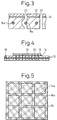
- the mount tape 10 and the wafer 12 inserted midway of the beam-like water jet 50 are cut while leaving a slit 20 having a width generally equal to a diameter of the beam-like water jet 50 as shown in Fig. 3. Since the cutting of the mount tape 10 and the wafer 12 is carried out by a laser beam transmitted through the beam-like water jet 50, the wafer 12 can be cut without receiving a large shearing force as when the rotating blade 104 is used for this purpose, as shown in Fig. 9. Accordingly, the wafer 12 is free from cracks or other damage caused by the shearing force generated during the cutting operation. Also, since heat generated during the cutting by the laser beam is quickly removed by the beam-like water jet 50, the wafer 12 is hardly influenced thereby.
- a slit 20 of a linear shape is formed.
- the laser beam cuts a resin portion softer than the glass filament 18a.
- the glass filament 18a is not cut and is left in the slit 20 as it is.
- the glass cloth 18 is not cut as shown in Fig. 4, whereby the cut pieces of the wafer 12 and the mount tape 10 carrying individual semiconductor elements 13 are maintained in a connected state.
- Fig. 5 shows the arrangement of the slits 20 cutting the wafer 12 into individual semiconductor elements 13 and the glass filaments 18a.
- the orientation of a mesh of the glass filaments 18a and that of the slits 20 do not coincide with each other.
- the glass filament 18a makes an angle in a range from 30 to 60 degrees relative to the slits 20.
- a suitable number of glass filaments 18a in an area of the individual semiconductor 13 is approximately one/mm. Since a total thickness of the mount tape 10 is generally in a range from 80 to 100 ⁇ m, a diameter of the glass filament 18a preferably in a range from 20 to 90 ⁇ m. The diameter of the glass filament is preferably as small as possible provided the strength of the mount tape 10 is maintained even after the cutting.
- the wafer 12 may be cut along a complicated cutting slit, for example, a crank-shaped slit.
- a complicated cutting slit for example, a crank-shaped slit.
- the ultraviolet-curing resin for adhering the semiconductor element 13 is deteriorated by the irradiation with ultraviolet rays.
- liquid for the beam-like liquid jet 50 While pure water is used as liquid for the beam-like liquid jet 50 in the above description, another transparent liquid may be used such as alcohol or others.
- the transparency is not indispensable, however, because it is sufficient that the liquid of the beam-like jet can transmit a laser beam of a specific wavelength.
- the pressure of the beam-like water jet 50 output from the nozzle section 42 is excessively high, there is a risk in that the wafer 12 may be cut by the water jet 50, whereby the pressure is preferably adjusted to a proper level at which the wafer 12 is not cut.
- the output of the laser beam is excessively high, there is a risk in that the mesh-like member such as glass cloth 18 may be cut, whereby the output of the laser beam preferably adjusted to a proper level at which the mesh-like member is not cut.
- a glass cloth is used as a mesh-like member in the above description
- another material such as a metallic cloth composed of metallic fibers or a non-woven cloth composed of glass fibers or metallic fibers, may be used.
- the present invention it is possible to reduce a shearing force applied to a wafer when it is cut and to minimize the adverse effect thereof on the semiconductor element thus cut, whereby the yield of the semiconductor element can be improved.
Landscapes
- Engineering & Computer Science (AREA)
- Physics & Mathematics (AREA)
- Optics & Photonics (AREA)
- Plasma & Fusion (AREA)
- Mechanical Engineering (AREA)
- Dicing (AREA)
- Laser Beam Processing (AREA)
- Processing Of Stones Or Stones Resemblance Materials (AREA)
Abstract
Description
Claims (8)
- A method for cutting a semiconductor wafer, said method comprising the following steps of:adhering a mount tape on a back surface of said semiconductor wafer, said mount tape comprising a resin base and a mesh-like member made of a material harder than that of said resin base and embedded in said resin base; andejecting a beam-like liquid jet toward a front surface of said semiconductor wafer and simultaneously transmitting a laser beam axially through said beam-like liquid jet, so that said semiconductor wafer is cut into individual pieces by said laser beam together with said resin base of the mount tape, while said mesh-like member remains in its connected state.
- A method as set forth in claim 1, wherein said beam-like liquid jet is a pressurized pure water jet and is focused so as to have a diameter in a range of 30 to 50 µm, so that said semiconductor wafer is cut along a slit having a corresponding width.
- A method as set forth in claim 1, wherein said mesh-like member is a glass cloth made of glass filaments.
- A method as set forth in claim 3, wherein said glass cloth comprises a plurality of lateral filaments and a plurality of transverse filaments extending substantially perpendicularly to the lateral filaments, so that said semiconductor wafer is cut along a slit which extends so as not to be in parallel to said lateral and said transverse filaments.
- A method as set forth in claim 4, wherein said semiconductor wafer is cut along a slit which extends at an angle of 30 to 60 degree to said lateral and said transverse filaments.
- A method as set forth in claim 2, wherein a total thickness of said mount tape is in a range from 80 to 100 µm and a diameter of said glass fiber is in a range from 20 to 90 µm.
- A method as set forth in claim 1, wherein a pressure of said beam-like liquid jet and an output of said laser beam is determined in such a manner that said semiconductor wafer is sufficiently cut, while the mesh-like member of the mount tape is not cut, but remains in its connected state.
- An apparatus for cutting a semiconductor wafer comprising:a mount tape comprising a resin base and a mesh-like member made of a material harder than that of said resin base and embedded in said resin base;first means for holding said mount tape, to which a back surface of said the semiconductor wafer is adhered,second means for ejecting a beam-like liquid jet toward a front surface of said semiconductor wafer and simultaneously transmitting a laser beam axially through said beam-like liquid jet;means for moving at least one of said first and second means, so that said semiconductor wafer is cut into individual pieces by said laser beam, together with said resin base of the mount tape, while said mesh-like member remains in its connected state.
Applications Claiming Priority (2)
| Application Number | Priority Date | Filing Date | Title |
|---|---|---|---|
| JP2000136084A JP3484396B2 (en) | 2000-05-09 | 2000-05-09 | Wafer cutting method |
| JP2000136084 | 2000-05-09 |
Publications (3)
| Publication Number | Publication Date |
|---|---|
| EP1153697A2 true EP1153697A2 (en) | 2001-11-14 |
| EP1153697A3 EP1153697A3 (en) | 2003-01-02 |
| EP1153697B1 EP1153697B1 (en) | 2004-03-24 |
Family
ID=18644080
Family Applications (1)
| Application Number | Title | Priority Date | Filing Date |
|---|---|---|---|
| EP01111061A Expired - Lifetime EP1153697B1 (en) | 2000-05-09 | 2001-05-08 | Method and apparatus for cutting a semiconductor wafer |
Country Status (6)
| Country | Link |
|---|---|
| US (1) | US6583383B2 (en) |
| EP (1) | EP1153697B1 (en) |
| JP (1) | JP3484396B2 (en) |
| KR (1) | KR100720050B1 (en) |
| DE (1) | DE60102410T2 (en) |
| TW (1) | TW494538B (en) |
Cited By (1)
| Publication number | Priority date | Publication date | Assignee | Title |
|---|---|---|---|---|
| CN110177766A (en) * | 2017-02-07 | 2019-08-27 | 日本电气硝子株式会社 | Manufacturing method of glass film |
Families Citing this family (30)
| Publication number | Priority date | Publication date | Assignee | Title |
|---|---|---|---|---|
| JP4087144B2 (en) * | 2001-04-23 | 2008-05-21 | 古河電気工業株式会社 | Laser dicing adhesive tape |
| JP2003151924A (en) * | 2001-08-28 | 2003-05-23 | Tokyo Seimitsu Co Ltd | Dicing method and dicing apparatus |
| SG139508A1 (en) * | 2001-09-10 | 2008-02-29 | Micron Technology Inc | Wafer dicing device and method |
| US20030062126A1 (en) * | 2001-10-03 | 2003-04-03 | Scaggs Michael J. | Method and apparatus for assisting laser material processing |
| SG102639A1 (en) | 2001-10-08 | 2004-03-26 | Micron Technology Inc | Apparatus and method for packing circuits |
| JP2003173988A (en) * | 2001-12-04 | 2003-06-20 | Furukawa Electric Co Ltd:The | Semiconductor wafer dicing method |
| SG142115A1 (en) | 2002-06-14 | 2008-05-28 | Micron Technology Inc | Wafer level packaging |
| SG119185A1 (en) | 2003-05-06 | 2006-02-28 | Micron Technology Inc | Method for packaging circuits and packaged circuits |
| EP1662970A2 (en) * | 2003-09-17 | 2006-06-07 | Becton, Dickinson and Company | System and method for creating linear and non-linear trenches in silicon and other crystalline materials with a router |
| US7893386B2 (en) * | 2003-11-14 | 2011-02-22 | Hewlett-Packard Development Company, L.P. | Laser micromachining and methods of same |
| JP2005203541A (en) * | 2004-01-15 | 2005-07-28 | Disco Abrasive Syst Ltd | Wafer laser processing method |
| US6972244B1 (en) * | 2004-04-23 | 2005-12-06 | National Semiconductor Corporation | Marking semiconductor devices through a mount tape |
| US20060027542A1 (en) * | 2004-04-28 | 2006-02-09 | Niraj Mahadev | Method to eliminate defects on the periphery of a slider due to conventional machining processes |
| EP1598140A1 (en) * | 2004-05-19 | 2005-11-23 | Synova S.A. | Laser machining |
| EP1657020A1 (en) * | 2004-11-10 | 2006-05-17 | Synova S.A. | Process and device for optimising the coherence of a fluidjet used for materialworking and fluid flow nozzle for such a device |
| KR100856977B1 (en) * | 2004-11-11 | 2008-09-04 | 야마하 가부시키가이샤 | Semiconductor device, semiconductor wafer, chip size package, and method of manufacturing and inspection therefor |
| JP4997723B2 (en) * | 2005-07-21 | 2012-08-08 | 澁谷工業株式会社 | Hybrid laser processing equipment |
| US20080067159A1 (en) * | 2006-09-19 | 2008-03-20 | General Electric Company | Laser processing system and method for material processing |
| DE102008028213A1 (en) * | 2008-06-06 | 2009-12-10 | Gebr. Schmid Gmbh & Co. | Method for attaching a silicon block to a support therefor and corresponding arrangement |
| JP4645863B2 (en) * | 2008-09-09 | 2011-03-09 | カシオ計算機株式会社 | Manufacturing method of semiconductor device |
| FI125379B (en) * | 2010-10-25 | 2015-09-15 | Jot Automation Oy | Chassis |
| JP6276947B2 (en) * | 2013-09-02 | 2018-02-07 | 株式会社ディスコ | Processing method |
| EP2957378A1 (en) * | 2014-06-16 | 2015-12-23 | Synova SA | Machining head for coupling a laser beam and a fluid beam with an interface |
| CN104368911B (en) * | 2014-10-28 | 2016-12-07 | 中国科学院宁波材料技术与工程研究所 | Laser Machining head and application, laser-processing system and method |
| CN104759753B (en) * | 2015-03-30 | 2016-08-31 | 江苏大学 | The co-ordination of multisystem automatization improves the method for induced with laser cavitation reinforcement |
| US10525554B2 (en) * | 2015-10-30 | 2020-01-07 | Hypertherm, Inc. | Water cooling of laser components |
| JP6965094B2 (en) | 2017-10-17 | 2021-11-10 | 株式会社ディスコ | Laser processing equipment |
| JP6907091B2 (en) | 2017-10-19 | 2021-07-21 | 株式会社ディスコ | Laser processing equipment |
| JP6852031B2 (en) * | 2018-09-26 | 2021-03-31 | 株式会社東芝 | Welding equipment and nozzle equipment |
| DE102019103659B4 (en) * | 2019-02-13 | 2023-11-30 | Bystronic Laser Ag | Gas guide, laser cutting head and laser cutting machine |
Family Cites Families (9)
| Publication number | Priority date | Publication date | Assignee | Title |
|---|---|---|---|---|
| US4239567A (en) | 1978-10-16 | 1980-12-16 | Western Electric Company, Inc. | Removably holding planar articles for polishing operations |
| EP0129603A4 (en) * | 1982-12-17 | 1985-06-10 | Inoue Japax Res | Laser machining apparatus. |
| DE3809921A1 (en) | 1988-03-24 | 1989-10-12 | Diehl Gmbh & Co | Large-area high-energy laser mirror and method for producing such a mirror |
| DE4418845C5 (en) | 1994-05-30 | 2012-01-05 | Synova S.A. | Method and device for material processing using a laser beam |
| US5776220A (en) * | 1994-09-19 | 1998-07-07 | Corning Incorporated | Method and apparatus for breaking brittle materials |
| KR970008386A (en) * | 1995-07-07 | 1997-02-24 | 하라 세이지 | A method of dividing a substrate and a dividing device |
| IT1284082B1 (en) * | 1996-06-27 | 1998-05-08 | Calp Spa | METHOD AND DEVICE FOR CUTTING BY A LASER BEAM OF HOLLOW GLASS ARTICLES |
| JP3593451B2 (en) | 1998-04-01 | 2004-11-24 | 株式会社日平トヤマ | Ingot slicing method |
| ATE424040T1 (en) | 2000-03-30 | 2009-03-15 | Nitto Denko Corp | WATER-PERMEABLE ADHESIVE TAPE FOR PROCESSING SEMICONDUCTORS |
-
2000
- 2000-05-09 JP JP2000136084A patent/JP3484396B2/en not_active Expired - Fee Related
-
2001
- 2001-05-02 US US09/847,193 patent/US6583383B2/en not_active Expired - Fee Related
- 2001-05-04 KR KR1020010024329A patent/KR100720050B1/en not_active Expired - Fee Related
- 2001-05-08 EP EP01111061A patent/EP1153697B1/en not_active Expired - Lifetime
- 2001-05-08 TW TW090110924A patent/TW494538B/en not_active IP Right Cessation
- 2001-05-08 DE DE60102410T patent/DE60102410T2/en not_active Expired - Lifetime
Cited By (2)
| Publication number | Priority date | Publication date | Assignee | Title |
|---|---|---|---|---|
| CN110177766A (en) * | 2017-02-07 | 2019-08-27 | 日本电气硝子株式会社 | Manufacturing method of glass film |
| CN110177766B (en) * | 2017-02-07 | 2021-12-10 | 日本电气硝子株式会社 | Method for producing glass film |
Also Published As
| Publication number | Publication date |
|---|---|
| EP1153697A3 (en) | 2003-01-02 |
| KR100720050B1 (en) | 2007-05-18 |
| JP3484396B2 (en) | 2004-01-06 |
| US6583383B2 (en) | 2003-06-24 |
| DE60102410T2 (en) | 2004-08-19 |
| KR20020017917A (en) | 2002-03-07 |
| JP2001319898A (en) | 2001-11-16 |
| DE60102410D1 (en) | 2004-04-29 |
| TW494538B (en) | 2002-07-11 |
| US20010040152A1 (en) | 2001-11-15 |
| EP1153697B1 (en) | 2004-03-24 |
Similar Documents
| Publication | Publication Date | Title |
|---|---|---|
| EP1153697B1 (en) | Method and apparatus for cutting a semiconductor wafer | |
| KR101432956B1 (en) | Laser processing method | |
| KR101252884B1 (en) | Laser processing method | |
| US8523636B2 (en) | Working object grinding method | |
| US8740474B2 (en) | Methods for processing a multi-fiber ferrule | |
| DE112004000768B4 (en) | Method for separating a plate-like element | |
| DE102021207672B4 (en) | SI substrate production process | |
| EP1293316A1 (en) | Dicing method and apparatus | |
| US20040026382A1 (en) | Method for cutting an object and or futher processing the cut material an carrier for holding the object and the cut material | |
| US20060040472A1 (en) | Method for separating semiconductor substrate | |
| JP2005086111A (en) | Method for cutting semiconductor substrate | |
| DE102013205644A1 (en) | Method for forming chips i.e. semiconductor chips, with adhesive films, involves attaching adhesive film to rear of wafer, and separating wafer from adhesive film to obtain individual chips such that each chip is mounted on rear side film | |
| JP2006173520A (en) | Laser cleaving method and cleaved member that can be cleaved by the method | |
| JP2015115538A (en) | Wafer processing method | |
| DE102013211896B4 (en) | processing method and processing device | |
| JP4697823B2 (en) | Method for dividing brittle substrate | |
| JP3347085B2 (en) | Method of preparing end faces on integrated circuits | |
| JP4288092B2 (en) | Method for manufacturing a chip from a thin wafer | |
| US6517721B1 (en) | Dialyzers and method for modifying the same using a laser | |
| WO2025080124A1 (en) | A method of manufacturing a nozzle assembly, comprising weakening a wafer at at least two focal zones in the depth direction by focusing a laser beam | |
| KR20220063728A (en) | Wafer processing method | |
| WO2021102065A1 (en) | Method of cutting combined structure of glass substrate and light-absorbing plate | |
| JP2003215360A (en) | Optical fiber and processing method thereof | |
| TW200811069A (en) | Processing method of glass lens | |
| KR20070096266A (en) | How to separate individual semiconductor chips |
Legal Events
| Date | Code | Title | Description |
|---|---|---|---|
| PUAI | Public reference made under article 153(3) epc to a published international application that has entered the european phase |
Free format text: ORIGINAL CODE: 0009012 |
|
| AK | Designated contracting states |
Kind code of ref document: A2 Designated state(s): AT BE CH CY DE DK ES FI FR GB GR IE IT LI LU MC NL PT SE TR |
|
| AX | Request for extension of the european patent |
Free format text: AL;LT;LV;MK;RO;SI |
|
| PUAL | Search report despatched |
Free format text: ORIGINAL CODE: 0009013 |
|
| AK | Designated contracting states |
Kind code of ref document: A3 Designated state(s): AT BE CH CY DE DK ES FI FR GB GR IE IT LI LU MC NL PT SE TR |
|
| AX | Request for extension of the european patent |
Free format text: AL;LT;LV;MK;RO;SI |
|
| 17P | Request for examination filed |
Effective date: 20030109 |
|
| GRAP | Despatch of communication of intention to grant a patent |
Free format text: ORIGINAL CODE: EPIDOSNIGR1 |
|
| AKX | Designation fees paid |
Designated state(s): DE |
|
| GRAS | Grant fee paid |
Free format text: ORIGINAL CODE: EPIDOSNIGR3 |
|
| GRAA | (expected) grant |
Free format text: ORIGINAL CODE: 0009210 |
|
| AK | Designated contracting states |
Kind code of ref document: B1 Designated state(s): DE |
|
| RIN1 | Information on inventor provided before grant (corrected) |
Inventor name: SAKAGUCHI, HIDEAKI Inventor name: HIGASHI, MITSUTOSHI |
|
| REG | Reference to a national code |
Ref country code: IE Ref legal event code: FG4D |
|
| REF | Corresponds to: |
Ref document number: 60102410 Country of ref document: DE Date of ref document: 20040429 Kind code of ref document: P |
|
| PLBE | No opposition filed within time limit |
Free format text: ORIGINAL CODE: 0009261 |
|
| STAA | Information on the status of an ep patent application or granted ep patent |
Free format text: STATUS: NO OPPOSITION FILED WITHIN TIME LIMIT |
|
| REG | Reference to a national code |
Ref country code: IE Ref legal event code: MM4A |
|
| 26N | No opposition filed |
Effective date: 20041228 |
|
| PGFP | Annual fee paid to national office [announced via postgrant information from national office to epo] |
Ref country code: DE Payment date: 20130515 Year of fee payment: 13 |
|
| REG | Reference to a national code |
Ref country code: DE Ref legal event code: R119 Ref document number: 60102410 Country of ref document: DE |
|
| REG | Reference to a national code |
Ref country code: DE Ref legal event code: R119 Ref document number: 60102410 Country of ref document: DE Effective date: 20141202 |
|
| PG25 | Lapsed in a contracting state [announced via postgrant information from national office to epo] |
Ref country code: DE Free format text: LAPSE BECAUSE OF NON-PAYMENT OF DUE FEES Effective date: 20141202 |