EP1153476B1 - Circuit de compensation de bruit et d'erreurs a partir d'un etage de sortie d'un amplificateur numerique - Google Patents
Circuit de compensation de bruit et d'erreurs a partir d'un etage de sortie d'un amplificateur numerique Download PDFInfo
- Publication number
- EP1153476B1 EP1153476B1 EP00901496A EP00901496A EP1153476B1 EP 1153476 B1 EP1153476 B1 EP 1153476B1 EP 00901496 A EP00901496 A EP 00901496A EP 00901496 A EP00901496 A EP 00901496A EP 1153476 B1 EP1153476 B1 EP 1153476B1
- Authority
- EP
- European Patent Office
- Prior art keywords
- signal
- digital
- circuit
- feedback path
- amplifier
- Prior art date
- Legal status (The legal status is an assumption and is not a legal conclusion. Google has not performed a legal analysis and makes no representation as to the accuracy of the status listed.)
- Expired - Lifetime
Links
Images


Classifications
-
- H—ELECTRICITY
- H03—ELECTRONIC CIRCUITRY
- H03F—AMPLIFIERS
- H03F3/00—Amplifiers with only discharge tubes or only semiconductor devices as amplifying elements
- H03F3/20—Power amplifiers, e.g. Class B amplifiers, Class C amplifiers
- H03F3/21—Power amplifiers, e.g. Class B amplifiers, Class C amplifiers with semiconductor devices only
- H03F3/217—Class D power amplifiers; Switching amplifiers
- H03F3/2175—Class D power amplifiers; Switching amplifiers using analogue-digital or digital-analogue conversion
-
- H—ELECTRICITY
- H03—ELECTRONIC CIRCUITRY
- H03F—AMPLIFIERS
- H03F1/00—Details of amplifiers with only discharge tubes, only semiconductor devices or only unspecified devices as amplifying elements
- H03F1/30—Modifications of amplifiers to reduce influence of variations of temperature or supply voltage or other physical parameters
-
- H—ELECTRICITY
- H03—ELECTRONIC CIRCUITRY
- H03F—AMPLIFIERS
- H03F2200/00—Indexing scheme relating to amplifiers
- H03F2200/331—Sigma delta modulation being used in an amplifying circuit
Definitions
- the invention relates to a digital amplifier comprising a circuit for compensating errors in the form of noise and/or distortion from the output stage of the digital amplifier, the digital amplifier comprising:
- the invention relates to a method for compensating errors in the form of noise and/or distortion from the output stage of a digital amplifier in which a pulse modulator generates a set of control pulses in response to an input signal transferred to the amplifier and in response to a digital compensation signal, said output stage comprises a first switching output stage for producing the output from the amplifier.
- a known manner, cf. e.g. US Patent No. 5559467, of compensating noise and errors in a digital amplifier comprises feeding the signal of the power supply in a feedforward coupling to an A/D converter which, via a divider circuit dividing an interpolated input signal by the output signal of the A/D converter, is fed to a noise shaper whose output is fed to a pulse width modulator which provides a correction signal that, from the input signals removes ripple voltages from the power supply.
- This known way of eliminating ripple voltages requires relatively expensive non-linear circuit components and/or signal computations. For example, is the division process a time consuming task on a digital signal processor.
- An improved circuit disclosed by the inventor of US Patent No. 5559467 in the publication "IEEE, Power Electronocs Specialist Conf. REC., 1995, p 96 - 102, vol. 1", comprises further a predictor filter to compensate for the delays in the feedforward compensation loop (e.g. delays in the A/D converter and in the digital amplifier).
- the drawback is that the prediction filter is relatively expensive expressed in hardware or comutation cycles of a digital signal processor.
- a prediction filter will normally amplify high frequency noise in the system possibly resulting an adverse effect on the system performance.
- an object of the invention is to provide a circuit which is partly more accurate and is partly less expensive to implement than the mentioned known circuits.
- the compensation circuit comprises:
- the feedback path around the MDAC comprises an analog to digital converting circuit separating a digital section of the feedback path from an analog section of the feedback path.
- the feedback path comprises an analog to digital converting circuit (ADC) adapted to receive an analog signal from the analog section of the feedback path and producing a digital converter output signal feeding into the digital section of the feedback path.
- ADC analog to digital converting circuit
- the compensation circuit is formed by a regulation loop formed by a feedback path around a multiplying D/A converter with an analogue input which receives an error signal, such as a multiplicative error signal m(t) (to be explained below), characteristic of the output stage on its analogue input, said multiplying D/A converter multiplying the multiplicative error signal m(t) by a compensating signal c(k) which is provided in the regulation loop.
- the compensation signal c(k) is fed to a second input of the pulse modulator that produces an output signal in response to the amplifier input signal and the compensation signal in order to compensate for the errors in the output stage. This can e.g. be achieved by comprising a multiplication of the amplifier input signal by the compensation signal.
- the feedback path has a transfer characteristic with a high gain in particular at low frequencies, it is ensured that the errors are compensated in particular well at low frequencies ( e.g. in the audio band).
- the low-pass filter transfer characteristic of the feedback path will compensate the delays that occur in the compensation circuit.
- the low-pass filter characteristic results in a noise shaper effect, which gives the additional advantage that it is sufficient to work with an ADC with lower resolution and precision (e.g. with a much lower number of bits than by linearly coded audio PCM, i.e. typically in the range of 1-10 bits).
- the ADC can be realized as a simple and inexpensive circuit that has a low response delay.
- the analog section of rhe feedback path is adapted to receive a reference input voltage then this reference input voltage can designate the reference point for the compensation circuit, the reference operating state where no compensation is needed.
- the analog to digital converting circuit comprises one or more local feedback path(s)
- such local feedback paths can help to improve the precision of the ADC circuit or, conversely, to relax the needed precision of the components in the ADC circuit. Further, the local feedback paths can improve the overall stability of the regulation loop.
- the analog to digital conversion circuit produces a one-bit (i.e. 1 - bit) digital converter output signal
- the ADC circuit as well as other parts of the compensation circuit may be realized by quite simple and inexpensive circuit components with reduced accuracy and tolerance requirements.
- the invention also relates to a method.
- This method is characterized in that an analog and a digital signal is transferred to the input of a multiplying D/A converter MDAC for delivering at its output an analog signal, said output signal being being transferred in a feedback path to the digital input of the MDAC, said feedback path having a digital and an analog section, said digital section being used for deriving the compensation signal.
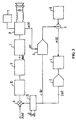
- Fig. 1 shows a known digital amplifier where the numeral 1 designates a UPWM modulator which pulse-width modulates an audio signal that is demodulated (recreated) in a switching output stage (here shown as an H-bridge) and a subsequent low-pass filter. The output from the low-pass filter is connected to the loudspeaker shown in the figure.
- the H-bridge receives voltage from a power supply 7.
- a compensation circuit is inserted with a view to eliminating noise or ripple voltages from the power supply 7 and feeds forward a compensation signal c(k) in the set-up shown, cf. the following.
- An error signal is measured by means of an A/D converter 13 to whose two inputs a reference signal and a signal from the power supply 7 are fed, respectively.
- the ratio between these signals constitutes the multiplicative error which is fed to a predictor 14, whose output signal x is fed to a divider circuit 15 in which the division 1/X is performed to form a compensation signal.
- This circuit contains non-linear circuit components, e.g. the divider circuit 15, and a relatively expensive prediction circuit.
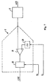
- the invention is based on a more general compensation circuit topology cf. figure 2 receiving a generalized error signal m(t) that is generated in response to signals in the power supply circuit 7 and switching output stage 8.
- the compensation circuit 35 produces then a digital compensation signal c(k) in response to the error signal and the pulse modulator 36 is adapted to receive the compensation signal in response to both the input signal and the compensation signal.
- Fig. 3 shows a digital amplifier, which consists of a pulse modulator 36, in this embodiment comprising a PCM to PWM conversion circuit (in this example comprising a multiplier 11, feed forward correction circuit 10, noise shaper 9 and a Uniform Pulse Width Modulator - UPWM 1).
- the noise shaper 9 produces a noise-shaped output signal with reduced bit resolution (e.g. 5-10 bits).
- the UPWM modulator 1 produces a set of control signals that again controls a set of switches in an switching output stage (shown as a H-bridge 8) being connected to a power supply circuit 7, thereby allowing audio information in the form of electrical energy to be transferred to a load, shown here as a loudspeaker preceded by a low pass filter consisting of two inductors and a capacitor.
- the switches in the H-bridge transfer power directly from a power supply 7 to the load. This means that if distortion is to be obviated, then the power supply must be very accurate, which will normally require relatively expensive components which incorporate large capacitors and inductances or costly active regulation circuits.
- a regulation loop is inserted according to the invention, said regulation loop receiving an error signal in the form of a multiplicative error signal m(t), and emitting a compensation signal c(k) to a pulse modulator , e.g. to a multiplication circuit 11 via a filter 21, cf. the discussion below.
- the actual regulation loop consists of a multiplier, here shown as a multiplying D/A converter 2, which receives the multiplicative error signal m(t) on the analogue input (in some connections called a reference input - not to be confused with the reference voltage 6 in fig. 3), and the digital compensation signal c(k), provided in the loop.
- a multiplier here shown as a multiplying D/A converter 2 which receives the multiplicative error signal m(t) on the analogue input (in some connections called a reference input - not to be confused with the reference voltage 6 in fig. 3), and the digital compensation signal c(k), provided in the loop.
- a first input of a summation unit 3 is coupled to the output of the multiplying D/A converter 2, and the second input of the summation unit is coupled to reference voltage source Vref 6.
- a second error signal e(t) is formed on the output of the summation unit 3, said second error signal being indicative of an instantaneous error in the regulation loop.
- This second error signal e(t) is fed to a loop filter 4 which is a low-pass filter with a high gain in particular at low frequencies.
- the output from the loop filter 4 is fed to an A/D converter, shown as an ADC circuit 5 in fig. 3.
- the output from this ADC circuit is branched in two signal paths, one of which leading to the digital input on the multiplying D/A converter 2, the other signal path leading to an adaptation filter 21, that produces the compensation signal in response to the ADC converter output.
- the adaptation filter can implement a number of processing steps to provide the compensation signal in a desired form. Examples of such processing steps can be low pass filtering to reduce the high frequency noise contents, change of sample rate (e.g. decimation) to allow different sample rates within the pulse modulator and the compensation loop. Further improvements can be obtained by using non-linear processing to improve the precision of the compensation and to reduce the implementation cost of the system. Examples of such processing steps are given below.
- the compensation signal c(k) (i.e. the output of the adaptation filter 21) is fed to the multiplier 11 of the pulse modulator circuit in which a digital audio signal is multiplied by the compensation signal formed in the regulation loop.
- the audio signal is hereby compensated for the multiplicative errors which are expressed by the multiplicative error signal m(t), which thus indicates the error by reproduction of the pulse coding (e.g. PWM coding) of the audio signal in a multiplicative form (in contrast to the more usually employed additive form).
- the multiplicative error signal describes the temporal variation of the "gain" of the switching output stage( H-bridge 8) and is thereby indicative of the noise and the distortion which the output stage applies to the encoded audio signal.
- the multiplicative error signal m(t) may be formed by an approximation, e.g. by using the power supply voltage of the H-bridge as an approximation for m(t).
- the justification for this approximation is that the output voltage of the H-bridge is substantially proportional to the power supply voltage of the H-bridge, i.e. the power supply voltage expresses the gain as function of time for the H-bridge.
- the error signal m(t) can be derived from one or more signals in the power supply circuit in a way so that the error signal is substantially proportional to the power supply voltage and advanced in time by a time offset relative to the power supply voltage.
- the time offset can beneficially be adapted to compensate for the delays in the compensation loop and digital amplifier. Thereby, the effect of the compensation is maximized.
- the timing lead of the error signal can e.g. be realized by having power supply filter prior to the switching output stage and tapping of a signal before the filter used to derive the error signal m(t).
- the power supply filter can e.g. be a traditional low pass filter consisting of a capacitor and an inductor.
- Other improvements can be to use adaptive signal processing to forecast the error of the H-bridge by using other input signals from the power supply circuit, e.g. the mains voltage.
- m(t) may advantageously be formed as a ratio of the pulse modulated great signal (i.e. output signals of the switching output stage) to the pulse modulated small-signal or input control signal(s) for the output stage, cf. the description of the applicants' International Application No. WO 99/45641 which was not publicly available at the priority date of the present application, and which describes the formation of a multiplicative error signal.
- PWM pulse modulated
- m(t) derived corresponding to equation 2 is used for compensation purposes, it is ensured that both noise and ripple on the power supply, but also errors and non-idealities in the H-bridge are compensated, e.g. finite on-resistance and dynamical switching effects.
- the regulation loop forms a compensation signal c(k) which serves to "turn up" the audio signal when m(t) is diminished (e.g. because the voltage of the power supply drops or because of voltage drop due to the on-resistance of the H-bridge switches) and correspondingly to "turn down” when m(t) increases.
- c(k) which serves to "turn up" the audio signal when m(t) is diminished (e.g. because the voltage of the power supply drops or because of voltage drop due to the on-resistance of the H-bridge switches) and correspondingly to "turn down" when m(t) increases.
- the product of c(k) and m(t) is formed on the output of the multiplying DAC 2 which represents the reproduction of the signal c(k) in the amplifier without compensation for errors.
- the H-bridge performs substantially a multiplication between the power supply voltage and the audio signal which has the shape of a PWM signal, i.e. the H-bridge output is substantially the product of the power supply voltage and the encoded audio signal of the digital amplifier.
- the regulation loop seeks to minimize the second error signal e(t).
- the error signal e(t) is the difference between c(k)*m(t) and a reference signal 6.
- the reference signal 6 is typically a precise and constant DC source which expresses the desired effective gain of the H-bridge, i.e., the reference point for the compensation where no compensation is needed. However, nothing prevents the provision of a volume adjustment in the system in the regulation of the reference voltage 6, i.e. the overall system gain (or volume) will be substantially proportional to the reference voltage 6.
- the ADC circuit 5 performs a sampling and quantization of the output of the loop filter 4 to whose input the error signal e(t) is applied.
- Equation 6 C(z) ⁇ Vref/m + q(z)/(1+m*H(z)).
- c(k) is substantially inversely proportional to m(t), and thereby compensation for the multiplicative error is achieved by multiplication by c(k).
- c(k) includes a quantization error which is noise shaped, i.e. spectrally shaped by the loop filter H(z) 4.
- the loop filter is of the low-pass type with a very high great gain at low frequencies, it is ensured that the error is suppressed in the low frequency range (i.e. audible range).
- low-pass filtering 21 of the correction signal c(k) may advantageously be used before it is employed in the multiplier 11.
- non-linear or adaptive filtering may advantageously be introduced in some embodiments, cf. the subsequent description.
- the filter block 21 may also be adapted to change the sample rate of the incoming signal to the desired sample rate of the pulse modulator.
- the compensation loop consists of an MDAC and an ADC embedded in a feedback path consisting of an analog section and a digital section.
- the compensation signal is in general derived from one or more signals inside the digital section of the feedback path.
- the transfer characteristic of the entire feedback path constitutes the equivalent loop filter that, consequently, can be implemented in part as analog processing and in part by digital processing.
- the discrete-time equivalent loop filter (i.e. equivalent digital filter) H(z) for the combined transfer function of the feedback path has been used.
- the feedback path may also include switched capacitor circuits that operate in discrete-time but using continuous amplitude signal representation.
- the reference signal can in general be injected everywhere in the feedback path, i.e., digitally or in analog circuits or as a combination of both.
- the feedback loop must be stable to operate according to the purpose. Therefore, it must be ensured that the poles of (1*m*H(z)) are within the unit circle.
- the equivalent loop filter H(z) must include the entire transfer function through the loop, including delays in all circuit elements in the loop, e.g. the ADC circuit etc.
- the loop filter must thus be designed such that stability can be achieved with a given filter order.
- the equivalent loop filter should preferably be designed such that optimal error suppression is obtained in a desired frequency band (e.g., the audible range). Generally, a better error suppression can be obtained using a higher filter order of the equivalent loop filter.
- sampling frequency can advantageously be higher (e.g. an integer multiple) than the sampling frequency used by the pulse modulator.
- the compensation circuit may advantageously comprise the use of one-bit (1-bit) digital signals sampled at a typically high sample rate.
- the use of 1-bit signals is known form a certain type of data converters (e.g. sigma-delta or delta-sigma converters known from prior art) using noise-shaping to distribute the quantization noise outside the desired frequency band.
- One advantage of 1-bit signal processing is that the analog data converting elements of the ADC and the MDAC is greatly simplified with relaxed requirements for precision and matching. Such circuit elements are in addition very suited for implementation in Very Large Scale Integration (VLSI) circuits using low cost digital process technology. Furthermore, the use of 1-bit data converter elements can take advantages of the inherent very high speed of circuits implemented in VLSI, i.e. to use clock and sampling frequencies in excess of 100MHz.
- VLSI Very Large Scale Integration
- a multiplication between the analogue input m(t) and the digital input is achieved.
- the half-bridge does not need to handle high power and can be implemented cost-effectively in an integrated circuit using e.g. CMOS (Complementary Metal-On-Oxide) switches (i.e. transistors) arranged as an inverter consisting of a P-channel and N-channel switch.
- CMOS Complementary Metal-On-Oxide
- the MDAC can be formed as a switching output stage analogously to the switching output stage of a digital amplifier, however, as stated, the MDAC does not need to handle high power.
- the embodiment in fig. 5 is thus used for a 1-bit signal.
- Fig. 6 shows a second embodiment of the multiplying D/A converter 2 in fig. 3.
- This embodiment may be used when the digital input of the MDAC is an n-bit signal, e.g., originating directly from an n-bit ADC circuit 5.
- a second pulse modulator e.g. uniform pulse width modulator (UPWM) 16
- UPWM uniform pulse width modulator
- the half-bridge alternatively couples the analogue input signal m(t) or zero to the output of the multiplying D/A converter. This results in a desired multiplication between m(t) and the digital input signal of the MDAC.
- the circuit in fig. 6 may be composed of digital building blocks in a very simple manner. In general, other embodiments can be designed using a pulse modulator embedded in the digital section of the feedback loop.
- Fig. 7 shows an embodiment of the ADC circuit 5.
- This circuit consists of an analogue PWM modulator to form a 1-bit signal.
- a comparator 19 compares the input signal with a carrier waveform (e.g. triangle or saw tooth signal) from the generator 20 which can be synchronized with one of the sampling frequencies of the entire amplifier system.
- the output of the comparator is fed to a D flip-flop 18 which samples the comparator signal with a bit-clock signal of the frequency fb.
- the output of the D flip-flop is thereby a 1-bit signal.
- the quantization accuracy is decided by the ratio between the clock frequencies fb and fs, i.e., it is desirable to operate the system with a high bit clock frequency fb.
- FIG. 8 shows an embodiment of a carrier generator 20 which forms part of the circuit 5.
- This generator consists of a capacitor which can be charged by a constant power source. Simultaneously, the capacitor may be discharged quickly (be short-circuited) by means of a contact which is controlled synchronously with the sampling frequency fs, a brief pulse for the contact being formed for each period. The voltage of the capacitor now forms a saw tooth signal.
- a triangular wave can be generated, e.g. by an integrator circuit fed by a square wave (preferably with 50% duty cycle) of the frequency fs. Other waveforms may be appropriate to change the characteristics of the compensation circuit.
- An alternate embodiment for the ADC circuit can be a sigma-delta modulator that produces a pulse density modulated compensation signal c(k).
- An example of an ADC circuit using sigma-delta modulation can be achieved using the circuit of figure 7 where the carrier waveform generator 20 produces a fixed zero signal. In this case, the feedback path through the MDAC will provide a loop filter for the sigma-delta modulator.
- a sigma-delta modulator is a circuit that can convert an analog waveform into a digital signal of the 1-bit type.
- a sigma-delta modulator comprises typically a 1-bit sampling unit (e.g. comparator with a D-flip flop), a D/A converting unit (e.g. analogous to figure 5) and a loop filter structure that applies feedback around the 1-bit sampling unit to suppress quantization noise in a desired frequency band.
- the more general embodiment of the ADC circuit shown in figure 12 shows an example of how a local feedback path can be implemented, in which 31 is a sampling and A/D converting element (e.g. low resolution converter such as a comparator and D-flip flop etc.) receiving a sampling clock signal, 30 is a D/A converter (e.g. a 1-bit D/A converter), 33 is an analog network implementing the local feedback path and possibly receiving a carrier waveform, 32 is digital circuit forming the ADC circuit output signal and providing digital input to the D/A converter 30.
- This general embodiment can implement a variety of noise-shaped and over-sampling ADC converters, including pulse width modulated converters and sigma-delta modulators like the embodiment of figure 7.
- the advantage of having a local feedback path in the ADC circuit is that less gain is needed in the overall feedback path through the MDAC in order to suppress errors of the ADC circuit. Furthermore, the local feedback path can also de adapted to improve the overall stability of the system, since the local feedback path changes the overall equivalent loop transfer characteristic.
- the output of the ADC circuit may advantageously be a 1-bit (or few bit) digital signal sampled at a quite high sample rate, e.g. a bit clock frequency fb that can exceed 100Mhz in frequency using VLSI implementations.
- a bit clock frequency fb that can exceed 100Mhz in frequency using VLSI implementations.
- Such high sample rate is typically not accepted by the pulse modulator and a sample rate change is needed.
- the sample-rate change can be implemented as a decimation process, i.e. a band-limiting filtering followed by a down sampling (i.e. re-sampling to a lower frequency).
- a decimation process i.e. a band-limiting filtering followed by a down sampling (i.e. re-sampling to a lower frequency).
- the art of decimation is well known in the literature and shall not be described further here.
- there are certain implementation aspects for a decimator running at excess of 100MHz on the input i.e. such circuitry is highly costly.
- the band-limiting filter must be very effective such that aliasing errors are avoided by the down sampling.
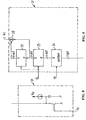
- Figure 9 shows an embodiment of the adaptation filter 21 which receives the 1-bit signal sampled at the bit clock frequency fb and performs down-sampling to the n-bit signal c(k) sampled at the switch frequency fs.
- the embodiment consists of an up/down (or up/hold) counter 24 which is clocked by fb, and which is controlled up or down (up or hold) depending on the incoming 1-bit signal. Synchronously with fs, the output of the counter 24 is sampled by a first latch 23 and whose output is sampled by a second latch 22. Subtraction 25 between the outputs of the two latches 22, 23 gives the compensation output signal c(k).
- the shown circuit of figure 9 computes the pulse width expressed as the integral of the incoming 1-bit signal over each sampling period for the compensation signal.
- This filter is normally referred to as a "sinc" filter.
- Figure 9 thus implements a decimator using a sinc filter running at the high input sample rate fb and down sampling to fs.
- the sinc filter is not a very good band-limiting filter, so aliasing errors occur.
- the circuit of figure 9 is simple to implement and can be operated with very high speed fb in a VLSI circuit.
- circuit of figure 9 acts as a PWM to PCM translator. Since the conversion between PCM and PWM is known to be highly on-linear, errors are to be expected using the circuit of figure 9.
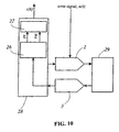
- Figure 10 shows a general structure that can implement such processing, in which the digital section of the feedback path 28 comprises a pulse detector 26 and a further processing circuit 27.
- the pulse detector extracts two signals, the pulse width and the pulse position for each pulse period or sample interval of fs.
- the circuit of figure 9 actually implements the pulse detector that extracts the pulse width, but not the pulse position.
- the pulse position can be extracted using a counter and detector circuit that detects the rising and falling transition of the incoming 1-bit signal.
- the middle point between these two timing instants e.g. read-out from the counter at the transition instants
- the difference of the transition point time instants expresses the pulse width. Consequently, a counter/detector circuit can implement the pulse detector 26 in figure 10.
- the pulse position signal carriers further information together with the pulse width signal, needed to construct a high precision compensation signal output. Note that the pulse position information is disregarded in the circuit of figure 9, i.e., a lower precision is accomplished than by using the pulse position information.
- a processing circuit of figure 11 uses a multiplier to form the product of the pulse width PW and the pulse position PP, the product being fed to a filter with a transfer function substantially equal to j ⁇ followed by a scaling by a constant and summation with the pulse width signal PW.
- the resulting signal will then have a much higher precision than by just using the pulse width.
- the advantage of the non-linear processing is that it is performed at a low sample rate as opposed to the possibly very high fb clock rate.
- the circuit of figure 11 can be implemented simply in VLSI with very low circuit complexity and processing delays.
- the pulse detector can still operate with a very high fb clock frequency to maximize the resolution of the compensation signal.
Landscapes
- Engineering & Computer Science (AREA)
- Power Engineering (AREA)
- Amplifiers (AREA)
- Compression, Expansion, Code Conversion, And Decoders (AREA)
Claims (19)
- Amplificateur numérique comprenant un circuit de compensation d'erreurs sous la forme de bruit et/ou de distorsion provenant de l'étage de sortie de l'amplificateur numérique, l'amplificateur numérique comprenant :caractérisé en ce que le circuit de compensation comprend :un modulateur (36) d'impulsions conçu pour produire un ensemble d'impulsions de commande en réponse au signal d'entrée de l'amplificateur numérique et en réponse à un signal numérique (c(k)) de compensation,un premier étage (8) de sortie à commutation relié à un circuit (7) d'alimentation en puissance, le premier étage de sortie à commutation étant conçu pour recevoir l'ensemble d'impulsions de commande et produire la sortie de convertisseur d'amplificateur numérique,un convertisseur multiplieur numérique-analogique (MDAC) (2) recevant un signal analogique (m(t)) d'entrée et un signal numérique (c(k)) d'entrée, et produisant un signal analogique de sortie,l'entrée analogique (m(t)) du convertisseur multiplieur numérique-analogique recevant un signal d'erreur caractéristique d'erreurs et/ou de bruit dans l'étage de sortie,un trajet (3, 4, 5, 28, 29) de rétroaction de la sortie analogique du convertisseur multiplieur numérique-analogique (2) à l'entrée numérique dudit convertisseur (2),le trajet de rétroaction ayant une section numérique-et une section analogique (3, 4, 29),le signal numérique (c(k)) de compensation étant extrait d'un ou plusieurs signaux dans la section numérique (5, 28) du trajet (3, 4, 5, 28, 29) de rétroaction.
- Amplificateur selon la revendication 1, caractérisé en ce que le trajet (3, 4, 5, 28, 29) de rétroaction comprend un circuit convertisseur analogique-numérique (ÀDC) (5) conçu pour recevoir un signal analogique de la section analogique (3, 4, 29) du trajet (3, 4, 5) de rétroaction et produisant un signal numérique de sortie de convertisseur envoyé à la section numérique (5, 28) du trajet (3, 4, 5, 28, 29) de rétroaction.
- Amplificateur selon la revendication 2, caractérisé en ce que le trajet (3, 4, 5, 28, 29) de rétroaction a une caractéristique de transfert avec un gain élevé, en particulier aux fréquences basses.
- Amplificateur selon la revendication 3, caractérisé en ce que la section analogique (3, 4, 29) du trajet (3, 4, 5, 28, 29) de rétroaction est conçue pour recevoir une tension (6) d'entrée de référence.
- Amplificateur selon la revendication 4, caractérisé en ce que le convertisseur analogique-numérique (ADC) (5) comprend un ou plusieurs trajets locaux (30, 31, 32) de rétroaction.
- Amplificateur selon l'une quelconque des revendications 2 à 5, caractérisé en ce que le convertisseur analogique-numérique (ADC) (5) produit un signal numérique (fig. 7) d'un bit (c'est-à-dire bit 1) de sortie de convertisseur.
- Amplificateur selon l'une quelconque des revendications 1 à 6, caractérisé en ce que le convertisseur analogique-numérique (ADC) (5) comprend un modulateur (fig. 7) de largeur d'impulsions ou un modulateur sigma-delta.
- Amplificateur selon l'une quelconque des revendications 1 à 7, caractérisé en ce que la section numérique (5, 28) du trajet (3, 4, 5, 28, 29) de rétroaction comprend un modulateur (16) d'impulsions.
- Amplificateur selon l'une quelconque des revendications 1 à 8; caractérisé en ce que le convertisseur multiplieur numérique-analogique (MDAC) (2) est formé par un deuxième étage de sortie (fig. 5, 6) à commutation recevant un signal d'erreur et étant commandé par un ou plusieurs signaux numériques (c(k)) provenant de la section numérique (5, 28) du trajet (3, 4, 5, 28, 29) de rétroaction.
- Amplificateur selon la revendication 9, caractérisé en ce que le deuxième étage de sortie (fig. 5, 6) à commutation est formé par un demi-pont (17).
- Amplificateur selon l'une quelconque des revendications 2 à 10, caractérisé en ce que le signal numérique (c(k)) de compensation est extrait du signal (c(k)) de sortie de convertisseur analogique-numérique (ADC)en utilisant un traitement d'adaptation comprenant (21, fig. 9) un filtrage linéaire et/ou un filtrage non linéaire et/ou une modification de cadence d'échantillonnage.
- Amplificateur selon la revendication 11, caractérisé en ce que le traitement d'adaptation comprend un détecteur (26) d'impulsions conçu pour détecter la largeur (PW) d'impulsion et la position (PP) d'impulsion pour chaque période d'impulsion du signal de sortie de convertisseuranalogique-numérique (ADC), la largeur (PW) et la position (PP) d'impulsion étant traitées pour produire le signal numérique (c(k)) de compensation.
- Amplificateur selon l'une des revendications 1 à 12, caractérisé en ce que le signal numérique (c(k)) de compensation est extrait en utilisant un processus de décimation (fig. 9).
- Amplificateur selon la revendication 13, caractérisé en ce que le processus de décimation comprend un filtre passe-bas synchrone (fig. 9) mis en oeuvre comme un circuit (24) de compteur relié à un circuit (22, 23, 25) de sous-échantillonnage.
- Amplificateur selon l'une des revendications 1 à 14, caractérisé en ce que le circuit de compensation est formé en totalité ou en partie par un circuit intégré.
- Amplificateur selon l'une quelconque des revendications 1 à 15, caractérisé en ce que le signal d'erreur (m(t)) est extrait en utilisant le produit du signal de commande de modulation d'impulsion et le signal de sortie du premier étage de sortie à commutation 8.
- Amplificateur selon l'une quelconque des revendications 1 à 15, caractérisé en ce que le signal d'erreur (m(t)) est extrait du circuit d'alimentation en puissance (7) du premier étage de sortie à commutation de pont - H (8).
- Amplificateur selon l'une quelconque des revendications 1 à 15, caractérisé en ce que le signal d'erreur (m(t)) est adapté pour entraíner la tension d'alimentation en puissance (7) pour le premier étage de sortie à commutation (8) par un décalage de temps.
- Procédé pour compenser des erreurs sous la forme de bruit et/ou de distorsion provenant de l'étage de sortie (8) d'un amplificateur numérique dans lequel un modulateur d'impulsions (86) génère un ensemble d'impulsions de commande en réponse à un signal d'entrée transféré à l'amplificateur en réponse à un signal numérique (c(k)) de compensation, ledit étage de sortie (8) comprenant un premier étage de sortie à commutation (8) pour produire la sortie de l'amplificateur, caractérisé en ce que un signal analogique (m(t)) et un signal numérique (c(k)) sont transférés à l'entrée d'un convertisseur multiplieur numérique analogique (MDCA) (2) pouvant délivrer à sa sortie un signal analogique, ledit signal de sortie étant transféré dans un trajet de rétroaction (3, 4, 5, 28, 29) vers l'entrée numérique du convertisseur multiplieur numérique analogique (MDAC), ledit trajet de rétroaction (3, 4, 5, 28, 29) ayant une section numérique et une section numérique (5, 28) et une section analogique (3,4,29), ladite section numérique étant utilisée pour extraire le signal de compensation (c(k)).
Applications Claiming Priority (3)
| Application Number | Priority Date | Filing Date | Title |
|---|---|---|---|
| DK99001 | 1999-02-03 | ||
| DKPA199900159 | 1999-02-05 | ||
| PCT/DK2000/000048 WO2000046919A2 (fr) | 1999-02-05 | 2000-02-07 | Circuit de compensation de bruit et d'erreurs a partir d'un etage de sortie d'un amplificateur numerique |
Publications (2)
| Publication Number | Publication Date |
|---|---|
| EP1153476A1 EP1153476A1 (fr) | 2001-11-14 |
| EP1153476B1 true EP1153476B1 (fr) | 2003-01-08 |
Family
ID=8090433
Family Applications (1)
| Application Number | Title | Priority Date | Filing Date |
|---|---|---|---|
| EP00901496A Expired - Lifetime EP1153476B1 (fr) | 1999-02-05 | 2000-02-07 | Circuit de compensation de bruit et d'erreurs a partir d'un etage de sortie d'un amplificateur numerique |
Country Status (8)
| Country | Link |
|---|---|
| US (1) | US6518838B1 (fr) |
| EP (1) | EP1153476B1 (fr) |
| JP (1) | JP2002536903A (fr) |
| AT (1) | ATE230900T1 (fr) |
| AU (1) | AU2279600A (fr) |
| DE (1) | DE60001148T2 (fr) |
| DK (1) | DK1153476T3 (fr) |
| WO (1) | WO2000046919A2 (fr) |
Families Citing this family (39)
| Publication number | Priority date | Publication date | Assignee | Title |
|---|---|---|---|---|
| US7173550B1 (en) * | 2001-07-13 | 2007-02-06 | Cirrus Logic, Inc. | Circuits, systems and methods for volume control in low noise 1-bit digital audio systems |
| US6917241B2 (en) * | 2002-05-13 | 2005-07-12 | Matsushita Electric Industrial Co., Ltd. | Amplifier circuit, transmission device, amplification method, and transmission method |
| US6765436B1 (en) * | 2002-09-04 | 2004-07-20 | Cirrus Logic, Inc. | Power supply based audio compression for digital audio amplifier |
| AU2003272025A1 (en) * | 2002-11-22 | 2004-06-18 | Koninklijke Philips Electronics N.V. | Pulse width-modulated noise shaper |
| DE10255352B3 (de) * | 2002-11-27 | 2004-02-12 | Infineon Technologies Ag | Verfahren und Vorrichtung zur Korrektur von Signalverzerrungen in einer Verstärkereinrichtung |
| DE10393487B3 (de) * | 2002-11-27 | 2007-05-16 | Infineon Technologies Ag | Verfahren und Vorrichtung zur Korrektur von Signalverzerrungen in einer Verstärkereinrichtung |
| DE10337782B4 (de) * | 2003-07-14 | 2007-03-01 | Micronas Gmbh | Methode und Schaltung zur effektiven Konvertierung von PCM-in PWM-Daten |
| JP4148077B2 (ja) | 2003-09-10 | 2008-09-10 | 沖電気工業株式会社 | D級信号増幅回路 |
| AU2003304647A1 (en) * | 2003-10-10 | 2005-04-27 | Tc Electronic A/S | Power supply compensation |
| JP4561459B2 (ja) * | 2004-04-30 | 2010-10-13 | ヤマハ株式会社 | D級増幅器 |
| FR2879754A1 (fr) * | 2004-12-20 | 2006-06-23 | St Microelectronics Sa | Transpondeur electromagnetique depourvu d'alimentation autonome |
| JP4802765B2 (ja) * | 2005-03-18 | 2011-10-26 | ヤマハ株式会社 | D級増幅器 |
| US7474149B2 (en) * | 2005-03-25 | 2009-01-06 | Pulsewave Rf, Inc. | Radio frequency power amplifier and method using a controlled supply |
| US7352237B2 (en) * | 2005-03-25 | 2008-04-01 | Pulsewave Rf, Inc. | Radio frequency power amplifier and corresponding method |
| EP1883992A2 (fr) * | 2005-04-28 | 2008-02-06 | Pulsewave RF, Inc. | Amplificateur de puissance radiofrequence et procede utilisant une pluralite de systemes asservis |
| EP1922805A1 (fr) * | 2005-09-01 | 2008-05-21 | Danmarks Tekniske Universitet | Modulateur auto oscillant |
| US7298204B2 (en) * | 2005-11-30 | 2007-11-20 | Pulsus Technologies | Method and apparatus for outputting audio signal |
| EP1964679B1 (fr) | 2005-12-22 | 2011-09-07 | Seiko Epson Corporation | Dispositif de commande d'une tête d imprimante à jet d encre, procédé de commande, et imprimante à jet d encre |
| WO2007083669A1 (fr) | 2006-01-17 | 2007-07-26 | Seiko Epson Corporation | Dispositif d’entraînement de tête d’imprimante à jet d’encre et imprimante à jet d’encre |
| CN101370664B (zh) | 2006-01-20 | 2010-06-02 | 精工爱普生株式会社 | 喷墨打印机的头驱动装置及喷墨打印机 |
| US7436255B2 (en) * | 2006-02-07 | 2008-10-14 | D2Audio Corporation | Power supply feed forward analog input filter component mismatch correction |
| US7822800B2 (en) * | 2006-05-19 | 2010-10-26 | Camco Produktions-Und Vertriebs Gmbh Fur Beschallungs-Und Beleuchtungsanlagen | Apparatus and method for performing a calculation operation |
| JP4946685B2 (ja) | 2006-07-24 | 2012-06-06 | セイコーエプソン株式会社 | 液体噴射装置および印刷装置 |
| JP5141117B2 (ja) | 2006-07-24 | 2013-02-13 | セイコーエプソン株式会社 | 液体噴射装置および印刷装置 |
| US7492219B1 (en) | 2006-08-10 | 2009-02-17 | Marvell International Ltd. | Power efficient amplifier |
| US7724161B1 (en) | 2006-12-12 | 2010-05-25 | Marvell International Ltd. | Truncation for three-level digital amplifier |
| US7731317B2 (en) | 2007-01-12 | 2010-06-08 | Seiko Epson Corporation | Liquid jetting device |
| JP4513832B2 (ja) * | 2007-07-13 | 2010-07-28 | ヤマハ株式会社 | D級増幅回路 |
| JP5256768B2 (ja) | 2008-02-21 | 2013-08-07 | セイコーエプソン株式会社 | 液体噴射装置 |
| JP2012015650A (ja) * | 2010-06-29 | 2012-01-19 | Renesas Electronics Corp | D級増幅器 |
| US9048791B2 (en) * | 2012-04-13 | 2015-06-02 | Taiwan Semiconductor Manufacturing Co., Ltd. | Multi-stage amplifier with pulse width modulation (PWM) noise shaping |
| US9379777B2 (en) * | 2012-05-07 | 2016-06-28 | Nokia Technologies Oy | Near field communication circuitry used for hearing aid compatibility |
| GB2502122B (en) * | 2012-05-17 | 2014-04-23 | Red Lion 49 Ltd | Amplifier |
| US9225253B2 (en) * | 2012-10-23 | 2015-12-29 | Microchip Technology Inc. | High voltage switching linear amplifier and method therefor |
| US9918172B1 (en) | 2016-08-19 | 2018-03-13 | Semiconductor Components Industries, Llc | Active output driver supply compensation for noise reduction |
| US10164576B2 (en) | 2017-04-28 | 2018-12-25 | Cirrus Logic, Inc. | Amplifier offset cancellation using amplifier supply voltage |
| US10938353B2 (en) | 2019-03-26 | 2021-03-02 | Analog Devices International Unlimited Company | Coulomb counter with offset calibration |
| US11563442B2 (en) * | 2020-08-07 | 2023-01-24 | Analog Devices International Unlimited Company | Calibration of continuous-time residue generation systems for analog-to-digital converters |
| CN113300680B (zh) * | 2021-04-09 | 2023-09-15 | 汇顶科技私人有限公司 | 脉冲宽度调变放大器、相关芯片及信号宽度调变的方法 |
Family Cites Families (10)
| Publication number | Priority date | Publication date | Assignee | Title |
|---|---|---|---|---|
| US4495470A (en) | 1983-02-07 | 1985-01-22 | Tektronix, Inc. | Offset balancing method and apparatus for a DC amplifier |
| JPS6139708A (ja) | 1984-07-31 | 1986-02-25 | Akai Electric Co Ltd | パルス幅変調アンプにおける電源電圧変動補正方法 |
| DE3605561A1 (de) | 1986-02-21 | 1987-08-27 | Thomson Brandt Gmbh | Verfahren zur kompensation der offset-spannung eines regelverstaerkers und schaltungsanordnung zur durchfuehrung des verfahrens |
| JP3166321B2 (ja) | 1992-07-01 | 2001-05-14 | 日本電気株式会社 | 変調信号送信システム |
| JP2883260B2 (ja) | 1993-04-20 | 1999-04-19 | 三菱電機株式会社 | 歪補償回路 |
| US5559467A (en) | 1995-01-27 | 1996-09-24 | The Regents Of The University Of California | Digital, pulse width modulation audio power amplifier with noise and ripple shaping |
| DK28398A (da) | 1998-03-03 | 1999-09-04 | Toccata Technology Aps | Fremgangsmåde ved kompensering af ulineariteter i en forstærker, en forstærker, samt anvendelser af fremgangsmåden og forst |
| US6054896A (en) * | 1998-12-17 | 2000-04-25 | Datum Telegraphic Inc. | Controller and associated methods for a linc linear power amplifier |
| US6414614B1 (en) * | 1999-02-23 | 2002-07-02 | Cirrus Logic, Inc. | Power output stage compensation for digital output amplifiers |
| US6373334B1 (en) * | 2000-06-12 | 2002-04-16 | Cirrus Logic, Inc. | Real time correction of a digital PWM amplifier |
-
2000
- 2000-02-07 JP JP2000597893A patent/JP2002536903A/ja active Pending
- 2000-02-07 WO PCT/DK2000/000048 patent/WO2000046919A2/fr active IP Right Grant
- 2000-02-07 DE DE60001148T patent/DE60001148T2/de not_active Expired - Lifetime
- 2000-02-07 AU AU22796/00A patent/AU2279600A/en not_active Abandoned
- 2000-02-07 US US09/890,757 patent/US6518838B1/en not_active Expired - Lifetime
- 2000-02-07 DK DK00901496T patent/DK1153476T3/da active
- 2000-02-07 AT AT00901496T patent/ATE230900T1/de not_active IP Right Cessation
- 2000-02-07 EP EP00901496A patent/EP1153476B1/fr not_active Expired - Lifetime
Also Published As
| Publication number | Publication date |
|---|---|
| WO2000046919A3 (fr) | 2001-02-08 |
| AU2279600A (en) | 2000-08-25 |
| US6518838B1 (en) | 2003-02-11 |
| DE60001148D1 (de) | 2003-02-13 |
| ATE230900T1 (de) | 2003-01-15 |
| DE60001148T2 (de) | 2003-10-23 |
| EP1153476A1 (fr) | 2001-11-14 |
| JP2002536903A (ja) | 2002-10-29 |
| DK1153476T3 (da) | 2003-05-05 |
| WO2000046919A2 (fr) | 2000-08-10 |
Similar Documents
| Publication | Publication Date | Title |
|---|---|---|
| EP1153476B1 (fr) | Circuit de compensation de bruit et d'erreurs a partir d'un etage de sortie d'un amplificateur numerique | |
| Berkhout et al. | Class-D audio amplifiers in mobile applications | |
| US7411448B2 (en) | Class-D amplifier | |
| US7696913B2 (en) | Signal processing system using delta-sigma modulation having an internal stabilizer path with direct output-to-integrator connection | |
| EP0932932B1 (fr) | Dispositif d'amplification de signaux numeriques | |
| AU721526B2 (en) | Conversion of a PCM signal into a UPWM signal | |
| US7276963B2 (en) | Switching power amplifier and method for amplifying a digital input signal | |
| JP5510464B2 (ja) | 独立した遅延を有する複数のフィードバック経路を有する連続時間型シグマデルタ変調器 | |
| EP0906659A1 (fr) | Circuit de traitement des signaux de type mixte a surechantillon nage et mise en forme du bruit | |
| JP2011507425A (ja) | フィードバックパスにおいてビット数の減少したマルチビットシグマ・デルタ変調器 | |
| WO1998011668A1 (fr) | Numeriseur a plage dynamique large | |
| JP2006507743A (ja) | パルス幅変調型ノイズシェーパ | |
| US9362888B2 (en) | Devices and methods for converting digital signals | |
| US7557744B2 (en) | PWM driver and class D amplifier using same | |
| JPH11512274A (ja) | 低電力デルタ・シグマ変換器 | |
| US8698662B2 (en) | System and method for a high resolution digital input class D amplifier with feedback | |
| US8773297B2 (en) | System and method for pulse width modulation digital-to-analog converter | |
| EP1556953B1 (fr) | Convertisseur de donnees | |
| US12015426B2 (en) | System and method of reducing delta-sigma modulator error using force-and-correction | |
| Kulka | Application of pulse modulation techniques for class-D audio power amplifiers | |
| Trehan et al. | A high performance class-D power amplifier using error feedback architecture | |
| EP2157700B1 (fr) | Circuit de convertisseur analogique-numérique delta-sigma et procédé de conversion analogique-numérique | |
| Yu et al. | An FPGA-based digital class-D amplifier with power supply error correction | |
| JPH08167848A (ja) | Δς変換装置の直流電圧補償回路 | |
| KULKA | Acoustic energy distribution in space around the pipe outlet |
Legal Events
| Date | Code | Title | Description |
|---|---|---|---|
| PUAI | Public reference made under article 153(3) epc to a published international application that has entered the european phase |
Free format text: ORIGINAL CODE: 0009012 |
|
| 17P | Request for examination filed |
Effective date: 20010905 |
|
| AK | Designated contracting states |
Kind code of ref document: A1 Designated state(s): AT BE CH CY DE DK ES FI FR GB GR IE IT LI LU MC NL PT SE |
|
| GRAG | Despatch of communication of intention to grant |
Free format text: ORIGINAL CODE: EPIDOS AGRA |
|
| 17Q | First examination report despatched |
Effective date: 20020131 |
|
| GRAG | Despatch of communication of intention to grant |
Free format text: ORIGINAL CODE: EPIDOS AGRA |
|
| GRAG | Despatch of communication of intention to grant |
Free format text: ORIGINAL CODE: EPIDOS AGRA |
|
| GRAH | Despatch of communication of intention to grant a patent |
Free format text: ORIGINAL CODE: EPIDOS IGRA |
|
| GRAH | Despatch of communication of intention to grant a patent |
Free format text: ORIGINAL CODE: EPIDOS IGRA |
|
| GRAA | (expected) grant |
Free format text: ORIGINAL CODE: 0009210 |
|
| RAP1 | Party data changed (applicant data changed or rights of an application transferred) |
Owner name: TEXAS INSTRUMENTS DENMARK A/S |
|
| AK | Designated contracting states |
Kind code of ref document: B1 Designated state(s): AT BE CH CY DE DK ES FI FR GB GR IE IT LI LU MC NL PT SE |
|
| PG25 | Lapsed in a contracting state [announced via postgrant information from national office to epo] |
Ref country code: IT Free format text: LAPSE BECAUSE OF FAILURE TO SUBMIT A TRANSLATION OF THE DESCRIPTION OR TO PAY THE FEE WITHIN THE PRESCRIBED TIME-LIMIT;WARNING: LAPSES OF ITALIAN PATENTS WITH EFFECTIVE DATE BEFORE 2007 MAY HAVE OCCURRED AT ANY TIME BEFORE 2007. THE CORRECT EFFECTIVE DATE MAY BE DIFFERENT FROM THE ONE RECORDED. Effective date: 20030108 Ref country code: BE Free format text: LAPSE BECAUSE OF FAILURE TO SUBMIT A TRANSLATION OF THE DESCRIPTION OR TO PAY THE FEE WITHIN THE PRESCRIBED TIME-LIMIT Effective date: 20030108 Ref country code: LI Free format text: LAPSE BECAUSE OF FAILURE TO SUBMIT A TRANSLATION OF THE DESCRIPTION OR TO PAY THE FEE WITHIN THE PRESCRIBED TIME-LIMIT Effective date: 20030108 Ref country code: FI Free format text: LAPSE BECAUSE OF FAILURE TO SUBMIT A TRANSLATION OF THE DESCRIPTION OR TO PAY THE FEE WITHIN THE PRESCRIBED TIME-LIMIT Effective date: 20030108 Ref country code: AT Free format text: LAPSE BECAUSE OF FAILURE TO SUBMIT A TRANSLATION OF THE DESCRIPTION OR TO PAY THE FEE WITHIN THE PRESCRIBED TIME-LIMIT Effective date: 20030108 Ref country code: GR Free format text: LAPSE BECAUSE OF FAILURE TO SUBMIT A TRANSLATION OF THE DESCRIPTION OR TO PAY THE FEE WITHIN THE PRESCRIBED TIME-LIMIT Effective date: 20030108 Ref country code: CH Free format text: LAPSE BECAUSE OF FAILURE TO SUBMIT A TRANSLATION OF THE DESCRIPTION OR TO PAY THE FEE WITHIN THE PRESCRIBED TIME-LIMIT Effective date: 20030108 Ref country code: NL Free format text: LAPSE BECAUSE OF FAILURE TO SUBMIT A TRANSLATION OF THE DESCRIPTION OR TO PAY THE FEE WITHIN THE PRESCRIBED TIME-LIMIT Effective date: 20030108 |
|
| REF | Corresponds to: |
Ref document number: 230900 Country of ref document: AT Date of ref document: 20030115 Kind code of ref document: T |
|
| REG | Reference to a national code |
Ref country code: GB Ref legal event code: FG4D |
|
| REG | Reference to a national code |
Ref country code: CH Ref legal event code: EP |
|
| REG | Reference to a national code |
Ref country code: IE Ref legal event code: FG4D |
|
| PG25 | Lapsed in a contracting state [announced via postgrant information from national office to epo] |
Ref country code: LU Free format text: LAPSE BECAUSE OF NON-PAYMENT OF DUE FEES Effective date: 20030207 Ref country code: CY Free format text: LAPSE BECAUSE OF FAILURE TO SUBMIT A TRANSLATION OF THE DESCRIPTION OR TO PAY THE FEE WITHIN THE PRESCRIBED TIME-LIMIT Effective date: 20030207 Ref country code: IE Free format text: LAPSE BECAUSE OF NON-PAYMENT OF DUE FEES Effective date: 20030207 |
|
| REF | Corresponds to: |
Ref document number: 60001148 Country of ref document: DE Date of ref document: 20030213 Kind code of ref document: P |
|
| PG25 | Lapsed in a contracting state [announced via postgrant information from national office to epo] |
Ref country code: MC Free format text: LAPSE BECAUSE OF NON-PAYMENT OF DUE FEES Effective date: 20030228 |
|
| PG25 | Lapsed in a contracting state [announced via postgrant information from national office to epo] |
Ref country code: SE Free format text: LAPSE BECAUSE OF FAILURE TO SUBMIT A TRANSLATION OF THE DESCRIPTION OR TO PAY THE FEE WITHIN THE PRESCRIBED TIME-LIMIT Effective date: 20030408 |
|
| PG25 | Lapsed in a contracting state [announced via postgrant information from national office to epo] |
Ref country code: PT Free format text: LAPSE BECAUSE OF FAILURE TO SUBMIT A TRANSLATION OF THE DESCRIPTION OR TO PAY THE FEE WITHIN THE PRESCRIBED TIME-LIMIT Effective date: 20030410 |
|
| REG | Reference to a national code |
Ref country code: DK Ref legal event code: T3 |
|
| REG | Reference to a national code |
Ref country code: CH Ref legal event code: PL |
|
| PG25 | Lapsed in a contracting state [announced via postgrant information from national office to epo] |
Ref country code: ES Free format text: LAPSE BECAUSE OF FAILURE TO SUBMIT A TRANSLATION OF THE DESCRIPTION OR TO PAY THE FEE WITHIN THE PRESCRIBED TIME-LIMIT Effective date: 20030730 |
|
| ET | Fr: translation filed | ||
| PLBE | No opposition filed within time limit |
Free format text: ORIGINAL CODE: 0009261 |
|
| STAA | Information on the status of an ep patent application or granted ep patent |
Free format text: STATUS: NO OPPOSITION FILED WITHIN TIME LIMIT |
|
| REG | Reference to a national code |
Ref country code: IE Ref legal event code: MM4A |
|
| 26N | No opposition filed |
Effective date: 20031009 |
|
| REG | Reference to a national code |
Ref country code: FR Ref legal event code: PLFP Year of fee payment: 16 |
|
| PGFP | Annual fee paid to national office [announced via postgrant information from national office to epo] |
Ref country code: DE Payment date: 20150227 Year of fee payment: 16 Ref country code: DK Payment date: 20150126 Year of fee payment: 16 |
|
| PGFP | Annual fee paid to national office [announced via postgrant information from national office to epo] |
Ref country code: GB Payment date: 20150126 Year of fee payment: 16 Ref country code: FR Payment date: 20150126 Year of fee payment: 16 |
|
| REG | Reference to a national code |
Ref country code: DE Ref legal event code: R119 Ref document number: 60001148 Country of ref document: DE |
|
| REG | Reference to a national code |
Ref country code: DK Ref legal event code: EBP Effective date: 20160229 |
|
| GBPC | Gb: european patent ceased through non-payment of renewal fee |
Effective date: 20160207 |
|
| REG | Reference to a national code |
Ref country code: FR Ref legal event code: ST Effective date: 20161028 |
|
| PG25 | Lapsed in a contracting state [announced via postgrant information from national office to epo] |
Ref country code: GB Free format text: LAPSE BECAUSE OF NON-PAYMENT OF DUE FEES Effective date: 20160207 Ref country code: DE Free format text: LAPSE BECAUSE OF NON-PAYMENT OF DUE FEES Effective date: 20160901 Ref country code: DK Free format text: LAPSE BECAUSE OF NON-PAYMENT OF DUE FEES Effective date: 20160229 Ref country code: FR Free format text: LAPSE BECAUSE OF NON-PAYMENT OF DUE FEES Effective date: 20160229 |