EP1152644A1 - Reduced voltage and time delay to eliminate filament hot shock - Google Patents
Reduced voltage and time delay to eliminate filament hot shock Download PDFInfo
- Publication number
- EP1152644A1 EP1152644A1 EP01304103A EP01304103A EP1152644A1 EP 1152644 A1 EP1152644 A1 EP 1152644A1 EP 01304103 A EP01304103 A EP 01304103A EP 01304103 A EP01304103 A EP 01304103A EP 1152644 A1 EP1152644 A1 EP 1152644A1
- Authority
- EP
- European Patent Office
- Prior art keywords
- lamp
- circuit
- time
- filament
- voltage
- Prior art date
- Legal status (The legal status is an assumption and is not a legal conclusion. Google has not performed a legal analysis and makes no representation as to the accuracy of the status listed.)
- Withdrawn
Links
- 230000035939 shock Effects 0.000 title claims abstract description 21
- 238000009434 installation Methods 0.000 claims abstract description 11
- 238000000034 method Methods 0.000 claims abstract description 8
- 230000003213 activating effect Effects 0.000 claims 1
- 229910052736 halogen Inorganic materials 0.000 abstract description 9
- 150000002367 halogens Chemical class 0.000 abstract description 9
- 239000003990 capacitor Substances 0.000 description 22
- IJGRMHOSHXDMSA-UHFFFAOYSA-N Atomic nitrogen Chemical compound N#N IJGRMHOSHXDMSA-UHFFFAOYSA-N 0.000 description 6
- 229910052757 nitrogen Inorganic materials 0.000 description 3
- 238000013461 design Methods 0.000 description 2
- 238000005286 illumination Methods 0.000 description 2
- 230000005855 radiation Effects 0.000 description 2
- 230000006978 adaptation Effects 0.000 description 1
- 238000013459 approach Methods 0.000 description 1
- 230000015556 catabolic process Effects 0.000 description 1
- 238000010276 construction Methods 0.000 description 1
- 230000005670 electromagnetic radiation Effects 0.000 description 1
- 238000003780 insertion Methods 0.000 description 1
- 230000037431 insertion Effects 0.000 description 1
- 238000013021 overheating Methods 0.000 description 1
- 230000006403 short-term memory Effects 0.000 description 1
- 238000001429 visible spectrum Methods 0.000 description 1
Images


Classifications
-
- H—ELECTRICITY
- H05—ELECTRIC TECHNIQUES NOT OTHERWISE PROVIDED FOR
- H05B—ELECTRIC HEATING; ELECTRIC LIGHT SOURCES NOT OTHERWISE PROVIDED FOR; CIRCUIT ARRANGEMENTS FOR ELECTRIC LIGHT SOURCES, IN GENERAL
- H05B39/00—Circuit arrangements or apparatus for operating incandescent light sources
- H05B39/02—Switching on, e.g. with predetermined rate of increase of lighting current
Definitions
- the present invention relates to a lamp having compact filaments and, more particularly, to the hot shock failure mode known to occur in this type of lamp.
- Hot shock is a failure mode known to lamp makers where two or more primary or secondary turns of an incandescent filament touch, adhere to one another, and short out a portion of the active filament, resulting in an early burnout of the filament.
- data has been collected from actual customer applications that indicate hot shock damage in this type of lamp occurs during the initial installation with the power on.
- new lamps of the same design were installed with the power off, and the hot shock failures were greatly reduced. In a very few cases, the problem persisted due to vibration caused by construction in the area.
- the primary solution to the hot shock problem requires that the filament be designed with increased spacing between turns of the filament and/or the addition of higher levels of nitrogen. In either case, the lamp efficacy is reduced, and in many cases, the only solution is to install the lamps with the power turned off.
- the present invention provides an apparatus and a method to eliminate filament hot shock in lamp filaments, particularly in compact filament light sources such as high efficiency infrared reflective coated halogen lamps, during installation or during energization
- the method comprises a voltage reduction circuit that reduces the voltage applied to the lamp filaments for a predetermined period of time and a timing circuit that is activated upon energization of the lamp and controls the predetermined period of time during which the voltage reduction circuit reduces voltage applied to the lamp filaments.
- the timing circuit may be activated each time the lamp is energized.
- a one time latch circuit is optionally included to enable the timing circuit upon energization and disable it once the voltage reduction circuit has operated continuously for the predetermined period of time, and forever thereafter.
- FIGURE 1 shows a typical high efficiency infrared reflective coated halogen lamp filament tube 10 to which the invention may be suitably applied.
- a filament tube of this type will typically have a filament 12 approximately 10 millimeters in length consisting of 8 to 25 secondary turns.
- the wall 14 of the filament tube 10 will typically be coated so that the wall is translucent to electromagnetic radiation 16 in the visible spectrum, however, it will reflect radiation 18 in the infrared region. The reflected infrared radiation 18 helps heat the filament 12, thereby reducing power requirements for the lamp.
- the close spacing between turns of the filament will occasionally allow neighboring turns of the filament to contact each other if the tube is undergoing vibration such as it would encounter during installation into an energized socket.
- FIGURE 2 shows a high efficiency infrared reflective coated halogen lamp 20 that utilizes the filament tube of FIGURE 1 during installation into an energized socket 22.
- a voltage 24 applied to the filament 12 substantially instantaneously goes to full line voltage 26 upon insertion of the lamp 20 into the socket 22. Vibration as lamp 20 is tightened, after the filament 12 has been energized, can cause adjacent turns of the filament 12 to touch, resulting in the aforementioned hot shock failure mode.
- FIGURE 4 a first embodiment of the invention is illustrated.
- the elements of FIGURE 4 are similar to those of FIGURE 2, with the exception being the addition of a delay circuit 28 to the lamp 20.
- the delay circuit 28 With the addition of the delay circuit 28, the filament voltage 24 no longer goes substantially instantaneously to full line voltage 26. Instead, the filament voltage 24 is reduced to approximately 40 volts for the first 30 seconds as shown in FIGURE 5, and only then is allowed to approach full line voltage.
- the delay circuit includes a voltage reduction circuit 29 that reduces the voltage applied to the lamp filaments for a predetermined period of time and a timing circuit 30 that is activated each time the lamp is energized.
- the timing circuit 30 controls the predetermined period of time during which the voltage reduction circuit 29 reduces voltage applied to the lamp filament 12.
- Delay circuit 28 described above results in a short delay before full illumination of the lamp 20. This delay is not a significant drawback since this type of lamp is typically used in a commercial environment where other lamps are fully illuminated at the time. For example, a retail store may have one burned out bulb, out of many, that requires replacing, and this is usually done while the lighting circuit remains energized. If this delay is undesirable, the delay circuit 28 can optionally further include a one time latching circuit 32 that permanently disables the timing circuit after the voltage reduction circuit has operated, at least once, continuously for the full predetermined time period. In this way, the lamp 20 will have reduced voltage applied to the filament 12 during initial installation but will substantially instantaneously apply full line voltage 26 to the filament 12 each time the lamp is turned on thereafter.
- FIGURE 6 a second embodiment of the invention is illustrated.
- the delay circuit 28 is incorporated into an adaptor 34.
- the delay circuit 28 incorporated into the adaptor 34 includes the same voltage reduction circuit 29, timing circuit 30 and optional one time latching circuit 32 as previously described.
- the adaptor 34 is installed in the same socket 22 as the standard lamp 20 would have been installed without the invention. Operation of the second embodiment is, otherwise similar to that of the first embodiment.
- the circuit comprises a rectifier circuit 110, a timer circuit 112 and a voltage reduction circuit 114 connected in parallel with timer circuit 112.
- the rectifier circuit 10 is connected between input terminals 116 and 118 and includes a rectifier diode 120 whose anode is connected to input terminal 116 and whose cathode is connected to filter capacitor 122 with the remaining lead of capacitor 122 being connected to input terminal 118.
- the purpose of the rectifier circuit 110 is to provide an approximately DC voltage at the junction of rectifier circuit 110 is to provide an approximately DC voltage at the junction of rectifier diode 120 and filter capacitor 122 for timing circuit 112.
- Timing circuit 112 includes a first timing resistor 124, a timing capacitor 126 and a second timing resistor 128 serially connected in the order listed between the junction of rectifier diode 120 with filter capacitor 122 and input terminal 118. Timing circuit 112 further includes switch 130, relay 132 and current limiting resistor 134, with relay 132 comprising energizing coil 36 and normally closed contacts 38.
- switch 130 comprises a MOSFET transistor including gate 40, source 42 and drain 44 with gate 40 connected to the junction of timing capacitor 126 and second timing resistor 128, and with source 42 connected to input terminal 118.
- Voltage reduction circuit 114 comprises resistor 46, capacitor 48, diac 50 and thyristor 52. Resistor 46 and capacitor 48 are serially connected in the order listed between input terminal 116 and output terminal 54. Relay contacts 38 are also connected between input terminal 116 and output terminal 54. Thyristor 52 includes main terminal MT1 (58), main terminal MT2 (60) and gate terminal 62 with terminal 58 connected to output terminal 54 and terminal 60 connected to input terminal 116. Diac 50 is connected between gate terminal 62 and the junction of resistor 46 with capacitor 48.
- capacitor 122 quickly charges to nearly 170 volts, assuming an input voltage between terminals 116 and 118 of 120 volts RMS.
- Current now flows through first timing resistor 124, timing capacitor 126 and second timing resistor 128, charging timing capacitor 126.
- This charging current creates a voltage drop sufficiently large across second timing resistor 128 to turn switch 130 on which, in turn, causes current to flow through energizing coil 36, opening contacts 38. With contacts 38 open, current flowing between input terminal 116 and output terminal 54 must now pass through voltage reducing circuit 114.
- Voltage reducing circuit 114 is a typical light dimming circuit wherein thyristor 52 does not turn on until sufficient charge has accumulated on capacitor 48 to overcome the breakdown voltage of diac 50.
- Diac 50, resistor 46 and capacitor 48 are selected such that the RMS output voltage is reduced to the desired value, 40 volts RMS in this exemplary case.
- Timing resistors 124 and 128, and timing capacitor 126 are selected such that the voltage drop across timing resistor 128 is insufficient to keep switch 130 turned on after approximately 30 seconds at which time current stops flowing through energizing coil 36 allowing contacts 38 to close and, in turn, allowing the input voltage on terminal 116 to pass unrestricted to output terminal 54.
- Timing resistors 124 and 128 are further selected such that the voltage rating of gate 40 is not exceeded.
- Input terminal 118 and output terminal 56 are interconnected and are intended to be at ground potential.
- Relay 132 has normally closed contacts 38 so that, in the event of a failure in rectifier circuit 110 or timing circuit 112, full input voltage at terminal 116 will be supplied to output terminal 54.
- Capacitor 122 can be sized sufficiently large to provide a short term memory so that momentary interruptions of the input voltage will not incur another time delay before full input voltage is reapplied to output terminals 54 and 56.
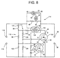
- FIGURE 8 illustrates an exemplary embodiment similar to FIGURE 7 with the addition of components to disable the timing circuit and voltage reduction circuit after completion of one full voltage reduction cycle.
- the circuit in FIGURE 8 is identical to that in FIGURE 7 with the following exceptions.
- Time delay fuse 64 and serially connected resistor 66 are inserted between the cathode of rectifier diode 120 and capacitor 122.
- the junction of resistors 124 and 134 is reconnected to the junction of fuse 64 and resistor 66.
- Resistor 68 and zener diode 70 are serially connected in the order listed between drain 44 and input ground terminal 118.
- Switch 72 is inserted with gate 74 connected to the junction of resistor 68 with zener diode 70, source 76 connected to input terminal 118, and drain 78 connected to the junction of capacitor 122 with resistor 66.
- the circuit of FIGURE 8 operates essentially identically to that of FIGURE 7, however, when switch 130 opens after approximately 30 seconds, switch 72 closes, drawing enough current to burn out fuse 64 thereby disabling the timing circuit. Future energizations of this circuit will not incur a time delay.
Landscapes
- Circuit Arrangement For Electric Light Sources In General (AREA)
- Arrangement Of Elements, Cooling, Sealing, Or The Like Of Lighting Devices (AREA)
- Circuit Arrangements For Discharge Lamps (AREA)
Abstract
Description
- The present invention relates to a lamp having compact filaments and, more particularly, to the hot shock failure mode known to occur in this type of lamp.
- With the introduction of high efficiency infrared reflective coated halogen lamps, the filament size has become more compact and, therefore, more susceptible to shock. Hot shock is a failure mode known to lamp makers where two or more primary or secondary turns of an incandescent filament touch, adhere to one another, and short out a portion of the active filament, resulting in an early burnout of the filament. Over the years, data has been collected from actual customer applications that indicate hot shock damage in this type of lamp occurs during the initial installation with the power on. As customers with hundreds of lamps complained of early hot shock failures, new lamps of the same design were installed with the power off, and the hot shock failures were greatly reduced. In a very few cases, the problem persisted due to vibration caused by construction in the area.
- Presently, the primary solution to the hot shock problem requires that the filament be designed with increased spacing between turns of the filament and/or the addition of higher levels of nitrogen. In either case, the lamp efficacy is reduced, and in many cases, the only solution is to install the lamps with the power turned off.
- Accordingly, the present invention provides an apparatus and a method to eliminate filament hot shock in lamp filaments, particularly in compact filament light sources such as high efficiency infrared reflective coated halogen lamps, during installation or during energization wherein the method comprises a voltage reduction circuit that reduces the voltage applied to the lamp filaments for a predetermined period of time and a timing circuit that is activated upon energization of the lamp and controls the predetermined period of time during which the voltage reduction circuit reduces voltage applied to the lamp filaments. The timing circuit may be activated each time the lamp is energized. Alternatively, a one time latch circuit is optionally included to enable the timing circuit upon energization and disable it once the voltage reduction circuit has operated continuously for the predetermined period of time, and forever thereafter.
- Use of the invention means that it is no longer necessary to increase the spacing between turns of the filament or to add higher levels of nitrogen to the lamp tube to minimize hot shock. Both of the aforementioned remedies reduce the efficacy of the lamp, a drawback that is eliminated by the present invention.
- Embodiments of the invention will now be described, by way of example, with reference to the accompanying drawings, in which:
- FIGURE 1 is a drawing of a typical high efficiency infrared reflective coated halogen lamp filament tube;
- FIGURE 2 is a drawing of a typical high efficiency infrared reflective coated halogen lamp installation;
- FIGURE 3 is a filament voltage graph for the lamp;
- FIGURE 4 is a drawing, partially in block form, of an improved high efficiency infrared reflective coated halogen lamp installation;
- FIGURE 5 is a filament voltage graph for the lamp of FIGURE 4;
- FIGURE 6 is a drawing of a typical high efficiency infrared reflective coated halogen lamp installation, in a second embodiment of the invention;
- FIGURE 7 is one embodiment of a delay circuit of the present invention; and,
- FIGURE 8 is a second embodiment of the delay circuit of the present invention with a one-time latch.
-
- FIGURE 1 shows a typical high efficiency infrared reflective coated halogen
lamp filament tube 10 to which the invention may be suitably applied. In one embodiment, a filament tube of this type will typically have afilament 12 approximately 10 millimeters in length consisting of 8 to 25 secondary turns. Thewall 14 of thefilament tube 10 will typically be coated so that the wall is translucent toelectromagnetic radiation 16 in the visible spectrum, however, it will reflectradiation 18 in the infrared region. The reflectedinfrared radiation 18 helps heat thefilament 12, thereby reducing power requirements for the lamp. The close spacing between turns of the filament will occasionally allow neighboring turns of the filament to contact each other if the tube is undergoing vibration such as it would encounter during installation into an energized socket. Even a momentary contact at normal operating temperatures of thefilament 12 will allow adjacent turns of thefilament 12 to weld permanently together, effectively shorting one or more turns of the filament, resulting in higher current flow, larger power consumption, overheating of thefilament 12 and consequent early failure of thefilament 12. This type of failure is referred to as a hot shock failure mode known to lamp makers where two or more primary or secondary turns of anincandescent filament 12 touch, adhere to one another, and short out the active filament, resulting in an early burnout of thefilament 12. It is of course to be understood that the present invention may also be implemented in other sizes and types of lamps which may suffer from hot shock failure due to the closeness of the filament turns. - FIGURE 2 shows a high efficiency infrared reflective coated
halogen lamp 20 that utilizes the filament tube of FIGURE 1 during installation into anenergized socket 22. As shown in FIGURE 3, avoltage 24 applied to thefilament 12 substantially instantaneously goes tofull line voltage 26 upon insertion of thelamp 20 into thesocket 22. Vibration aslamp 20 is tightened, after thefilament 12 has been energized, can cause adjacent turns of thefilament 12 to touch, resulting in the aforementioned hot shock failure mode. - Referring now to FIGURE 4, with continuing reference to FIGURES 2 and 3, a first embodiment of the invention is illustrated. The elements of FIGURE 4 are similar to those of FIGURE 2, with the exception being the addition of a
delay circuit 28 to thelamp 20. With the addition of thedelay circuit 28, thefilament voltage 24 no longer goes substantially instantaneously tofull line voltage 26. Instead, thefilament voltage 24 is reduced to approximately 40 volts for the first 30 seconds as shown in FIGURE 5, and only then is allowed to approach full line voltage. The delay circuit includes avoltage reduction circuit 29 that reduces the voltage applied to the lamp filaments for a predetermined period of time and atiming circuit 30 that is activated each time the lamp is energized. Thetiming circuit 30 controls the predetermined period of time during which thevoltage reduction circuit 29 reduces voltage applied to thelamp filament 12. - To determine an appropriate optimal voltage reduction of the
delay circuit 28, twenty (20) lamps of the same design (60PAR/HIR 120V) were tested, a sample of 5 at 120, 80, 60 and 40 volts. Each lamp was lit by a constant current supply at those voltages. The lamps were then swung on a pendulum arm against a stop. The distance was increased until a voltage drop was measured indicating hot shock. The results showed that the average distance required to hot shock increased with a reduction in voltage. At 40 volts, the distance required to hot shock the lamp deformed the filament and caused instant burnout. Forty (40) volts was consequently chosen as the optimal voltage reduction amount for thedelay circuit 28 for the described lamps (12). At 40 volts, thefilament 12 is hot enough to provide enough illumination to confirm lamp operation for the installer, but not hot enough to allow hot shock failure mode. A lower voltage is insufficient to adequately illuminate the lamp, however, reduced voltages up to 80 volts are also acceptable. -
Delay circuit 28 described above results in a short delay before full illumination of thelamp 20. This delay is not a significant drawback since this type of lamp is typically used in a commercial environment where other lamps are fully illuminated at the time. For example, a retail store may have one burned out bulb, out of many, that requires replacing, and this is usually done while the lighting circuit remains energized. If this delay is undesirable, thedelay circuit 28 can optionally further include a onetime latching circuit 32 that permanently disables the timing circuit after the voltage reduction circuit has operated, at least once, continuously for the full predetermined time period. In this way, thelamp 20 will have reduced voltage applied to thefilament 12 during initial installation but will substantially instantaneously applyfull line voltage 26 to thefilament 12 each time the lamp is turned on thereafter. - Referring now to FIGURE 6, a second embodiment of the invention is illustrated. In this embodiment, the
delay circuit 28 is incorporated into anadaptor 34. Thedelay circuit 28 incorporated into theadaptor 34 includes the samevoltage reduction circuit 29,timing circuit 30 and optional onetime latching circuit 32 as previously described. Theadaptor 34 is installed in thesame socket 22 as thestandard lamp 20 would have been installed without the invention. Operation of the second embodiment is, otherwise similar to that of the first embodiment. - Referring now to FIGURE 7, an exemplary embodiment of a delay circuit suitable for adaptation to the present invention is illustrated. The circuit comprises a
rectifier circuit 110, atimer circuit 112 and avoltage reduction circuit 114 connected in parallel withtimer circuit 112. Therectifier circuit 10 is connected betweeninput terminals rectifier diode 120 whose anode is connected toinput terminal 116 and whose cathode is connected tofilter capacitor 122 with the remaining lead ofcapacitor 122 being connected toinput terminal 118. The purpose of therectifier circuit 110 is to provide an approximately DC voltage at the junction ofrectifier circuit 110 is to provide an approximately DC voltage at the junction ofrectifier diode 120 andfilter capacitor 122 fortiming circuit 112.Timing circuit 112 includes afirst timing resistor 124, atiming capacitor 126 and asecond timing resistor 128 serially connected in the order listed between the junction ofrectifier diode 120 withfilter capacitor 122 andinput terminal 118.Timing circuit 112 further includesswitch 130,relay 132 and current limitingresistor 134, withrelay 132 comprisingenergizing coil 36 and normally closedcontacts 38. In this embodiment,switch 130 comprises a MOSFETtransistor including gate 40,source 42 anddrain 44 withgate 40 connected to the junction oftiming capacitor 126 andsecond timing resistor 128, and withsource 42 connected toinput terminal 118. Current limitingresistor 134 is first connected to the junction ofrectifier diode 120 andfilter capacitor 122 with the remaining lead connected to energizingcoil 36 whose remaining lead is connected to drain 44 ofswitch 130.Voltage reduction circuit 114 comprisesresistor 46,capacitor 48,diac 50 andthyristor 52.Resistor 46 andcapacitor 48 are serially connected in the order listed betweeninput terminal 116 andoutput terminal 54.Relay contacts 38 are also connected betweeninput terminal 116 andoutput terminal 54.Thyristor 52 includes main terminal MT1 (58), main terminal MT2 (60) andgate terminal 62 withterminal 58 connected tooutput terminal 54 and terminal 60 connected to input terminal 116.Diac 50 is connected betweengate terminal 62 and the junction ofresistor 46 withcapacitor 48. - To briefly describe the operation of the circuit of FIGURE 7, when the circuit is initially energized,
capacitor 122 quickly charges to nearly 170 volts, assuming an input voltage betweenterminals first timing resistor 124,timing capacitor 126 andsecond timing resistor 128, chargingtiming capacitor 126. This charging current creates a voltage drop sufficiently large acrosssecond timing resistor 128 to turnswitch 130 on which, in turn, causes current to flow through energizingcoil 36, openingcontacts 38. Withcontacts 38 open, current flowing betweeninput terminal 116 andoutput terminal 54 must now pass throughvoltage reducing circuit 114.Voltage reducing circuit 114 is a typical light dimming circuit whereinthyristor 52 does not turn on until sufficient charge has accumulated oncapacitor 48 to overcome the breakdown voltage ofdiac 50.Diac 50,resistor 46 andcapacitor 48 are selected such that the RMS output voltage is reduced to the desired value, 40 volts RMS in this exemplary case. Timingresistors timing capacitor 126 are selected such that the voltage drop acrosstiming resistor 128 is insufficient to keepswitch 130 turned on after approximately 30 seconds at which time current stops flowing through energizingcoil 36 allowingcontacts 38 to close and, in turn, allowing the input voltage onterminal 116 to pass unrestricted tooutput terminal 54. Timingresistors gate 40 is not exceeded.Input terminal 118 andoutput terminal 56 are interconnected and are intended to be at ground potential.Relay 132 has normally closedcontacts 38 so that, in the event of a failure inrectifier circuit 110 ortiming circuit 112, full input voltage atterminal 116 will be supplied tooutput terminal 54.Capacitor 122 can be sized sufficiently large to provide a short term memory so that momentary interruptions of the input voltage will not incur another time delay before full input voltage is reapplied tooutput terminals - FIGURE 8 illustrates an exemplary embodiment similar to FIGURE 7 with the addition of components to disable the timing circuit and voltage reduction circuit after completion of one full voltage reduction cycle. The circuit in FIGURE 8 is identical to that in FIGURE 7 with the following exceptions.
Time delay fuse 64 and serially connectedresistor 66 are inserted between the cathode ofrectifier diode 120 andcapacitor 122. The junction ofresistors fuse 64 andresistor 66.Resistor 68 andzener diode 70 are serially connected in the order listed betweendrain 44 andinput ground terminal 118.Switch 72 is inserted withgate 74 connected to the junction ofresistor 68 withzener diode 70,source 76 connected to input terminal 118, and drain 78 connected to the junction ofcapacitor 122 withresistor 66. The circuit of FIGURE 8 operates essentially identically to that of FIGURE 7, however, whenswitch 130 opens after approximately 30 seconds,switch 72 closes, drawing enough current to burn outfuse 64 thereby disabling the timing circuit. Future energizations of this circuit will not incur a time delay. - Exemplary component values for the circuits of FIGURES 7 and 8 are as follows:
Rectifier diode 120IA, 200V Filter capacitor 122 0.1µF First timing resistor 124220 megΩ Timing capacitor 126 0.06µ F Second timing resistor 12822 megΩ Switch 130 MOSFET, 200V, VG = 2V Relay 132 IA, VCOIL = 24V at 5mA Resistor 134 20kΩ Resistor 46 330kΩ Capacitor 48 0.062 µF Diac 50 32V Triac 52 IA, 200V Fuse 64 O.IA Time delay Resistor 66 ..... 220Ω Resistor 68 100kΩ Zener diode 70 12V Switch 72 MOSFET, 200V, V,=2V - There are many other timing and voltage reduction circuits known in the art that are suitable for use in the present invention. Accordingly, the present invention envisions the inclusion of any of these circuits in the embodiments according to FIGURES 7 and .
- Prior art solutions to the hot shock failure mode required the filament to be designed with increased spacing between filament turns and/or the addition of higher levels of nitrogen. In both cases, the lamp efficacy was reduced. In many cases the only solution was to install lamps with the power off. The methods disclosed above avoid the aforementioned drawbacks incurred by increasing the spacing between filament turns.
Claims (10)
- An apparatus which eliminates filament hot shock in a lamp filament during lamp installation, the apparatus comprising:a voltage reduction circuit that reduces the voltage applied to the lamp filament for a predetermined period of time; and,a timing circuit that is activated upon energization of the lamp and controls the predetermined period of time during which the voltage reduction circuit reduces voltage applied to the lamp filament.
- The apparatus of claim 1 wherein the voltage reduction circuit and the timing circuit are installed in the lamp.
- The apparatus of claim 1 wherein the voltage reduction circuit and the timing circuit are installed in an adaptor to be installed between the lamp base and a socket into which the lamp is being installed.
- The apparatus of any one of claims 1 to 3 wherein the timing circuit is activated each time the lamp is energized.
- The apparatus of any one of claims 1 to 3 including a one time latch circuit for enabling the timing circuit upon initial energization of the lamp, and for disabling the timing circuit after the voltage reduction circuit has operated for the predetermined period of time.
- The apparatus of claim 1 wherein the timing circuit activates the voltage reduction circuit for approximately 30 seconds.
- A method to eliminate filament hot shock in lamp filaments during power-on installation or during initial energization comprising:reducing the voltage applied to the lamp filaments for a predetermined period of time by use of a voltage reduction circuit; and,controlling a predetermined period of time, by a timing circuit, during which the voltage reduction circuit reduces voltage applied to the lamp filaments.
- The method of claim 7 including activating the timing circuit to reduce the voltage each time the lamp is energized.
- The method claim 7 further including the steps of:enabling, by a one time latch circuit, the timing circuit upon energization; and,disabling the timing circuit after the voltage reduction circuit has operated continuously for the predetermined period of time, and forever thereafter.
- The method of claim 7 wherein the timing circuit activates the voltage reduction circuit for approximately 30 seconds.
Applications Claiming Priority (2)
| Application Number | Priority Date | Filing Date | Title |
|---|---|---|---|
| US565252 | 2000-05-05 | ||
| US09/565,252 US6208090B1 (en) | 2000-05-05 | 2000-05-05 | Reduced voltage and time delay to eliminate filament hot shock |
Publications (1)
| Publication Number | Publication Date |
|---|---|
| EP1152644A1 true EP1152644A1 (en) | 2001-11-07 |
Family
ID=24257807
Family Applications (1)
| Application Number | Title | Priority Date | Filing Date |
|---|---|---|---|
| EP01304103A Withdrawn EP1152644A1 (en) | 2000-05-05 | 2001-05-04 | Reduced voltage and time delay to eliminate filament hot shock |
Country Status (4)
| Country | Link |
|---|---|
| US (1) | US6208090B1 (en) |
| EP (1) | EP1152644A1 (en) |
| JP (1) | JP2002015882A (en) |
| CN (1) | CN1332596A (en) |
Families Citing this family (38)
| Publication number | Priority date | Publication date | Assignee | Title |
|---|---|---|---|---|
| US6442339B1 (en) * | 2001-05-04 | 2002-08-27 | Coltene/Whaledent, Inc. | Operation of halogen lamp for curing of material |
| US7262554B2 (en) * | 2004-10-16 | 2007-08-28 | Osram Sylvania Inc. | Lamp with integral voltage converter having phase-controlled dimming circuit with hysteresis control for reducing RMS load voltage |
| US7199532B2 (en) * | 2005-02-04 | 2007-04-03 | Osram Sylvania Inc. | Lamp containing phase-control power controller with analog RMS load voltage regulation |
| US20050110432A1 (en) * | 2005-02-04 | 2005-05-26 | Osram Sylvania Inc. | Fixed reverse phase switching power supply with time-based phase pulse triggering control |
| US20050184683A1 (en) * | 2005-02-04 | 2005-08-25 | Osram Sylvania Inc. | Method of converting line voltage to an RMS load voltage in a lamp using a phase-control clipping circuit |
| US7034469B2 (en) * | 2005-02-04 | 2006-04-25 | Osram Sylvania Inc. | Phase-control power controller with analog RMS load voltage regulation |
| US7218054B2 (en) * | 2005-02-04 | 2007-05-15 | Ballenger Matthew B | Lamp having fixed phase power controller with analog trigger |
| US20050110438A1 (en) * | 2005-02-04 | 2005-05-26 | Osram Sylvania Inc. | Fixed forward phase switching power supply with time-based triggering |
| US7352134B2 (en) * | 2005-02-04 | 2008-04-01 | Osram Sylvania Inc. | Lamp containing fixed reverse phase switching power supply with time-based phase pulse triggering control |
| US20050110439A1 (en) * | 2005-02-04 | 2005-05-26 | Osram Sylvania Inc. | Method of operating a lamp containing a fixed forward phase switching power supply |
| US7211964B2 (en) * | 2005-02-04 | 2007-05-01 | Osram Sylvania Inc. | Lamp including phase-control power controller with digital RMS load voltage regulation |
| US7034473B2 (en) * | 2005-02-04 | 2006-04-25 | Osram Sylvania Inc. | Phase-control power controller for converting a line voltage to an RMS load voltage |
| US7224151B2 (en) * | 2005-02-04 | 2007-05-29 | Osram Sylvania Inc. | Fixed phase power controller with analog trigger |
| US20060175980A1 (en) * | 2005-02-04 | 2006-08-10 | Osram Sylvania Inc. | Lamp with built-in voltage converter including a bidirectional thyristor diode (SIDAC) |
| US7030567B2 (en) * | 2005-02-04 | 2006-04-18 | Osram Sylvania Inc. | Phase-control power controller with digital RMS load voltage regulation |
| US7274149B2 (en) * | 2005-02-04 | 2007-09-25 | Osram Sylvania Inc. | Lamp with integral pulse width modulated voltage control circuit |
| US7224130B2 (en) | 2005-02-04 | 2007-05-29 | Osram Sylvania Inc. | Method of operating a lamp containing a fixed phase power controller |
| US7291984B2 (en) * | 2005-02-04 | 2007-11-06 | Osram Sylvania Inc. | Method of reducing RMS load voltage in a lamp using pulse width modulation |
| US7274148B2 (en) * | 2005-02-04 | 2007-09-25 | Osram Sylvania Inc. | Lamp having fixed forward phase switching power supply with time-based triggering |
| US7116062B2 (en) * | 2005-04-01 | 2006-10-03 | Osram Sylvania Inc. | Method of soft-starting a switching power supply including pulse width modulation circuit |
| US7196480B2 (en) * | 2005-04-01 | 2007-03-27 | Osram Sylvania Inc. | Method of soft-starting a switching power supply containing phase-control clipping circuit |
| US7049758B2 (en) * | 2005-04-01 | 2006-05-23 | Osram Sylvania Inc. | Method of soft-starting a switching power supply having time-based pulse triggering control |
| US7342359B2 (en) * | 2005-04-01 | 2008-03-11 | Kendrick George B | Forward/reverse hybrid switching power supply with time-based pulse triggering control |
| US20050162095A1 (en) * | 2005-04-01 | 2005-07-28 | Osram Sylvania Inc. | Method of converting a line voltage to an RMS load voltage independently of variations in line voltage magnitude |
| US7459861B2 (en) * | 2005-04-01 | 2008-12-02 | Osram Sylvania Inc. | Lamp containing voltage conversion circuit including forward/reverse hybrid phase-control clipping circuit |
| US7053562B2 (en) * | 2005-04-01 | 2006-05-30 | Osram Sylvania Inc. | Lamp containing soft-start power supply |
| US7166964B2 (en) * | 2005-06-15 | 2007-01-23 | Osram Sylvania Inc. | Lamp containing pulse width modulated voltage conversion circuit |
| US7049750B1 (en) | 2005-06-15 | 2006-05-23 | Osram Sylvania Inc. | Lamp having integral voltage controller |
| US7170236B2 (en) * | 2005-06-15 | 2007-01-30 | Osram Sylvania Inc. | Method of setting desired RMS load voltage in a lamp |
| US7170231B2 (en) * | 2005-06-15 | 2007-01-30 | Osram Sylvania Inc. | Lamp that sets desired RMS load voltage with variable pulse width modulation |
| US7358689B1 (en) | 2006-09-25 | 2008-04-15 | Osram Sylvania Inc. | Phase-control power controller for converting a line voltage to a RMS load voltage |
| US20080122378A1 (en) * | 2006-09-25 | 2008-05-29 | Osram Sylvania Inc. | Lamp having a power supply with RMS voltage regulated output |
| US20080122377A1 (en) * | 2006-09-25 | 2008-05-29 | Osram Sylvania Inc. | Method of operating a lamp having a power supply with RMS voltage regulated output |
| US7375475B2 (en) * | 2006-10-02 | 2008-05-20 | Osram Sylvania Inc. | Lamp containing power controller having current limited RMS regulated output |
| US7462996B2 (en) * | 2006-10-02 | 2008-12-09 | Osram Sylvania Inc. | Method of operating a lamp with a power controller having current limited RMS regulated output |
| US7301291B1 (en) | 2006-10-02 | 2007-11-27 | Osram Sylvania Inc. | Power controller having current limited RMS regulated output |
| JP2013069859A (en) * | 2011-09-22 | 2013-04-18 | Toshiba Corp | Semiconductor device |
| US10071256B2 (en) * | 2016-12-12 | 2018-09-11 | Revive Solutions, Inc. | Defibrillator |
Citations (3)
| Publication number | Priority date | Publication date | Assignee | Title |
|---|---|---|---|---|
| US4547704A (en) * | 1983-08-01 | 1985-10-15 | General Electric Company | Higher efficiency incandescent lighting units |
| US4743803A (en) * | 1987-05-15 | 1988-05-10 | General Electric Company | General service tungsten-halogen incandescent lamp having improved filament shock resistance |
| US5691605A (en) * | 1995-03-31 | 1997-11-25 | Philips Electronics North America | Electronic ballast with interface circuitry for multiple dimming inputs |
Family Cites Families (2)
| Publication number | Priority date | Publication date | Assignee | Title |
|---|---|---|---|---|
| US4473776A (en) * | 1982-06-11 | 1984-09-25 | General Electric Company | Disconnect means for capacitor ballast incandescent lamp |
| US4480212A (en) * | 1982-06-14 | 1984-10-30 | Diolight Technology, Inc. | Extended life incandescent lamp with self contained diode and reflector |
-
2000
- 2000-05-05 US US09/565,252 patent/US6208090B1/en not_active Expired - Fee Related
-
2001
- 2001-05-01 JP JP2001133747A patent/JP2002015882A/en not_active Withdrawn
- 2001-05-04 EP EP01304103A patent/EP1152644A1/en not_active Withdrawn
- 2001-05-08 CN CN01119223A patent/CN1332596A/en active Pending
Patent Citations (3)
| Publication number | Priority date | Publication date | Assignee | Title |
|---|---|---|---|---|
| US4547704A (en) * | 1983-08-01 | 1985-10-15 | General Electric Company | Higher efficiency incandescent lighting units |
| US4743803A (en) * | 1987-05-15 | 1988-05-10 | General Electric Company | General service tungsten-halogen incandescent lamp having improved filament shock resistance |
| US5691605A (en) * | 1995-03-31 | 1997-11-25 | Philips Electronics North America | Electronic ballast with interface circuitry for multiple dimming inputs |
Also Published As
| Publication number | Publication date |
|---|---|
| JP2002015882A (en) | 2002-01-18 |
| CN1332596A (en) | 2002-01-23 |
| US6208090B1 (en) | 2001-03-27 |
Similar Documents
| Publication | Publication Date | Title |
|---|---|---|
| US6208090B1 (en) | Reduced voltage and time delay to eliminate filament hot shock | |
| US5623184A (en) | Lamp circuit with filament current fault monitoring means | |
| AU761194B2 (en) | Electronic ballast for at least one low-pressure discharge lamp | |
| CA1288803C (en) | Bi-level ballast circuit for operating hid lamps | |
| US5635799A (en) | Lamp protection circuit for electronic ballasts | |
| EP1696712A1 (en) | Ballast with arc protection circuit | |
| JPH0773989A (en) | 2-level lighting control system | |
| JPH0447324B2 (en) | ||
| US10959310B2 (en) | Solid-state lighting with complementary controls | |
| JP2007505464A (en) | Ballast with lampholder arc protection | |
| JPH0447957B2 (en) | ||
| US20040041524A1 (en) | Fluorescent lamp circuit | |
| US3699382A (en) | Auxiliary lighting system for arc lamp | |
| US4996463A (en) | Auxiliary lighting system for high intensity discharge lamp | |
| US3866087A (en) | Ballast circuit with integral time delay relay | |
| US5616990A (en) | Ballast scheme for a fluorescent lamp with preheated filaments | |
| US10660184B2 (en) | Solid-state lighting with multiple time delays | |
| MXPA97002947A (en) | Inductor self-regulation | |
| JPH0448589A (en) | Lighting apparatus for incandescent lamp | |
| US4143302A (en) | Energizing circuit for a fluorescent lamp | |
| US5684366A (en) | Lamp protection device | |
| KR100349318B1 (en) | Electronic starter of fluorescent lamp | |
| KR200167060Y1 (en) | Electronic starter of fluorescent lamp | |
| US20130127345A1 (en) | Anti-Flicker Apparatus for Motion Detector | |
| KR910002842Y1 (en) | Lighting circuit of fluorescent lamp |
Legal Events
| Date | Code | Title | Description |
|---|---|---|---|
| PUAI | Public reference made under article 153(3) epc to a published international application that has entered the european phase |
Free format text: ORIGINAL CODE: 0009012 |
|
| AK | Designated contracting states |
Kind code of ref document: A1 Designated state(s): AT BE CH CY DE DK ES FI FR GB GR IE IT LI LU MC NL PT SE TR Kind code of ref document: A1 Designated state(s): DE FR GB IT |
|
| AX | Request for extension of the european patent |
Free format text: AL;LT;LV;MK;RO;SI |
|
| 17P | Request for examination filed |
Effective date: 20020507 |
|
| AKX | Designation fees paid |
Free format text: DE FR GB IT |
|
| 17Q | First examination report despatched |
Effective date: 20021119 |
|
| STAA | Information on the status of an ep patent application or granted ep patent |
Free format text: STATUS: THE APPLICATION IS DEEMED TO BE WITHDRAWN |
|
| 18D | Application deemed to be withdrawn |
Effective date: 20030320 |