EP1152630A1 - An integrated multi-stage planar optical switch - Google Patents
An integrated multi-stage planar optical switch Download PDFInfo
- Publication number
- EP1152630A1 EP1152630A1 EP00401230A EP00401230A EP1152630A1 EP 1152630 A1 EP1152630 A1 EP 1152630A1 EP 00401230 A EP00401230 A EP 00401230A EP 00401230 A EP00401230 A EP 00401230A EP 1152630 A1 EP1152630 A1 EP 1152630A1
- Authority
- EP
- European Patent Office
- Prior art keywords
- optical
- optical circuit
- row
- waveguides
- optical device
- Prior art date
- Legal status (The legal status is an assumption and is not a legal conclusion. Google has not performed a legal analysis and makes no representation as to the accuracy of the status listed.)
- Withdrawn
Links
- 230000003287 optical effect Effects 0.000 title claims abstract description 125
- 238000000034 method Methods 0.000 claims description 23
- 239000000758 substrate Substances 0.000 claims description 19
- VYPSYNLAJGMNEJ-UHFFFAOYSA-N Silicium dioxide Chemical compound O=[Si]=O VYPSYNLAJGMNEJ-UHFFFAOYSA-N 0.000 claims description 12
- 239000011159 matrix material Substances 0.000 claims description 11
- 229910052710 silicon Inorganic materials 0.000 claims description 8
- 239000010703 silicon Substances 0.000 claims description 8
- 239000000463 material Substances 0.000 claims description 7
- 239000000377 silicon dioxide Substances 0.000 claims description 6
- 239000004744 fabric Substances 0.000 claims description 5
- 239000013307 optical fiber Substances 0.000 claims description 5
- 239000000853 adhesive Substances 0.000 claims description 3
- 230000001070 adhesive effect Effects 0.000 claims description 3
- 239000002861 polymer material Substances 0.000 claims description 2
- 239000004065 semiconductor Substances 0.000 claims description 2
- 230000008878 coupling Effects 0.000 claims 7
- 238000010168 coupling process Methods 0.000 claims 7
- 238000005859 coupling reaction Methods 0.000 claims 7
- 238000003466 welding Methods 0.000 claims 1
- 230000007547 defect Effects 0.000 abstract description 5
- 238000004519 manufacturing process Methods 0.000 abstract description 5
- 230000002950 deficient Effects 0.000 abstract description 4
- XUIMIQQOPSSXEZ-UHFFFAOYSA-N Silicon Chemical compound [Si] XUIMIQQOPSSXEZ-UHFFFAOYSA-N 0.000 description 7
- 230000000903 blocking effect Effects 0.000 description 5
- 239000000835 fiber Substances 0.000 description 3
- 238000012986 modification Methods 0.000 description 3
- 230000004048 modification Effects 0.000 description 3
- 230000008033 biological extinction Effects 0.000 description 2
- 230000008021 deposition Effects 0.000 description 2
- 238000005530 etching Methods 0.000 description 2
- 230000003321 amplification Effects 0.000 description 1
- 230000002238 attenuated effect Effects 0.000 description 1
- 238000005452 bending Methods 0.000 description 1
- 238000005516 engineering process Methods 0.000 description 1
- 238000001459 lithography Methods 0.000 description 1
- 238000003199 nucleic acid amplification method Methods 0.000 description 1
- 238000000206 photolithography Methods 0.000 description 1
- 230000000644 propagated effect Effects 0.000 description 1
- 238000001228 spectrum Methods 0.000 description 1
Images


Classifications
-
- G—PHYSICS
- G02—OPTICS
- G02B—OPTICAL ELEMENTS, SYSTEMS OR APPARATUS
- G02B6/00—Light guides; Structural details of arrangements comprising light guides and other optical elements, e.g. couplings
- G02B6/24—Coupling light guides
- G02B6/26—Optical coupling means
- G02B6/35—Optical coupling means having switching means
- G02B6/354—Switching arrangements, i.e. number of input/output ports and interconnection types
- G02B6/3544—2D constellations, i.e. with switching elements and switched beams located in a plane
- G02B6/3546—NxM switch, i.e. a regular array of switches elements of matrix type constellation
-
- G—PHYSICS
- G02—OPTICS
- G02B—OPTICAL ELEMENTS, SYSTEMS OR APPARATUS
- G02B6/00—Light guides; Structural details of arrangements comprising light guides and other optical elements, e.g. couplings
- G02B6/24—Coupling light guides
- G02B6/42—Coupling light guides with opto-electronic elements
- G02B6/43—Arrangements comprising a plurality of opto-electronic elements and associated optical interconnections
-
- H—ELECTRICITY
- H04—ELECTRIC COMMUNICATION TECHNIQUE
- H04Q—SELECTING
- H04Q11/00—Selecting arrangements for multiplex systems
- H04Q11/0001—Selecting arrangements for multiplex systems using optical switching
- H04Q11/0005—Switch and router aspects
-
- G—PHYSICS
- G02—OPTICS
- G02B—OPTICAL ELEMENTS, SYSTEMS OR APPARATUS
- G02B6/00—Light guides; Structural details of arrangements comprising light guides and other optical elements, e.g. couplings
- G02B6/10—Light guides; Structural details of arrangements comprising light guides and other optical elements, e.g. couplings of the optical waveguide type
- G02B6/12—Light guides; Structural details of arrangements comprising light guides and other optical elements, e.g. couplings of the optical waveguide type of the integrated circuit kind
- G02B2006/12133—Functions
- G02B2006/12145—Switch
-
- G—PHYSICS
- G02—OPTICS
- G02B—OPTICAL ELEMENTS, SYSTEMS OR APPARATUS
- G02B6/00—Light guides; Structural details of arrangements comprising light guides and other optical elements, e.g. couplings
- G02B6/24—Coupling light guides
- G02B6/26—Optical coupling means
- G02B6/35—Optical coupling means having switching means
- G02B6/3564—Mechanical details of the actuation mechanism associated with the moving element or mounting mechanism details
- G02B6/3568—Mechanical details of the actuation mechanism associated with the moving element or mounting mechanism details characterised by the actuating force
- G02B6/357—Electrostatic force
-
- G—PHYSICS
- G02—OPTICS
- G02B—OPTICAL ELEMENTS, SYSTEMS OR APPARATUS
- G02B6/00—Light guides; Structural details of arrangements comprising light guides and other optical elements, e.g. couplings
- G02B6/24—Coupling light guides
- G02B6/26—Optical coupling means
- G02B6/35—Optical coupling means having switching means
- G02B6/3564—Mechanical details of the actuation mechanism associated with the moving element or mounting mechanism details
- G02B6/3568—Mechanical details of the actuation mechanism associated with the moving element or mounting mechanism details characterised by the actuating force
- G02B6/3572—Magnetic force
-
- G—PHYSICS
- G02—OPTICS
- G02B—OPTICAL ELEMENTS, SYSTEMS OR APPARATUS
- G02B6/00—Light guides; Structural details of arrangements comprising light guides and other optical elements, e.g. couplings
- G02B6/24—Coupling light guides
- G02B6/26—Optical coupling means
- G02B6/35—Optical coupling means having switching means
- G02B6/3596—With planar waveguide arrangement, i.e. in a substrate, regardless if actuating mechanism is outside the substrate
-
- H—ELECTRICITY
- H04—ELECTRIC COMMUNICATION TECHNIQUE
- H04Q—SELECTING
- H04Q11/00—Selecting arrangements for multiplex systems
- H04Q11/0001—Selecting arrangements for multiplex systems using optical switching
- H04Q11/0005—Switch and router aspects
- H04Q2011/0007—Construction
- H04Q2011/0024—Construction using space switching
-
- H—ELECTRICITY
- H04—ELECTRIC COMMUNICATION TECHNIQUE
- H04Q—SELECTING
- H04Q11/00—Selecting arrangements for multiplex systems
- H04Q11/0001—Selecting arrangements for multiplex systems using optical switching
- H04Q11/0005—Switch and router aspects
- H04Q2011/0052—Interconnection of switches
- H04Q2011/0058—Crossbar; Matrix
Definitions
- the present invention relates generally to planar devices, and particularly to multi-stage planar optical circuit devices.
- the topology of an optical network may include any number of optical signal paths interconnected by a series of network nodes to form a mesh.
- the optical signal paths often employ amplifiers and gain flattening filters (GFF).
- the network nodes may include optical switches, optical cross-connects (OXC), or Add/Drop multiplexers.
- Optical signals are attenuated as they propagate through optical fiber and amplifiers are used to restore the signal strength. In erbium-doped fiber amplifiers different wavelengths undergo different degrees of amplification. GFFs are used to flatten the spectrum and produce signal uniformity.
- a reconfigurable optical switch or OXC functions to route the traffic between signal paths in the mesh.
- the Add/Drop multiplexer directs traffic carried by a trunk fiber into a tributary or local fiber.
- Planar optical circuit technology is promising because compact integrated optical devices having many optical circuits disposed on a single wafer can be fabricated.
- One area that is particularly promising relates to space division optical switches.
- Space division optical switches are key components in optical path cross-connect (OXC) systems, add-drop multiplexing (ADM), and protection switches.
- 8 x 8 and 16 x 16 strictly non-blocking integrated optical matrix switches have been demonstrated.
- the switches were implemented using low loss silica on a silicon substrate and achieved a high extinction ratio. It is envisioned that integrated optical matrix switches will ultimately enable the fabrication of a compact N x N switch fabric.
- FIG 1 is a schematic of the 8 x 8 strictly non-blocking integrated optical matrix switch 10 discussed above.
- Eight input waveguides 12 are connected to the first stage 20.
- Each stage 20 consists of eight switching units 16.
- the eighth stage 22 is connected to output waveguides 14.
- Switching unit 16 is a double Mach-Zehnder Interferometer (MZI) using a thermooptic switch actuator. MZI switching units 16 are attractive because they achieve a high extinction ratio.
- the utility of switch 10 is illustrated in Figure 1.
- Light signal (LS) is directed into input waveguide 4a and is propagated through each stage of matrix 10 by switching units 16 until it is directed out of output waveguide 7b.
- Figure 2 is an optical circuit layout of the schematic shown in Figure 1.
- Eight stages 20 are disposed on silicon substrate 30.
- Substrate 30 has a surface area of 68mm x 68mm.
- Figure 3 is a 16 x 16 version of matrix switch 10 depicted in Figure 1.
- Sixteen stages 20 are disposed on silicon substrate 30.
- Substrate 30 has a surface area of 107mm x 100mm.
- only one 16 x 16 switch can be fabricated on a 6" silicon wafer because the total length of the switching units exceeds the diameter of the wafer.
- curvature must be introduced between switching stages to accommodate N x N switching units.
- Input waveguides 12 and output waveguides 14 are also curved.
- optical circuit layout designs presented in Figure 2 and Figure 3 have several major drawbacks.
- this design can only accommodate a small number of components per wafer.
- this design provides a low wafer yield.
- a defect in one switching unit can affect the utility of the entire device.
- an isolated defect from photolithography, etching, or improper deposition of a silica layer will produce scrap or necessitate a costly repair.
- the design presented above can produce a lossy device.
- the radius of curvature of the waveguides 12, 14, and 18 must stay above a minimum threshold value to avoid high bending losses. For example, for 0.75% index step, the minimum bend radius is 5mm to achieve 0.1 dB per 90° arc.
- An improved circuit layout is needed that increases the number of components disposed on a wafer. Defective portions of the device must be readily isolated such that production defects do not render the entire device unusable. A device is needed that eliminates the problems associated with waveguide curvature between stages.
- an improved optical circuit device that eliminates the curvature between planar units.
- the number of components disposed on a wafer is increased because all of the surface area of the wafer is effectively utilized. No surface area is lost to curvature.
- Up to 16 rows of 4 stages per row can be accommodated on a single 6" wafer. This is a four-fold increase over the methods presently being used. Yield is increased because a defective row can be separated from the optical device. The remaining functional rows can be used.
- the problems associated with waveguide curvature are likewise eliminated.
- the optical device includes a first row of M optical circuit stages. Each of the M optical circuit stages is connected to an adjacent optical circuit stage by N parallel waveguides having substantially no curvature.
- the optical device also includes a second row of M optical circuit stages, each of the M optical circuit stages being connected to an adjacent optical circuit stage by N parallel waveguides having substantially no curvature.
- the first row is coupled to the second row to form a multi-stage planar device.
- N and M are integers.
- the present invention includes a method for making an optical device.
- the method includes the step of providing a planar device having a first row of M optical circuit stages.
- Each of the M optical circuit stages is connected to an adjacent optical circuit stage by N parallel waveguides having substantially no curvature.
- a second row of M optical circuit stages is disposed adjacent to the first row, each of the M optical circuit stages being connected to an adjacent optical circuit stage by N parallel waveguides having substantially no curvature, wherein N and M are integers.
- the planar device is separated into a first component and a second component, the first component including the first row, and the second component including the second row.
- the first component is coupled to the second component to form a multi-stage optical circuit.
- the present invention includes a method for fabricating an optical switch fabric.
- a substrate is provided.
- a matrix of optical circuit stages is disposed on the substrate.
- Each of the optical circuit stages is connected to an adjacent optical circuit stage by N parallel waveguides extending in a first direction to form at least one row of M optical circuit stages.
- the parallel waveguides have substantially no curvature.
- N and M are integers.
- the present invention for an optical device, and a method of fabricating an optical device includes a planar device having rows of M optical circuit stages. Each optical circuit stage is connected to an adjacent optical circuit stage by N parallel waveguides. The N parallel waveguides have substantially no curvature.
- the circuit layout of the switch fabric increases the number of components that can be disposed on a wafer. Defective portions of the device can be readily isolated such that production defects do not render the entire device unusable.
- the planar optical circuits of the present invention eliminates many of the problems associated with waveguide curvature between stages.
- Planar device 100 includes 16 rows 40 of optical circuit stages 20 disposed on silicon substrate 30. Each row 40 includes adjacent optical circuit stages 20, 22, 24, and 26. Input waveguides 12 are connected to optical circuit stage 20. Optical circuit stages 20, 22, 24, and 26 are connected to their adjacent optical circuit stages by 8 parallel waveguides 18. Parallel waveguides 18 are linear, having substantially no curvature. Optical circuit stage 26 is connected to output waveguides 14.
- Stages 20, 22, 24, and 26 may employ any optical circuit, but by way of example, the optical circuit shown in Figure 4 are double Mach-Zehnder Interferometer (MZI) switching stages using thermooptic switch actuators.
- MZI Mach-Zehnder Interferometer
- an optical circuit stage can include Y-digital optical switches, directional couplers, or MEMS devices.
- the optical circuit stages may employ various types of actuators such as electro-optic, electrostatic, magnetic, mechanical, as well as thermooptic.
- Waveguides 12, 14, and 18 may be of any suitable type but there is shown by way of example silica waveguides disposed on silicon wafer 30.
- waveguides may be implemented using polymer materials or other semiconductor materials.
- waveguides 12, 14, and 18 may be formed using common techniques of lithography, etching and silica deposition.
- an N x N strictly non-blocking integrated optical matrix switch 10 is disclosed.
- the N x N strictly non-blocking integrated optical matrix switch is fabricated by separating rows 40 and 42 (see Figure 4) into a discrete component 50 which includes the N stages 20 included in an N x N switch.
- Component 50 is further divided into sub-components 50 and 52, which correspond to row 40 and row 42, respectively.
- substrate 30 yields 16 sub-components.
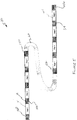
- sub-components 52 and 54 are optically coupled by connecting optical fibers 60 between output waveguides 140 and input waveguides 122.
- Input waveguides 120 are also the input waveguides of sub-component 52.
- Chip-to-chip connection 70 may be of any suitable type, but there is shown by way of example, an adhesive used to bond sub-component 52 to sub-component 54. It will be apparent to those of ordinary skill in the pertinent art that modifications and variations can be made to chip-to-chip connection 70 depending on the application.
- Laser-weld or mass pigtailing techniques can be used to connect sub-component 52 to sub-component 54, as well as aligning and mounting sub-components 52 and 54 on an alignment substrate 32.
- One of ordinary skill in the art will recognize that any number of sub-components (50, 527) can be connected end-to-end.
- N sub-components can be connected end-to-end. N being an integer number of components greater than one.
- chip-to-chip connection 70 also includes index-matching material 72 disposed in a gap between sub-component 52 and sub-component 54. Index-matching material 72 prevents optical signals from de-collimating as they propagate between output waveguides 140 and input waveguides 122.
Landscapes
- Physics & Mathematics (AREA)
- General Physics & Mathematics (AREA)
- Optics & Photonics (AREA)
- Engineering & Computer Science (AREA)
- Computer Networks & Wireless Communication (AREA)
- Mathematical Physics (AREA)
- Optical Integrated Circuits (AREA)
- Optical Modulation, Optical Deflection, Nonlinear Optics, Optical Demodulation, Optical Logic Elements (AREA)
Abstract
Description
- The present invention relates generally to planar devices, and particularly to multi-stage planar optical circuit devices.
- In general, the topology of an optical network may include any number of optical signal paths interconnected by a series of network nodes to form a mesh. The optical signal paths often employ amplifiers and gain flattening filters (GFF). The network nodes may include optical switches, optical cross-connects (OXC), or Add/Drop multiplexers. Optical signals are attenuated as they propagate through optical fiber and amplifiers are used to restore the signal strength. In erbium-doped fiber amplifiers different wavelengths undergo different degrees of amplification. GFFs are used to flatten the spectrum and produce signal uniformity. A reconfigurable optical switch or OXC functions to route the traffic between signal paths in the mesh. The Add/Drop multiplexer directs traffic carried by a trunk fiber into a tributary or local fiber.
- Currently, designers are seeking to use planar optical circuits in amplifier, GFF, OXC, and Add/Drop multiplexer implementations. Planar optical circuit technology is promising because compact integrated optical devices having many optical circuits disposed on a single wafer can be fabricated. One area that is particularly promising relates to space division optical switches. Space division optical switches are key components in optical path cross-connect (OXC) systems, add-drop multiplexing (ADM), and protection switches.
- In one approach, 8 x 8 and 16 x 16 strictly non-blocking integrated optical matrix switches have been demonstrated. The switches were implemented using low loss silica on a silicon substrate and achieved a high extinction ratio. It is envisioned that integrated optical matrix switches will ultimately enable the fabrication of a compact N x N switch fabric.
- Figure 1 is a schematic of the 8 x 8 strictly non-blocking integrated
optical matrix switch 10 discussed above. Eightinput waveguides 12 are connected to thefirst stage 20. Eachstage 20 consists of eightswitching units 16. Theeighth stage 22 is connected tooutput waveguides 14.Switching unit 16 is a double Mach-Zehnder Interferometer (MZI) using a thermooptic switch actuator. MZIswitching units 16 are attractive because they achieve a high extinction ratio. The utility ofswitch 10 is illustrated in Figure 1. Light signal (LS) is directed into input waveguide 4a and is propagated through each stage ofmatrix 10 byswitching units 16 until it is directed out of output waveguide 7b. - Figure 2 is an optical circuit layout of the schematic shown in Figure 1. Eight
stages 20 are disposed onsilicon substrate 30.Substrate 30 has a surface area of 68mm x 68mm. Thus, only one 8 x 8 switch can be fabricated on a 4" silicon wafer because the total length of the switching units exceeds the diameter of the wafer. Figure 3 is a 16 x 16 version ofmatrix switch 10 depicted in Figure 1. Sixteenstages 20 are disposed onsilicon substrate 30.Substrate 30 has a surface area of 107mm x 100mm. Likewise, only one 16 x 16 switch can be fabricated on a 6" silicon wafer because the total length of the switching units exceeds the diameter of the wafer. In both optical circuit layouts, curvature must be introduced between switching stages to accommodate N x N switching units.Input waveguides 12 andoutput waveguides 14 are also curved. - The optical circuit layout designs presented in Figure 2 and Figure 3 have several major drawbacks. First, this design can only accommodate a small number of components per wafer. Second, this design provides a low wafer yield. A defect in one switching unit can affect the utility of the entire device. Thus, an isolated defect from photolithography, etching, or improper deposition of a silica layer will produce scrap or necessitate a costly repair. Finally, the design presented above can produce a lossy device. Depending on the index step, the radius of curvature of the
waveguides - What is needed are optical circuit layouts that eliminate the aforementioned disadvantages. An improved circuit layout is needed that increases the number of components disposed on a wafer. Defective portions of the device must be readily isolated such that production defects do not render the entire device unusable. A device is needed that eliminates the problems associated with waveguide curvature between stages.
- The present invention overcomes the aforementioned disadvantages as well as others. In accordance with the teachings of the present invention, an improved optical circuit device is presented that eliminates the curvature between planar units. Thus, the number of components disposed on a wafer is increased because all of the surface area of the wafer is effectively utilized. No surface area is lost to curvature. Up to 16 rows of 4 stages per row can be accommodated on a single 6" wafer. This is a four-fold increase over the methods presently being used. Yield is increased because a defective row can be separated from the optical device. The remaining functional rows can be used. Finally, by eliminating waveguide curvature between stages, the problems associated with waveguide curvature are likewise eliminated.
- One aspect of the present invention is an optical device. The optical device includes a first row of M optical circuit stages. Each of the M optical circuit stages is connected to an adjacent optical circuit stage by N parallel waveguides having substantially no curvature. The optical device also includes a second row of M optical circuit stages, each of the M optical circuit stages being connected to an adjacent optical circuit stage by N parallel waveguides having substantially no curvature. The first row is coupled to the second row to form a multi-stage planar device. N and M are integers.
- In another aspect, the present invention includes a method for making an optical device. The method includes the step of providing a planar device having a first row of M optical circuit stages. Each of the M optical circuit stages is connected to an adjacent optical circuit stage by N parallel waveguides having substantially no curvature. A second row of M optical circuit stages is disposed adjacent to the first row, each of the M optical circuit stages being connected to an adjacent optical circuit stage by N parallel waveguides having substantially no curvature, wherein N and M are integers. The planar device is separated into a first component and a second component, the first component including the first row, and the second component including the second row. The first component is coupled to the second component to form a multi-stage optical circuit.
- In another aspect, the present invention includes a method for fabricating an optical switch fabric. A substrate is provided. A matrix of optical circuit stages is disposed on the substrate. Each of the optical circuit stages is connected to an adjacent optical circuit stage by N parallel waveguides extending in a first direction to form at least one row of M optical circuit stages. The parallel waveguides have substantially no curvature. N and M are integers.
- Additional features and advantages of the invention will be set forth in the detailed description which follows, and in part will be readily apparent to those skilled in the art from that description or recognized by practicing the invention as described herein, including the detailed description which follows, the claims, as well as the appended drawings.
- It is to be understood that both the foregoing general description and the following detailed description are merely exemplary of the invention, and are intended to provide an overview or framework for understanding the nature and character of the invention as it is claimed. The accompanying drawings are included to provide a further understanding of the invention, and are incorporated in and constitute a part of this specification. The drawings illustrate various embodiments of the invention, and together with the description serve to explain the principles and operation of the invention.
-
- Figure 1 is a schematic view of an 8 x 8 switch;
- Figure 2 is a circuit layout of the 8 x 8 switch depicted in Figure 1;
- Figure 3 is a circuit layout of a 16 x 16 version of the switch shown in Figure 1;
- Figure 4 is a matrix of optical circuit stages disposed on a wafer in accordance with the present invention;
- Figure 5 is an example of an 8 x 8 optical circuit using optical fiber connections in accordance with the present invention; and
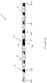
- Figure 6 is an example of an 8 x 8 switch using a chip-to-chip connection in accordance with the present invention.
-
- Reference will now be made in detail to the present preferred embodiments of the invention, examples of which are illustrated in the accompanying drawings. Wherever possible, the same reference numbers will be used throughout the drawings to refer to the same or like parts. An exemplary embodiment of the optical device of the present invention is shown in Figure 4, and is designated generally throughout by reference numeral 100.
- In accordance with the invention, the present invention for an optical device, and a method of fabricating an optical device, includes a planar device having rows of M optical circuit stages. Each optical circuit stage is connected to an adjacent optical circuit stage by N parallel waveguides. The N parallel waveguides have substantially no curvature. The circuit layout of the switch fabric increases the number of components that can be disposed on a wafer. Defective portions of the device can be readily isolated such that production defects do not render the entire device unusable. The planar optical circuits of the present invention eliminates many of the problems associated with waveguide curvature between stages.
- As embodied herein, and depicted in Figure 4, a planar optical device according to the present invention is disclosed. Planar device 100 includes 16
rows 40 of optical circuit stages 20 disposed onsilicon substrate 30. Eachrow 40 includes adjacent optical circuit stages 20, 22, 24, and 26.Input waveguides 12 are connected tooptical circuit stage 20. Optical circuit stages 20, 22, 24, and 26 are connected to their adjacent optical circuit stages by 8parallel waveguides 18.Parallel waveguides 18 are linear, having substantially no curvature.Optical circuit stage 26 is connected tooutput waveguides 14. -
Stages Waveguides silicon wafer 30. One of ordinary skill in the art will recognize that waveguides may be implemented using polymer materials or other semiconductor materials. As a nonlimiting example,waveguides - In Figure 4, 64 switching stages are accommodated by
substrate 30. One of ordinary skill in the art will recognize that the number of rows (40, 42,...44) the number ofstages 20, and the number ofwaveguides substrate 30 may vary depending on the N x N switch design (N being equal to 2y, y being an integer), size ofsubstrate 30 and the width of switchingstage 20. - As embodied herein and depicted in Figure 5, an N x N strictly non-blocking integrated
optical matrix switch 10 is disclosed. The N x N strictly non-blocking integrated optical matrix switch is fabricated by separatingrows 40 and 42 (see Figure 4) into a discrete component 50 which includes the N stages 20 included in an N x N switch. Component 50 is further divided intosub-components 50 and 52, which correspond to row 40 androw 42, respectively. Thus,substrate 30yields 16 sub-components. Referring back to Figure 5, sub-components 52 and 54 are optically coupled by connectingoptical fibers 60 betweenoutput waveguides 140 andinput waveguides 122.Input waveguides 120 are also the input waveguides ofsub-component 52. - As embodied herein and depicted in Figure 6, an alternate embodiment of the N x N strictly non-blocking integrated
optical matrix switch 10 of the present invention is disclosed. In this example, sub-components 52 and 54 are optically coupled using chip-to-chip connection 70 betweenoutput waveguides 140 andinput waveguides 122. Chip-to-chip connection 70 may be of any suitable type, but there is shown by way of example, an adhesive used to bond sub-component 52 to sub-component 54. It will be apparent to those of ordinary skill in the pertinent art that modifications and variations can be made to chip-to-chip connection 70 depending on the application. Laser-weld or mass pigtailing techniques can be used to connect sub-component 52 to sub-component 54, as well as aligning and mountingsub-components alignment substrate 32. One of ordinary skill in the art will recognize that any number of sub-components (50, 52...) can be connected end-to-end. Thus, instead of connecting two sub-components end-to-end, N sub-components can be connected end-to-end. N being an integer number of components greater than one. - In another alternative embodiment of the invention, as embodied herein and as shown in Figure 6, chip-to-chip connection 70 also includes index-matching material 72 disposed in a gap between
sub-component 52 andsub-component 54. Index-matching material 72 prevents optical signals from de-collimating as they propagate betweenoutput waveguides 140 andinput waveguides 122. - It will be apparent to those skilled in the art that various modifications and variations can be made to the present invention without departing from the spirit and scope of the invention. Thus, it is intended that the present invention cover the modifications and variations of this invention provided they come within the scope of the appended claims and their equivalents.
Claims (36)
- An optical device, comprising:a first row of M optical circuit stages, each of the M optical circuit stages being connected to an adjacent optical circuit stage by N parallel waveguides having substantially no curvature; anda second row of M optical circuit stages, each of the M optical circuit stages being connected to an adjacent optical circuit stage by N parallel waveguides having substantially no curvature, wherein the first row is coupled to the second row to form a multi-stage planar device, and N and M are integers.
- The optical device of claim 1, wherein each of the M optical circuit stages includes N-optical circuit units to form an N x N multi-stage planar device.
- The optical device of claim 2, wherein the optical circuit unit includes a switching device.
- The optical device of claim 3, wherein the switching device includes a Mach-Zehnder switch.
- The optical device of claim 3, wherein the switching device includes a Y-digital optical switch.
- The optical device of claim 2, wherein each optical circuit unit includes a directional coupler.
- The optical device of claim 2, wherein each optical circuit unit includes a MEMS device.
- The optical device of claim 2, wherein each optical circuit unit includes a thermooptical actuator.
- The optical device of claim 2, wherein each optical circuit unit includes a mechanical actuator.
- The optical device of claim 2, wherein each optical circuit unit includes an electro-optical actuator.
- The optical device of claim 2, wherein each optical circuit unit includes an electrostatic actuator.
- The optical device of claim 2, wherein each optical circuit unit includes a magnetic actuator.
- The optical device of claim 2, wherein each optical circuit unit includes a electro-optical actuator.
- The optical device of claim 1, wherein the first row is coupled to the second row by optical fibers.
- The optical device of claim 1, wherein the first row is connected to the second row by a chip-to-chip connection.
- The optical device of claim 15, wherein the chip-to-chip connection includes a laser weld.
- The optical device of claim 15, wherein the chip-to-chip connection includes an adhesive.
- The optical device of claim 15, wherein the chip-to-chip connection is implemented using a mass pigtailing technique.
- The optical device of claim 15, wherein the chip-to-chip connection includes aligning and mounting the first row and the second row on an alignment substrate.
- The optical device of claim 15, wherein index-matching material is disposed between the first row and the second row.
- A method for making an optical device comprising the steps of:providing a planar device having a plurality of rows, each of the plurality of rows having M optical circuit stages, each of the M optical circuit stages being connected to an adjacent optical circuit stage by N parallel waveguides having substantially no curvature, wherein N and M are integers;separating the planar device into a plurality of discrete components, wherein each discrete component includes a row of the plurality of rows; andcoupling the plurality of discrete components to form a multi-stage planar device.
- The method of claim 21, wherein the step of providing includes providing each component with N input waveguides and N output waveguides.
- The method of claim 22, wherein the step of coupling includes connecting the N output waveguides of a discrete component to the N input waveguides of an adjacent discrete component with optical fiber.
- The method of claim 22, wherein the step of coupling includes connecting the N output waveguides of a discrete component to the N input waveguides of an adjacent discrete component using a chip-to-chip connection.
- The method of claim 22, wherein the step of coupling includes connecting the N output waveguides of a discrete component to the N input waveguides of an adjacent discrete component by laser welding.
- The method of claim 22, wherein the step of coupling includes connecting the N output waveguides of a discrete component to the N input waveguides of an adjacent discrete component using an adhesive.
- The method of claim 22, wherein the step of coupling includes disposing index-matching material between adjacent discrete components.
- The method of claim 21, wherein the planar device is an N x N switch fabric.
- A method for fabricating an optical circuit fabric comprising the steps of:providing a substrate;disposing a matrix of optical circuit stages on the substrate, each of the optical circuit stages being connected to an adjacent optical circuit stage by N parallel waveguides extending in a first direction to form at least one row of M optical circuit stages, wherein the parallel waveguides have substantially no curvature, and N and M are integers.
- The method of claim 29, further comprising the steps of:separating the at least one row of M-optical circuit stages into a plurality of optical circuit components; andcoupling the plurality of optical circuit components to form a multi-stage planar device.
- The method of claim 29, wherein the substrate is comprised of silicon.
- The method of claim 29, wherein the substrate is comprised of silica.
- The method of claim 29, wherein the waveguides are comprised of a silica material.
- The method of claim 29, wherein the waveguides are comprised of a polymer material.
- The method of claim 29, wherein the waveguides are comprised of a semiconductor material.
- The method of claim 29, wherein the substrate has an approximate surface area of 100mm x 100mm.
Priority Applications (1)
| Application Number | Priority Date | Filing Date | Title |
|---|---|---|---|
| EP00401230A EP1152630A1 (en) | 2000-05-05 | 2000-05-05 | An integrated multi-stage planar optical switch |
Applications Claiming Priority (1)
| Application Number | Priority Date | Filing Date | Title |
|---|---|---|---|
| EP00401230A EP1152630A1 (en) | 2000-05-05 | 2000-05-05 | An integrated multi-stage planar optical switch |
Publications (1)
| Publication Number | Publication Date |
|---|---|
| EP1152630A1 true EP1152630A1 (en) | 2001-11-07 |
Family
ID=8173668
Family Applications (1)
| Application Number | Title | Priority Date | Filing Date |
|---|---|---|---|
| EP00401230A Withdrawn EP1152630A1 (en) | 2000-05-05 | 2000-05-05 | An integrated multi-stage planar optical switch |
Country Status (1)
| Country | Link |
|---|---|
| EP (1) | EP1152630A1 (en) |
Cited By (3)
| Publication number | Priority date | Publication date | Assignee | Title |
|---|---|---|---|---|
| WO2008157248A1 (en) * | 2007-06-14 | 2008-12-24 | Adc Telecommunication, Inc. | Fiber optic module |
| CN101216603B (en) * | 2008-01-09 | 2010-06-02 | 北京邮电大学 | An Integrated Multilevel Two-Dimensional Optical MEMS Optical Switch |
| WO2025032677A1 (en) * | 2023-08-07 | 2025-02-13 | 日本電信電話株式会社 | Optical switch |
Citations (3)
| Publication number | Priority date | Publication date | Assignee | Title |
|---|---|---|---|---|
| JPS62283794A (en) * | 1986-05-30 | 1987-12-09 | Nec Corp | Matrix switching system for communication system |
| DE19702743A1 (en) * | 1997-01-15 | 1998-07-23 | Siemens Ag | Integrated optical switching arrangement |
| EP0933963A2 (en) * | 1998-01-30 | 1999-08-04 | Jds Fitel Inc. | Optical variable-ratio power splitter and optical switches |
-
2000
- 2000-05-05 EP EP00401230A patent/EP1152630A1/en not_active Withdrawn
Patent Citations (3)
| Publication number | Priority date | Publication date | Assignee | Title |
|---|---|---|---|---|
| JPS62283794A (en) * | 1986-05-30 | 1987-12-09 | Nec Corp | Matrix switching system for communication system |
| DE19702743A1 (en) * | 1997-01-15 | 1998-07-23 | Siemens Ag | Integrated optical switching arrangement |
| EP0933963A2 (en) * | 1998-01-30 | 1999-08-04 | Jds Fitel Inc. | Optical variable-ratio power splitter and optical switches |
Non-Patent Citations (3)
| Title |
|---|
| HINO S ET AL: "A COMPACT TERABIT-CLASS ATM SWITCHING FABRIC USING A 20-GB/S SUBNETWORK LSI AND FREE-SPACE OTPICAL INTERCONNECTIONS", ISS. WORLD TELECOMMUNICATIONS CONGRESS. (INTERNATIONAL SWITCHING SYMPOSIUM),CA,TORONTO, PINNACLE GROUP, 21 September 1997 (1997-09-21), pages 223 - 229, XP000720527 * |
| MINORU AKIYAMA ET AL: "PHOTONIC SWITCHING SYSTEM", IEICE TRANSACTIONS,JP,INSTITUTE OF ELECTRONICS INFORMATION AND COMM. ENG. TOKYO, vol. E74, no. 1, 1991, pages 84 - 91, XP000230386, ISSN: 0917-1673 * |
| PATENT ABSTRACTS OF JAPAN vol. 012, no. 177 (E - 613) 25 May 1988 (1988-05-25) * |
Cited By (5)
| Publication number | Priority date | Publication date | Assignee | Title |
|---|---|---|---|---|
| WO2008157248A1 (en) * | 2007-06-14 | 2008-12-24 | Adc Telecommunication, Inc. | Fiber optic module |
| US7899295B2 (en) | 2007-06-14 | 2011-03-01 | Adc Telecommunications, Inc. | Fiber optic module |
| US8238708B2 (en) | 2007-06-14 | 2012-08-07 | Adc Telecommunications, Inc. | Fiber optic module |
| CN101216603B (en) * | 2008-01-09 | 2010-06-02 | 北京邮电大学 | An Integrated Multilevel Two-Dimensional Optical MEMS Optical Switch |
| WO2025032677A1 (en) * | 2023-08-07 | 2025-02-13 | 日本電信電話株式会社 | Optical switch |
Similar Documents
| Publication | Publication Date | Title |
|---|---|---|
| US7974502B2 (en) | Optical module and optical switch | |
| US7469080B2 (en) | Modular all-optical cross-connect | |
| US6801679B2 (en) | Multifunctional intelligent optical modules based on planar lightwave circuits | |
| US20020181855A1 (en) | Electrically controllable integrated optical cross-connect | |
| CN109844589A (en) | The optical switch based on silicon photon with low polarization sensitivity | |
| US12235492B2 (en) | Wafer-scale-integrated silicon-photonics-based optical switching system and method of forming | |
| CN117043650A (en) | Low-loss, low-crosstalk optical mode multiplexers and optical cross-connects | |
| EP1218781A1 (en) | Hybrid integrated optical add-drop multiplexer | |
| US20040184709A1 (en) | MEMS waveguide shuttle optical latching switch | |
| JPH10227936A (en) | Hybrid planar optical circuit and its fabrication method | |
| US6519059B1 (en) | Wavelength division add/drop multiplexer | |
| JP3151699B2 (en) | Fabrication method of optical circuit components | |
| Tumolillo et al. | Solid state optical space switches for network cross-connect and protection applications | |
| JP4776082B2 (en) | Planar optical waveguide type Mach-Zehnder circuit, planar optical waveguide circuit and optical multiplexer / demultiplexer using the planar optical waveguide type Mach-Zehnder circuit | |
| US20020191896A1 (en) | Integrated multi-stage planar device | |
| CA2386352A1 (en) | Nxn optical matrix switch using modified cross-connect of 1xn switches | |
| JP3042664B2 (en) | Optical frequency selection switch | |
| US11194093B2 (en) | Optical switch array and multicast switch | |
| JP2000329954A (en) | Array waveguide grating | |
| US6748130B2 (en) | Optical switch and using method therefor | |
| CN1243995C (en) | Photo passive device adopting multilayer optical waveguide and basing on array waveguide waveguide interference device | |
| Kozhevnikov et al. | Integrated array of 1× N optical switches for wavelength-independent and WDM applications | |
| Ooba et al. | Planar-waveguide-type optical switching devices | |
| CA2361509A1 (en) | High-performance nxn optical matrix switch using double-size butterfly network of 2x2 switching units | |
| Lipscomb et al. | Applications of Organic and Inorganic Optical Thin Films in Telecommunications |
Legal Events
| Date | Code | Title | Description |
|---|---|---|---|
| PUAI | Public reference made under article 153(3) epc to a published international application that has entered the european phase |
Free format text: ORIGINAL CODE: 0009012 |
|
| AK | Designated contracting states |
Kind code of ref document: A1 Designated state(s): FR Kind code of ref document: A1 Designated state(s): AT BE CH CY DE DK ES FI FR GB GR IE IT LI LU MC NL PT SE |
|
| AX | Request for extension of the european patent |
Free format text: AL;LT;LV;MK;RO;SI |
|
| AKX | Designation fees paid |
Free format text: FR |
|
| REG | Reference to a national code |
Ref country code: DE Ref legal event code: 8566 |
|
| STAA | Information on the status of an ep patent application or granted ep patent |
Free format text: STATUS: THE APPLICATION IS DEEMED TO BE WITHDRAWN |
|
| 18D | Application deemed to be withdrawn |
Effective date: 20020508 |