EP1152556A2 - Self-aligning infra-red communication link - Google Patents
Self-aligning infra-red communication link Download PDFInfo
- Publication number
- EP1152556A2 EP1152556A2 EP01101824A EP01101824A EP1152556A2 EP 1152556 A2 EP1152556 A2 EP 1152556A2 EP 01101824 A EP01101824 A EP 01101824A EP 01101824 A EP01101824 A EP 01101824A EP 1152556 A2 EP1152556 A2 EP 1152556A2
- Authority
- EP
- European Patent Office
- Prior art keywords
- actuator
- mirror
- light signal
- optical port
- outgoing light
- Prior art date
- Legal status (The legal status is an assumption and is not a legal conclusion. Google has not performed a legal analysis and makes no representation as to the accuracy of the status listed.)
- Granted
Links
- 238000004891 communication Methods 0.000 title description 24
- 230000003287 optical effect Effects 0.000 claims abstract description 16
- 230000005540 biological transmission Effects 0.000 claims abstract description 11
- 230000004044 response Effects 0.000 claims abstract description 6
- 239000000758 substrate Substances 0.000 description 13
- 238000013461 design Methods 0.000 description 8
- 230000008901 benefit Effects 0.000 description 4
- 238000006073 displacement reaction Methods 0.000 description 4
- 230000007423 decrease Effects 0.000 description 3
- 238000000034 method Methods 0.000 description 3
- 229910021420 polycrystalline silicon Inorganic materials 0.000 description 3
- 229920005591 polysilicon Polymers 0.000 description 3
- 230000008569 process Effects 0.000 description 3
- 230000011664 signaling Effects 0.000 description 3
- 230000009471 action Effects 0.000 description 2
- 230000008859 change Effects 0.000 description 2
- 230000006872 improvement Effects 0.000 description 2
- 230000003993 interaction Effects 0.000 description 2
- 238000010845 search algorithm Methods 0.000 description 2
- XUIMIQQOPSSXEZ-UHFFFAOYSA-N Silicon Chemical compound [Si] XUIMIQQOPSSXEZ-UHFFFAOYSA-N 0.000 description 1
- 230000000712 assembly Effects 0.000 description 1
- 238000000429 assembly Methods 0.000 description 1
- 239000011248 coating agent Substances 0.000 description 1
- 238000000576 coating method Methods 0.000 description 1
- 238000012790 confirmation Methods 0.000 description 1
- 238000005530 etching Methods 0.000 description 1
- 230000006870 function Effects 0.000 description 1
- PCHJSUWPFVWCPO-UHFFFAOYSA-N gold Chemical compound [Au] PCHJSUWPFVWCPO-UHFFFAOYSA-N 0.000 description 1
- 239000010931 gold Substances 0.000 description 1
- 229910052737 gold Inorganic materials 0.000 description 1
- 238000012986 modification Methods 0.000 description 1
- 230000004048 modification Effects 0.000 description 1
- 230000006855 networking Effects 0.000 description 1
- 238000005457 optimization Methods 0.000 description 1
- 238000012545 processing Methods 0.000 description 1
- 229910052710 silicon Inorganic materials 0.000 description 1
- 239000010703 silicon Substances 0.000 description 1
- 238000012360 testing method Methods 0.000 description 1
- 238000012546 transfer Methods 0.000 description 1
Images



Classifications
-
- H—ELECTRICITY
- H04—ELECTRIC COMMUNICATION TECHNIQUE
- H04B—TRANSMISSION
- H04B10/00—Transmission systems employing electromagnetic waves other than radio-waves, e.g. infrared, visible or ultraviolet light, or employing corpuscular radiation, e.g. quantum communication
- H04B10/11—Arrangements specific to free-space transmission, i.e. transmission through air or vacuum
Definitions
- the present invention relates to light based communication links, and more particularly, to a self-aligning communication link for connecting computer-based devices.
- Infra-red (IR) communication links are now provided on many computers and devices designed to communicate with computers or with each other.
- An IR communication link utilizes an IR transmitter and receiver on each device for sending and receiving digital light signals, respectively.
- Each IR module consists of an IR transmitter, typically a light emitting diode, a photodiode, used to receive the light signals, and electronic circuitry for signal processing and control.
- the three components are small, relatively simple, and produced in high volumes. Hence, the IR module is generally a very inexpensive component.
- the user aligns the two devices such that the IR transmitter in the first device is aligned with the IR receiver in the second device.
- IR communication links provide an attractive alternative to wires for connecting these devices both in terms of cost and convenience.
- digital cameras typically include an IR communication link for downloading pictures taken by the camera to a computer.
- IR communication links have also been used for connecting computers together in networking systems and computers to printers.
- IR communication links have great potential, they have not found wide acceptance among users.
- the IR transmitter and receiver of the first device must be aligned with the corresponding receiver and transmitter of the second device.
- the devices In practice, the devices must be aligned to within 20 degrees both horizontally and vertically. This often requires more time and effort than most users are willing to invest. Hence, the IR communication links are seldom used.
- the alignment tolerance must be even greater.
- the light emitting diodes (LEDs) used to generate the IR light signals have an intensity distribution that decreases with the angle from the central ray of the light beam.
- LEDs light emitting diodes
- the maximum communication distance is determined by the light intensity available to each device.
- mis-aligned devices have reduced range.
- the intensity of the transmitters in the IR devices can be increased; however, various safety, battery-life, and cost considerations limit the maximum intensity of the light beam. Accordingly, devices that are mis-aligned by 20 degrees are limited to a communication path of less than one meter.
- the present invention is an optical port with directional control.
- the port includes a transmitter, receiver, and first actuator.
- the transmitter generates an outgoing light signal that propagates in a transmission direction in response to an outgoing electrical signal.
- the receiver receives an incoming light signal and generating an incoming electrical signal therefrom, the receiver having a reception direction aligned with the transmission direction.
- the first actuator alters the transmission direction of the outgoing light signal in response to a first control signal.
- the first actuator determines the direction of the outgoing light signal in a first plane
- a second actuator controls the direction of the outgoing light signal by an amount determined by a second control signal.
- the second actuator controls the direction of the outgoing light signal in a second plane that is orthogonal to the first plane.
- the actuators can be constructed from beam deflectors that utilize moveable mirrors to alter the transmission direction.
- the deflector includes an array of mirrors, each mirror rotating about an axis through the mirror. Actuators that rotate the transmitter and reflector may also be utilized.
- the LEDs used to generate the light signals transmitted by an IR communication link have an intensity distribution that is shown in Figure 1.
- the opening angle 12 of the light cone from a typical LED 11 is approximately 20 degrees.
- the radial intensity distribution of this cone is shown at 13.
- Each device includes an LED for transmitting light signals and a photodiode for receiving light signals generated by the device at the other end of the communication link.
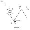
- Port 20 includes a transmitter/receiver pair 21 comprising an LED 23 and a photodiode 22.
- the light generated by LED 23 is reflected off of a first mirror 24 that can be rotated about axis 25 and a second mirror 26 that can be rotated about an orthogonal axis 27.
- the light beam from LED 23 can be directed within a range of output angles in both the horizontal and vertical directions.
- light received by mirror 26 along an angle defined by the positions of mirrors 24 and 26 will be reflected onto photodiode 22.
- the manner in which mirrors 24 and 26 are constructed will be explained in more detail below.
- each IR port includes a controller that operates the various mirrors and monitors the signals received on the receiver in the port.
- IR port number 1 initiates the connection.
- IR port number 1 may be connected to a computer that is running a program which utilizes the IR port for communication with another device and that program has initiated a data transfer.
- the protocol used to establish and optimize the communication link involves multiple interactions between the two ports as well as multiple scenarios that depend on their relative positions.
- This complex algorithm is easier understood with the aid of the flow charts shown in Figures 3A-B.
- the logical dependencies are shown in solid lines, and the optical signals between the ports are shown in dashed lines.
- the flow chart for the actions taken by port 1 is shown at 101, and the flow chart for the actions taken by port 2 is shown at 102.
- the first part of the algorithm, shown in Figure 3A brings the ports into sufficient alignment to establish a handshake between the communicating ports. It assumes that both ports are misaligned such that each is out of the angular range of the other.
- the protocol proceeds generally in the following manner:
- FIG. 3B is a flow chart of the algorithm carried out by each port during optimization.
- the flow-chart for the operations carried out by port 1 is shown at 151, and the flow chart for the operations carried out by port 2 is shown at 152.
- the algorithm proceeds as follows:
- the signaling protocol can be carried out at a relatively low frequency and still provide satisfactory performance as measured by the time needed to complete the alignment process. For example, if each beam has 5 positions, each port requires 25 attempts at handshaking. An alignment time of the order of one second is more than adequate for most applications. Hence, the system can utilize a signaling protocol that takes 20 msec. per handshaking attempt. Accordingly, the signal-to-noise ratio can be improved during the alignment process by utilizing long pulses for the signaling.
- the goal of the search algorithm is to determine the mirror positions in each IR port that provide the maximum signal strength for communications between the two IR ports.
- the number of mirror positions at which a handshaking protocol can be successfully completed will depend on the number of discrete positions that each mirror can occupy. If this number is relatively small, there will only be one or two positions at which the handshaking protocol will succeed. As the number increases, the angular step size of the search algorithm decreases, and hence, a number of "acceptable" positions may be present.
- the acceptable positions will, in general, define a cone of angles within which acceptable signal strength is present.
- the mirror positions at the center of this cone will, in general, also be the position of maximum signal strength.
- the angular coverage of the IR port described above depends on the ability to deflect the beam at relatively large angles. For example, in order to increase the angular coverage from the standard 20 degrees to 60 degrees, the beam should be deflected by 20 degrees in each direction. If mirrors are used to deflect the beam, then a 10-degree rotation of the mirror will produce the required 20 degree beam deflection. For this application, each mirror needs to have a reflective area of at least 1 square millimeter.
- IR modules are inherently low-cost, miniature, devices
- the present invention requires an inexpensive, preferably micromachined, mirror design.
- micromachined rotating mirror designs known to the art; however, low-cost designs are limited to mirror sizes and angles of rotation far below the required values, while large-size, large-angle designs would impose unacceptable costs if utilized in the present invention.
- the requirements of large mirror size and large angles of rotation are mutually exclusive in low-cost, electrostatically actuated, mirror designs operating at reasonable actuation voltages.
- Figures 4 and 5 describe a novel mirror design that takes advantage of the fact that beam coherence is not required in IR communications, and, therefore, one large mirror can be replaced with a multiplicity of small mirrors moving synchronously.
- the conflict between large size and the large angle of rotation is resolved by dividing the required area of the mirror into a plurality of small elongated mirror elements, each of which is sufficiently narrow to allow the required rotation.
- Figure 4 is a top view of a portion of a micro-machined mirror assembly 30, and
- Figure 5 is a cross-sectional view through line 38-39 shown in Figure 4.
- Mirror assembly 30 is constructed from a plurality of micro-machined mirrors 32 that have been etched from a substrate 35 that is bonded to a second substrate 37.
- Each mirror is connected to substrate 35 via a flexible link 31 that allows the mirror to rotate about an axis through the flexible link.
- the force needed to rotate each mirror element is generated by an electrostatic actuator 33, which consists of two conductive electrodes facing each other.
- the actuation potential is applied to the appropriate actuator either from an off-chip source or with the aid of control circuitry 36 that is embedded in the silicon substrate 37 on which the mirror assembly is mounted.
- the top surfaces of the mirrors are covered with a highly reflective coating, typically a film of gold about 0.2 micron thick.
- the angular rotation of the mirror about the flexure point is determined by the potential applied to the actuator.
- k the dielectric constant
- k 0 the permittivity of free space
- L the length of the mirror
- T the required torque.
- D the maximum displacement, D that can be obtained is relatively small, in the range of 2-5 microns.
- the half-width, W, of each mirror must also be small.
- a single micro-machined mirror having a maximum angular displacement of ⁇ 10 degrees would be too small to reflect a significant fraction of the IR beam generated by the transmitter.
- the present invention overcomes this problem by utilizing a mirror constructed from a large number of small mirrors.
- the array of mirrors is structurally similar to a venetian blind. All of the small mirrors move in unison. To further increase the reflecting area, several such venetian blind assemblies can be combined.
- Mirror element 50 differs from the mirror element formed from mirrors 32 shown in Figure 5 in that the underlying substrate 54 has been etched to form a peaked structure 51 on which the actuator electrodes 52 and 53 have been deposited. To simplify the drawing, the control circuitry has been omitted from Figure 5.
- Figures 4, 5 and 6 belong to the general category of attractive electrostatic actuators. Those skilled in the art will recognize that such devices require special provisions to prevent snap-in and stiction. Snap-in is the phenomenon where the two electrodes snap into contact once the gap is narrowed to about one third of its original value. Stiction is the phenomenon where the actuator electrodes stay in contact even without actuation voltage.
- Figures 7A-B An embodiment that works in a repulsive mode, and is, therefore, free from such problems is shown in Figures 7A-B at 230.
- Figure 7A is a top view of mirror assembly 230
- Figure 7B is a cross-sectional view of one mirror through line 238-239.
- each electrode of the actuator 33 is patterned as two sets of strips with a spatially alternating voltage pattern V H and V L .
- Exemplary electrodes connected to the V H power bus 251 are shown at 242 and exemplary electrodes connected to the V L power bus 252 are shown at 243.
- a similar set of electrodes is provided on the bottom side of the mirror as shown at 231 and 232. The electrodes on the bottom side of the mirror and the electrodes facing them on the underlying substrate must be in precise alignment for this actuator to work properly.
- This actuator can also be operated in a push-pull mode, where on one side of the mirror the substrate electrodes are energized in the dipolar regime described above in order to work in a repulsive mode, while on the other side of the mirror the substrate electrodes are energized with an opposite voltage patterns, i.e. with V H on the substrate facing V L on the mirror and vice versa. That side of the actuator works in the attractive mode, and the mirror is pulled down. In this regime, lower voltages can be utilized to achieve a given mirror tilt.
- This actuator can also be operated in a push-pull mode in which one side of the mirror is repelled from the substrate while the other side is attracted to the substrate.
- This embodiment has the advantage of requiring lower drive voltages to achieve any given mirror tilt.
- IR port 300 is constructed from a receiver 303 and a transmitter 302 that are mounted on a micromachined rotary stepper motor 301 having a rotational axis perpendicular to the plane of the drawing.
Landscapes
- Physics & Mathematics (AREA)
- Electromagnetism (AREA)
- Engineering & Computer Science (AREA)
- Computer Networks & Wireless Communication (AREA)
- Signal Processing (AREA)
- Optical Communication System (AREA)
Abstract
Description
Claims (9)
- An optical port comprising:a transmitter for generating an outgoing light signal that propagates in a transmission direction in response to an outgoing electrical signal;a receiver for receiving an incoming light signal and generating an incoming electrical signal therefrom, said receiver having a reception direction aligned with said transmission direction; anda first actuator for altering said transmission direction of said outgoing light signal in response to a first control signal.
- The optical port of Claim 1 wherein said first actuator determines the direction of said outgoing light signal in a first plane and wherein said optical port further comprises a second actuator for altering the direction of said outgoing light signal by an amount determined by a second control signal, said second actuator controlling said direction of said outgoing light signal in a second plane that is orthogonal to said first plane.
- The optical port of Claim 1 or 2 wherein said first actuator comprises a first beam deflector.
- The optical port of Claim 1, 2, or 3 wherein said first actuator comprises a rotational actuator for rotating said transmitter and receiver through an angle determined by said first control signal.
- The optical port of Claim 3 wherein said first beam deflector deflects said outgoing light signal in a first plane and wherein said optical port further comprises a second beam deflector for deflecting said outgoing light signal by an amount determined by a second control signal in a second plane, said second plane being orthogonal to said first plane.
- The optical port of Claim 3 wherein said first beam deflector comprises an array of mirrors, each mirror rotating about an axis through said mirror.
- The optical port of Claim 6 wherein said first control signal determines an angle through which at least one of said mirrors rotates about said axis through that mirror.
- The optical port of Claim 6 or 7 wherein said output light signal illuminates at least two of said mirrors.
- The optical port of Claim 6, 7, or 8 wherein said axes are aligned and coplanar.
Applications Claiming Priority (2)
| Application Number | Priority Date | Filing Date | Title |
|---|---|---|---|
| US09/561,691 US6738583B1 (en) | 2000-05-01 | 2000-05-01 | Self-aligning infra-red communication link |
| US561691 | 2000-05-01 |
Publications (3)
| Publication Number | Publication Date |
|---|---|
| EP1152556A2 true EP1152556A2 (en) | 2001-11-07 |
| EP1152556A3 EP1152556A3 (en) | 2004-01-07 |
| EP1152556B1 EP1152556B1 (en) | 2006-08-23 |
Family
ID=24243021
Family Applications (1)
| Application Number | Title | Priority Date | Filing Date |
|---|---|---|---|
| EP01101824A Expired - Lifetime EP1152556B1 (en) | 2000-05-01 | 2001-01-26 | Self-aligning infra-red communication link |
Country Status (4)
| Country | Link |
|---|---|
| US (1) | US6738583B1 (en) |
| EP (1) | EP1152556B1 (en) |
| JP (1) | JP2002009702A (en) |
| DE (1) | DE60122419T2 (en) |
Families Citing this family (7)
| Publication number | Priority date | Publication date | Assignee | Title |
|---|---|---|---|---|
| JP4997952B2 (en) * | 2006-12-14 | 2012-08-15 | 日本電気株式会社 | Optical communication system, content transmission device, and content reception device |
| US20080297311A1 (en) * | 2007-05-31 | 2008-12-04 | Wu Xing-Tao | Non-contact service providing systems |
| DE102009012518A1 (en) * | 2009-03-10 | 2010-09-16 | Fujitsu Siemens Computers Gmbh | Transmission unit for transmitting data in an optical data network and method for aligning such a transmission unit |
| US9128190B1 (en) | 2013-03-06 | 2015-09-08 | Google Inc. | Light steering device with an array of oscillating reflective slats |
| US11726488B1 (en) | 2013-03-06 | 2023-08-15 | Waymo Llc | Light steering device with a plurality of beam-steering optics |
| US10401865B1 (en) | 2013-03-06 | 2019-09-03 | Waymo Llc | Light steering device with an array of oscillating reflective slats |
| US12645065B2 (en) * | 2022-07-15 | 2026-06-02 | Quantinuum Llc | Spatial period converter with monolithic zoom |
Family Cites Families (9)
| Publication number | Priority date | Publication date | Assignee | Title |
|---|---|---|---|---|
| US4823402A (en) * | 1986-04-21 | 1989-04-18 | Trw Inc. | Agile optical beam steering system |
| US6304321B1 (en) * | 1992-11-23 | 2001-10-16 | Schwartz Electro-Optics, Inc. | Vehicle classification and axle counting sensor system and method |
| US5646761A (en) * | 1993-09-24 | 1997-07-08 | Jolt. Ltd. | Wireless communication system |
| JPH0888602A (en) | 1994-09-16 | 1996-04-02 | Canon Inc | Space optical communication device |
| JP3220344B2 (en) | 1994-12-01 | 2001-10-22 | キヤノン株式会社 | Space optical communication equipment |
| JP2739848B2 (en) * | 1995-09-21 | 1998-04-15 | 日本電気株式会社 | Structure of transmitting and receiving unit in infrared communication, and transmitting and receiving method |
| IL140031A0 (en) * | 1998-06-05 | 2002-02-10 | Astarte Fiber Networks Inc | Planar array optical switch and method |
| JP2000059307A (en) | 1998-08-10 | 2000-02-25 | Sony Corp | Optical wireless device |
| US6335992B1 (en) * | 2000-02-15 | 2002-01-01 | Tellium, Inc. | Scalable optical cross-connect system and method transmitter/receiver protection |
-
2000
- 2000-05-01 US US09/561,691 patent/US6738583B1/en not_active Expired - Fee Related
-
2001
- 2001-01-26 DE DE60122419T patent/DE60122419T2/en not_active Expired - Fee Related
- 2001-01-26 EP EP01101824A patent/EP1152556B1/en not_active Expired - Lifetime
- 2001-04-27 JP JP2001130528A patent/JP2002009702A/en active Pending
Also Published As
| Publication number | Publication date |
|---|---|
| DE60122419D1 (en) | 2006-10-05 |
| JP2002009702A (en) | 2002-01-11 |
| EP1152556B1 (en) | 2006-08-23 |
| US6738583B1 (en) | 2004-05-18 |
| DE60122419T2 (en) | 2007-05-16 |
| EP1152556A3 (en) | 2004-01-07 |
Similar Documents
| Publication | Publication Date | Title |
|---|---|---|
| US7460294B2 (en) | Optically addressed MEMS | |
| US6614982B2 (en) | Variable optical attenuator | |
| EP1099970B1 (en) | Method and device for optically crossconnecting optical signals using tilting mirror mems with drift monitoring feature | |
| US5673139A (en) | Microelectromechanical television scanning device and method for making the same | |
| JP2002267955A (en) | Optical wireless network printed circuit board micromirror assembly with in-package mirror position feedback | |
| US6738583B1 (en) | Self-aligning infra-red communication link | |
| JP2010134472A (en) | Optical cross-connect | |
| KR102421373B1 (en) | Optical system including an optical body with waveguides aligned along an imaginary curved surface for enhanced beam steering and related methods | |
| WO2006086029A2 (en) | Mems based retroreflector | |
| EP1505419A2 (en) | Method and system for maintaining active alignment in an optical switch using dedicated directing elements | |
| US6633426B2 (en) | Optical-electrical MEMS devices and method | |
| US6687428B2 (en) | Optical switch | |
| US6804465B2 (en) | Wireless optical system for multidirectional high bandwidth communications | |
| CN108226936B (en) | Time division sharing window laser radar system based on micro-mirror | |
| US7006721B2 (en) | Optical switch and beam direction module | |
| JP2002152140A (en) | Optical wireless network directing a light beam going straight | |
| JP2002162583A (en) | Assembled micro mirror structure | |
| US7050670B2 (en) | Method and system for aligning and maintaining alignment of an optical switch using sensors | |
| US20020095618A1 (en) | Optical wireless network printed circuit board micromirror assembly having in-package mirror position feedback | |
| US6701036B2 (en) | Mirror, optical switch, and method for redirecting an optical signal | |
| WO2004036259A2 (en) | Three-dimensional optical switch with annular input/output ports | |
| KR20020028689A (en) | micro-mirror | |
| US6456753B1 (en) | Optical switching apparatus | |
| JPH08181654A (en) | Spatial light transmission device and light beam deflector | |
| JPH11218463A (en) | Apparatus and method for converting optical signals to electrical signals |
Legal Events
| Date | Code | Title | Description |
|---|---|---|---|
| PUAI | Public reference made under article 153(3) epc to a published international application that has entered the european phase |
Free format text: ORIGINAL CODE: 0009012 |
|
| AK | Designated contracting states |
Kind code of ref document: A2 Designated state(s): AT BE CH CY DE DK ES FI FR GB GR IE IT LI LU MC NL PT SE TR |
|
| AX | Request for extension of the european patent |
Free format text: AL;LT;LV;MK;RO;SI |
|
| PUAL | Search report despatched |
Free format text: ORIGINAL CODE: 0009013 |
|
| AK | Designated contracting states |
Kind code of ref document: A3 Designated state(s): AT BE CH CY DE DK ES FI FR GB GR IE IT LI LU MC NL PT SE TR |
|
| AX | Request for extension of the european patent |
Extension state: AL LT LV MK RO SI |
|
| RIC1 | Information provided on ipc code assigned before grant |
Ipc: 7H 04B 10/10 A Ipc: 7G 02B 26/08 B |
|
| 17P | Request for examination filed |
Effective date: 20040608 |
|
| AKX | Designation fees paid |
Designated state(s): DE FR GB |
|
| GRAP | Despatch of communication of intention to grant a patent |
Free format text: ORIGINAL CODE: EPIDOSNIGR1 |
|
| RAP1 | Party data changed (applicant data changed or rights of an application transferred) |
Owner name: AVAGO TECHNOLOGIES GENERAL IP (SINGAPORE) PTE. LTD |
|
| GRAS | Grant fee paid |
Free format text: ORIGINAL CODE: EPIDOSNIGR3 |
|
| GRAA | (expected) grant |
Free format text: ORIGINAL CODE: 0009210 |
|
| AK | Designated contracting states |
Kind code of ref document: B1 Designated state(s): DE FR GB |
|
| REG | Reference to a national code |
Ref country code: GB Ref legal event code: FG4D |
|
| REF | Corresponds to: |
Ref document number: 60122419 Country of ref document: DE Date of ref document: 20061005 Kind code of ref document: P |
|
| RAP2 | Party data changed (patent owner data changed or rights of a patent transferred) |
Owner name: AVAGO TECHNOLOGIES ECBU IP (SINGAPORE) PTE. LTD. |
|
| ET | Fr: translation filed | ||
| PLBE | No opposition filed within time limit |
Free format text: ORIGINAL CODE: 0009261 |
|
| STAA | Information on the status of an ep patent application or granted ep patent |
Free format text: STATUS: NO OPPOSITION FILED WITHIN TIME LIMIT |
|
| 26N | No opposition filed |
Effective date: 20070524 |
|
| REG | Reference to a national code |
Ref country code: GB Ref legal event code: 732E |
|
| PGFP | Annual fee paid to national office [announced via postgrant information from national office to epo] |
Ref country code: DE Payment date: 20090129 Year of fee payment: 9 |
|
| PGFP | Annual fee paid to national office [announced via postgrant information from national office to epo] |
Ref country code: GB Payment date: 20090129 Year of fee payment: 9 |
|
| REG | Reference to a national code |
Ref country code: FR Ref legal event code: TP |
|
| PGFP | Annual fee paid to national office [announced via postgrant information from national office to epo] |
Ref country code: FR Payment date: 20090127 Year of fee payment: 9 |
|
| GBPC | Gb: european patent ceased through non-payment of renewal fee |
Effective date: 20100126 |
|
| REG | Reference to a national code |
Ref country code: FR Ref legal event code: ST Effective date: 20100930 |
|
| PG25 | Lapsed in a contracting state [announced via postgrant information from national office to epo] |
Ref country code: FR Free format text: LAPSE BECAUSE OF NON-PAYMENT OF DUE FEES Effective date: 20100201 |
|
| PG25 | Lapsed in a contracting state [announced via postgrant information from national office to epo] |
Ref country code: DE Free format text: LAPSE BECAUSE OF NON-PAYMENT OF DUE FEES Effective date: 20100803 |
|
| PG25 | Lapsed in a contracting state [announced via postgrant information from national office to epo] |
Ref country code: GB Free format text: LAPSE BECAUSE OF NON-PAYMENT OF DUE FEES Effective date: 20100126 |