EP1152470A2 - Semiconductor device with LDD structure and process of manufacturing the same - Google Patents
Semiconductor device with LDD structure and process of manufacturing the same Download PDFInfo
- Publication number
- EP1152470A2 EP1152470A2 EP01304019A EP01304019A EP1152470A2 EP 1152470 A2 EP1152470 A2 EP 1152470A2 EP 01304019 A EP01304019 A EP 01304019A EP 01304019 A EP01304019 A EP 01304019A EP 1152470 A2 EP1152470 A2 EP 1152470A2
- Authority
- EP
- European Patent Office
- Prior art keywords
- semiconductor substrate
- source
- film
- oxide film
- locos oxide
- Prior art date
- Legal status (The legal status is an assumption and is not a legal conclusion. Google has not performed a legal analysis and makes no representation as to the accuracy of the status listed.)
- Granted
Links
Images


Classifications
-
- H—ELECTRICITY
- H10—SEMICONDUCTOR DEVICES; ELECTRIC SOLID-STATE DEVICES NOT OTHERWISE PROVIDED FOR
- H10D—INORGANIC ELECTRIC SEMICONDUCTOR DEVICES
- H10D64/00—Electrodes of devices having potential barriers
- H10D64/01—Manufacture or treatment
- H10D64/025—Manufacture or treatment forming recessed gates, e.g. by using local oxidation
-
- H—ELECTRICITY
- H10—SEMICONDUCTOR DEVICES; ELECTRIC SOLID-STATE DEVICES NOT OTHERWISE PROVIDED FOR
- H10P—GENERIC PROCESSES OR APPARATUS FOR THE MANUFACTURE OR TREATMENT OF DEVICES COVERED BY CLASS H10
- H10P10/00—Bonding of wafers, substrates or parts of devices
-
- H—ELECTRICITY
- H10—SEMICONDUCTOR DEVICES; ELECTRIC SOLID-STATE DEVICES NOT OTHERWISE PROVIDED FOR
- H10D—INORGANIC ELECTRIC SEMICONDUCTOR DEVICES
- H10D30/00—Field-effect transistors [FET]
- H10D30/01—Manufacture or treatment
- H10D30/021—Manufacture or treatment of FETs having insulated gates [IGFET]
- H10D30/022—Manufacture or treatment of FETs having insulated gates [IGFET] having lightly-doped source or drain extensions selectively formed at the sides of the gates
-
- H—ELECTRICITY
- H10—SEMICONDUCTOR DEVICES; ELECTRIC SOLID-STATE DEVICES NOT OTHERWISE PROVIDED FOR
- H10D—INORGANIC ELECTRIC SEMICONDUCTOR DEVICES
- H10D30/00—Field-effect transistors [FET]
- H10D30/60—Insulated-gate field-effect transistors [IGFET]
- H10D30/601—Insulated-gate field-effect transistors [IGFET] having lightly-doped drain or source extensions, e.g. LDD IGFETs or DDD IGFETs
- H10D30/603—Insulated-gate field-effect transistors [IGFET] having lightly-doped drain or source extensions, e.g. LDD IGFETs or DDD IGFETs having asymmetry in the channel direction, e.g. lateral high-voltage MISFETs having drain offset region or extended drain IGFETs [EDMOS]
-
- H—ELECTRICITY
- H10—SEMICONDUCTOR DEVICES; ELECTRIC SOLID-STATE DEVICES NOT OTHERWISE PROVIDED FOR
- H10D—INORGANIC ELECTRIC SEMICONDUCTOR DEVICES
- H10D84/00—Integrated devices formed in or on semiconductor substrates that comprise only semiconducting layers, e.g. on Si wafers or on GaAs-on-Si wafers
- H10D84/01—Manufacture or treatment
- H10D84/0123—Integrating together multiple components covered by H10D12/00 or H10D30/00, e.g. integrating multiple IGBTs
- H10D84/0126—Integrating together multiple components covered by H10D12/00 or H10D30/00, e.g. integrating multiple IGBTs the components including insulated gates, e.g. IGFETs
- H10D84/0165—Integrating together multiple components covered by H10D12/00 or H10D30/00, e.g. integrating multiple IGBTs the components including insulated gates, e.g. IGFETs the components including complementary IGFETs, e.g. CMOS devices
- H10D84/017—Manufacturing their source or drain regions, e.g. silicided source or drain regions
-
- H—ELECTRICITY
- H10—SEMICONDUCTOR DEVICES; ELECTRIC SOLID-STATE DEVICES NOT OTHERWISE PROVIDED FOR
- H10D—INORGANIC ELECTRIC SEMICONDUCTOR DEVICES
- H10D84/00—Integrated devices formed in or on semiconductor substrates that comprise only semiconducting layers, e.g. on Si wafers or on GaAs-on-Si wafers
- H10D84/01—Manufacture or treatment
- H10D84/0123—Integrating together multiple components covered by H10D12/00 or H10D30/00, e.g. integrating multiple IGBTs
- H10D84/0126—Integrating together multiple components covered by H10D12/00 or H10D30/00, e.g. integrating multiple IGBTs the components including insulated gates, e.g. IGFETs
- H10D84/0165—Integrating together multiple components covered by H10D12/00 or H10D30/00, e.g. integrating multiple IGBTs the components including insulated gates, e.g. IGFETs the components including complementary IGFETs, e.g. CMOS devices
- H10D84/0184—Manufacturing their gate sidewall spacers
-
- H—ELECTRICITY
- H10—SEMICONDUCTOR DEVICES; ELECTRIC SOLID-STATE DEVICES NOT OTHERWISE PROVIDED FOR
- H10D—INORGANIC ELECTRIC SEMICONDUCTOR DEVICES
- H10D84/00—Integrated devices formed in or on semiconductor substrates that comprise only semiconducting layers, e.g. on Si wafers or on GaAs-on-Si wafers
- H10D84/01—Manufacture or treatment
- H10D84/02—Manufacture or treatment characterised by using material-based technologies
- H10D84/03—Manufacture or treatment characterised by using material-based technologies using Group IV technology, e.g. silicon technology or silicon-carbide [SiC] technology
- H10D84/038—Manufacture or treatment characterised by using material-based technologies using Group IV technology, e.g. silicon technology or silicon-carbide [SiC] technology using silicon technology, e.g. SiGe
-
- H—ELECTRICITY
- H10—SEMICONDUCTOR DEVICES; ELECTRIC SOLID-STATE DEVICES NOT OTHERWISE PROVIDED FOR
- H10W—GENERIC PACKAGES, INTERCONNECTIONS, CONNECTORS OR OTHER CONSTRUCTIONAL DETAILS OF DEVICES COVERED BY CLASS H10
- H10W10/00—Isolation regions in semiconductor bodies between components of integrated devices
- H10W10/01—Manufacture or treatment
- H10W10/011—Manufacture or treatment of isolation regions comprising dielectric materials
- H10W10/012—Manufacture or treatment of isolation regions comprising dielectric materials using local oxidation of silicon [LOCOS]
- H10W10/0128—Manufacture or treatment of isolation regions comprising dielectric materials using local oxidation of silicon [LOCOS] comprising multiple local oxidation process steps
-
- H—ELECTRICITY
- H10—SEMICONDUCTOR DEVICES; ELECTRIC SOLID-STATE DEVICES NOT OTHERWISE PROVIDED FOR
- H10W—GENERIC PACKAGES, INTERCONNECTIONS, CONNECTORS OR OTHER CONSTRUCTIONAL DETAILS OF DEVICES COVERED BY CLASS H10
- H10W10/00—Isolation regions in semiconductor bodies between components of integrated devices
- H10W10/10—Isolation regions comprising dielectric materials
- H10W10/13—Isolation regions comprising dielectric materials formed using local oxidation of silicon [LOCOS], e.g. sealed interface localised oxidation [SILO] or side-wall mask isolation [SWAMI]
-
- H—ELECTRICITY
- H10—SEMICONDUCTOR DEVICES; ELECTRIC SOLID-STATE DEVICES NOT OTHERWISE PROVIDED FOR
- H10D—INORGANIC ELECTRIC SEMICONDUCTOR DEVICES
- H10D30/00—Field-effect transistors [FET]
- H10D30/01—Manufacture or treatment
- H10D30/021—Manufacture or treatment of FETs having insulated gates [IGFET]
- H10D30/0212—Manufacture or treatment of FETs having insulated gates [IGFET] using self-aligned silicidation
Definitions
- the present invention relates to a semiconductor device and a process of manufacturing the same.
- a semiconductor device of an LDD structure comprising a MOS transistor in which a silicide film is provided at least on a surface of a source/drain region, and a process of manufacturing the same.
- MOS transistors comprising the circuits are required to be further miniaturized.
- gate length typically in the order of submicron or half micron tends to become as small as 0.35 ⁇ m, 0.25 ⁇ m or 0.18 ⁇ m.
- LDD Lightly Doped Drain
- the source/drain region tends to be shallower.
- the depth of the source/drain region is 200 to 150 nm, and in the case where it is 0.25 ⁇ m, the depth of the source/drain region is as extremely small as about 80 nm.
- the silicide film is formed on such a shallow source/drain region, it is required to reduce an amount of the silicon substrate to be consumed by the formation of the silicide film. If the silicon substrate is consumed in a large amount, the silicide film will penetrate the source/drain region to reach a PN junction and break the PN junction.
- a monocrystalline or polycrystalline silicon layer is selectively and epitaxially grown on a source/drain region 21. Then a titanium film is formed thereon and thermally treated to form a titanium silicide film 23 on the surface of the monocrystalline or polycrystalline silicon layer 22 (cf. Japanese Unexamined Patent Publication No. Hei 10 (1998)-92949).
- silicon can be supplied by the monocrystalline or polycrystalline silicon layer 22 even if the silicon is largely consumed at the formation of the titanium silicide film 23, so that the titanium silicide film 23 is prevented from penetrating the source/drain region 21.
- the monocrystalline or polycrystalline silicon layer 22 is also deposited on sidewall spacers 25 of a gate electrode 24. Therefore the titanium silicide film 23 is also formed on the sidewall spacers 25, which causes short circuit between the source/drain region 21 and the gate electrode 24.
- a method of forming a source/drain region 33 of sufficient thickness by providing a gate electrode 31 in a recess of a silicon substrate 32 (e.g., see Japanese Unexamined Patent Publication No. Hei 11 (1999)-154749). According to this method, the source/drain region 33 is formed with a sufficient thickness so that penetration of a silicide film 34 through the source/drain region 33 is prevented.
- the thus formed transistor increases parasitic capacitance between the gate electrode 31 and the source/drain region 32, which harmfully influences on high-speed operation.
- a method has been proposed by, e.g., Japanese Unexamined Patent Publication No. Hei 11 (1999)-40817 in which a LOCOS film 42 is formed on a surface silicon layer 41 of an SOI substrate (Fig. 4(a)), the LOCOS film 42 is etched away (Fig. 4(b)) to thin a channel region 43 (a recessed channel region; Fig. 4(c)), and then a metal film 45 is formed on the entire surface of the substrate (Fig. 4(d)) to form a silicide film 46 (Fig. 4(e)).
- the depth of a source/drain region 44 can be controlled by adjusting the thickness of the surface silicon layer 41. Accordingly the source/drain region 44 of relatively large depth can be formed by a common step for forming the source/drain region.
- An object of the present invention is to provide a highly reliable semiconductor device in which short channel effect and short circuit are effectively inhibited by a relatively easy technique even if the semiconductor device includes an LDD region and a silicide film in the source/drain region, and a process of manufacturing the same.
- a semiconductor device comprising: a gate electrode formed on a semiconductor substrate through the intervention of a gate insulating film; and a source/drain region provided with a silicide film on its surface and formed in the semiconductor substrate, wherein the source/drain region has an LDD region whose surface is partially or entirely tapered and an interface between the semiconductor substrate and the silicide film in the source/drain region is located higher than a surface of the semiconductor substrate below the gate electrode.
- a process of manufacturing a semiconductor device comprising the steps of: forming a LOCOS oxide film on a semiconductor substrate; partially removing the LOCOS oxide film to form a recess on the semiconductor substrate; burying a gate electrode in the recess through the intervention of a gate insulating film; performing ion implantation using the gate electrode and the remaining LOCOS oxide film as a mask to form a source/drain region; forming a silicide film at least on a surface of the source/drain region; and forming an LDD region in the semiconductor device below both sides of the gate electrode.
- the semiconductor device according to the present invention is mainly comprised of a gate insulating film, a gate electrode and a source/drain region formed on a semiconductor substrate.
- the semiconductor substrate applicable to the present invention is not limited as long as it is commonly used in the semiconductor memory devices. Examples thereof include substrates of element semiconductors such as silicon, germanium and the like and compound semiconductors such as GaAs, InGaAs, ZnSe and the like. Among them the silicon substrate is preferable.
- a device isolation region is preferably formed.
- the semiconductor substrate may further comprise elements such as transistors, capacitors and resisters, interlayer insulating films, circuits including them, semiconductor devices and the like.
- one or more p- or n-type impurity region (well) is formed in the semiconductor substrate.
- the semiconductor substrate is preferably provided with a device isolation film. Examples thereof include a LOCOS oxide film, a trench device isolation film, an STI (Shallow Trench Isolation) film and the like, among which the LOCOS oxide film is preferable.
- the gate insulating film examples include, e.g., a silicon oxide film, a silicon nitride film or a layered film thereof.
- the thickness thereof may be about 2 to 10 nm, for example.
- the gate electrode is not particularly limited as long as it is formed of a conductive film.
- it may be formed of a single-layered or multi-layered film of monosilicon, amorphous silicon, polysilicon; metal such as copper, aluminum and the like; refractory metal such as tungsten, tantalum, titanium, cobalt, platinum and the like; silicide with refractory metal; polycide or the like.
- refractory metal such as tungsten, tantalum, titanium, cobalt, platinum and the like
- silicide with refractory metal polycide or the like.
- the thickness of the gate electrode may be, for example, about 50 to 250 nm.
- the thicknesses of the silicide film/polysilicon may be about 20 to 100 nm/50 to 250 nm.
- the gate electrode is preferably formed in a recess formed in the surface of the semiconductor substrate to be mentioned later.
- the surface of the gate electrode may be on a level higher or lower than, or the same as the surface of the semiconductor substrate where the recess is not provided (a main surface), but preferably the gate electrode surface is arranged higher than the main surface.
- the source/drain region is not particularly limited as long as it usually functions as a source/drain region of semiconductor devices. It may preferably be formed of a p- or n-type impurity diffusion layer provided in the semiconductor substrate. Conductivity type, kind and concentration of impurities to be implanted in the source/drain region, as well as the depth of the source/drain region may suitably be selected depending on the characteristics of the semiconductor device to be obtained.
- the source/drain region is provided with an LDD region at an edge thereof near the gate electrode.
- the LDD region may be formed at one side only or both sides of the source/drain region symmetrically or asymmetrically. In particular symmetric LDD regions may preferably be formed at both sides of the source/drain region.
- the surface of the LDD region is partially or entirely tapered. In this context the term "tapered" signifies that the LDD region is partially or entirely inclined with respect to the main surface of the semiconductor substrate.
- the LDD region may be formed on an inclined surface of the semiconductor substrate; in the flat semiconductor substrate to have inclination by itself; or in the inclined semiconductor substrate to have inclination by itself. Impurity concentration of the LDD region is not particularly limited as long as the LDD region is arranged at the edge of the source/drain region while alleviating electric field and inhibiting short channel effect.
- the source/drain region is provided with a silicide film on its surface.
- the silicide film may preferably be a silicide film with refractory metal and have a thickness of about 30 to 60 nm when the source/drain region has a depth of about 80 to 150 nm (a thickness of an impurity diffusion layer below the silicide film).
- an interface between the semiconductor substrate and the silicide film is located higher than the surface of the semiconductor substrate below the gate electrode (a channel region).
- the level difference between the interface and the surface of the channel region is not particularly limited.
- Such a positional relationship is realized by epitaxially providing a semiconductor substrate material or depositing a semiconductor material film in a region for forming the source/drain region, or partially providing a recess in a region for forming the gate electrode (channel region) on the semiconductor substrate surface, or alternatively combining the above-mentioned processes.
- a LOCOS oxide film is formed on the semiconductor substrate.
- the LOCOS oxide film which determines the position of the channel region, is preferably disposed depending on the arrangement of the semiconductor device to be obtained.
- the LOCOS oxide film is provided by, for example, a so-called LOCOS method wherein a silicon oxide film and a silicon nitride film are formed on the entire surface of the semiconductor substrate, an opening of desired configuration is formed in the silicon nitride film and oxidized.
- the thickness of the LOCOS oxide film is not particularly limited, but for example, it may be about 100 to 300 nm.
- the device isolation film may be formed by a known method such as LOCOS, trench device isolation, STI or the like. Among them LOCOS is preferable. If the device isolation film is provided prior to the LOCOS oxide film, the thickness of the LOCOS oxide film is preferably smaller than that of the device isolation film.
- the LOCOS oxide film is partially removed to form a recess in the semiconductor substrate.
- the partial removal of the LOCOS oxide film is performed for a central portion thereof, or a portion other than the bird's beak or a portion including a part of the bird's beak.
- the recess is provided in a region of the semiconductor substrate where the LOCOS oxide film has been formed and at least the bird's beak remains entirely or partially.
- the partial removal of the LOCOS oxide film is preferably carried out by, for example, anisotropic etching utilizing the silicon nitride film used for forming the LOCOS oxide film.
- the gate electrode is buried in the recess through the intervention of a gate insulating film.
- an insulating film is formed on the entire surface of the semiconductor substrate by a known method such as thermal oxidation, CVD or the like and then a gate electrode material is deposited thereon by a known method such as CVD, sputtering, vapor deposition or the like, which is then patterned or etched back so that the gate electrode is buried in the recess provided in the semiconductor substrate.
- CVD chemical oxidation
- sputtering vapor deposition or the like
- this step it may be possible to form the gate insulating film in advance only on the bottom of the recess and deposit the gate electrode material, which is then patterned/etched back. Further, after this step it is preferred to remove the silicon nitride film used to form the LOCOS oxide film.
- ion implantation is performed using the gate electrode and the remaining LOCOS oxide film as a mask to form a source/drain region.
- the ion implantation is carried out at an implantation energy and a dose suitably selected depending on the thicknesses of the gate electrode and the remaining LOCOS oxide film.
- n-type impurities such as phosphorus or arsenic are implanted at an implantation energy of about 15 to 40 keV and a dose of about 1 to 5 ⁇ 10 15 ions/cm 2 .
- p-type impurities such as boron, BF 2 or the like are implanted at an implantation energy of about 20 to 50 keV and a dose of about 1 to 5 ⁇ 10 15 ions/cm 2 .
- a silicide film is formed at least on the surface of the source/drain region.
- the silicide film is formed not only on the surface of the source/drain region but also on the surface of the gate electrode.
- the silicide film is formed by a so-called salicide technique wherein a film of metal constituting the silicide film is deposited on the entire surface of the semiconductor substrate and thermally treated to form a metal silicide, and then unreacted metal film with silicon is removed.
- it may be formed by a method of selectively introducing ions of metal constituting the silicide film into a region for forming the silicide film and performing thermal treatment.
- the film of metal constituting the silicide film may be formed by sputtering, vapor deposition, EB method or the like to have a thickness of about 20 to 50 nm.
- the thermal treatment may be performed with RTA at about 650 to 850°C for about 1 to 2 minutes, about 10 to 50 seconds, or about 30 seconds.
- the removal of the unreacted metal film may be carried out by wet etching or the like using an acidic or alkaline solution.
- the selective introduction of the metal ions may be performed by ion implantation or the like.
- the thickness of the silicide film is not particularly limited, but for example, about 20 to 50 nm.
- LDD regions are formed in the semiconductor substrate under both sides of the gate electrode.
- the LDD regions may be formed by ion implantation, for example.
- the ion implantation may be performed in the presence of the remaining LOCOS oxide film, but preferably it is performed after the remaining LOCOS oxide film is removed.
- the ion implantation is carried out under an implantation energy and a dose suitably adjusted depending on the presence of the remaining LOCOS oxide film and the thickness of the remaining LOCOS oxide film, if present.
- n-type impurities such as phosphorus, arsenic or the like are implanted after the LOCOS oxide film is removed
- an implantation energy of about 10 to 25 keV and a dose of about 2 to 5 ⁇ 10 12 ions/cm 2 are employed.
- p-type impurities such as boron, BF 2 or the like are implanted
- an implantation energy of about 20 to 50 keV and a dose of about 2 to 5 ⁇ 10 12 ions/cm 2 are employed.
- the removal of the remaining LOCOS oxide film is carried out, for example, by wet etching using an acidic or alkaline solution, sputtering, isotropic or anisotropic dry etching or the like. Among them dry etching is preferable. In the case where a device isolation film has been provided in advance, it is preferable to perform etching with a resist mask having an opening only above the remaining LOCOS oxide film so that the device isolation film is not removed.
- surface treatment, thermal treatment, formation of an insulating film or a conductive film may optionally be performed before, during or after the above-mentioned steps.
- one or two steps of forming interlayer insulating films, contact holes, wiring layers may be performed in combination after the above-mentioned series of steps to complete the semiconductor device.
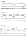
- first LOCOS oxide films 4 of about 400 nm thick are formed as device isolation films on a silicon substrate 1. Ion implantation is then performed to form a p-well region 2 and an n-well region 3.
- a silicon oxide film 5 of about 10 nm thick and a silicon nitride film 6 of about 100 nm thick are formed as shown in Fig. 1(b).
- the silicon nitride film 6 is patterned by photolithography and etching so that openings are formed above desired regions of the silicon substrate 1 between the first LOCOS oxide films 4.
- second LOCOS oxide films 7 are provided.
- the second LOCOS oxide film 7 is formed thinner than the first LOCOS oxide film 4.
- level difference between a source/drain region and a channel region to be formed in a later step is determined. At this stage, the thickness of the second LOCOS oxide film 7 is set to about 200 nm so that the level difference will finally be about 100 nm.
- the second LOCOS oxide films 7 are anisotropically etched until the silicon substrate 1 is exposed.
- the thus exposed surface of the silicon substrate 1 will serve as channel region 8 in a later step.
- bird's beaks 9 at both sides of the second LOCOS oxide films 7 are not etched away and remain there.
- the channel regions 8 are sacrificially oxidized and then a sacrificial oxide film is removed by wet etching with a HF solution in order to remove damages caused by the etching.
- gate insulating films 10 of about 4.5 nm thick are formed on the channel regions 8 by thermal oxidation.
- a polysilicon layer of about 400 nm thick is deposited on the entire surface of the silicon substrate 1 where the silicon nitride film 6 has been formed and etched back until the polysilicon layer on the silicon nitride film 6 is completely removed.
- gate electrodes 11 of about 200 nm thick are buried in the channel regions 8 without performing alignment for forming the gate electrodes.
- ion implantation of impurities is performed to the p-well region 2 and the n-well region 3, respectively using the gate electrodes 11 and the bird's beaks 9 as a mask and thermal treatment is performed under nitrogen atmosphere at 850°C to form source/drain regions 12 as shown in Fig. 1(e).
- the impurities are not implanted immediately below the bird's beaks 9.
- a cobalt film of about 20 nm thick is formed by sputtering on the entire surface of the silicon substrate 1 and thermally treated to form cobalt silicide films 13 of about 30 nm thick on the gate electrodes 11 and the source/drain regions 12 as shown in Fig. 1(f). Thereafter, unreacted cobalt film is removed.
- anisotropic etching is performed to the entire surface to remove the bird's beaks 9 as shown in Fig. 1(g) on conditions that the silicide films 13 will not be etched.
- impurities are implanted at low concentration to form LDD regions 14 as shown in Fig. 1(g).
- a silicon oxide film 15 of about 800 nm thick is formed by CVD on the silicon substrate 1. Then, contact holes are formed in the silicon oxide film 15 by photolithography and etching and wiring layers 16 are formed. Thus, the semiconductor device is completed as shown in Fig. 1(h).
- the silicide films 13 are provided on the surfaces of the gate electrodes 11 and the source/drain regions 12. Further, the surfaces of the LDD regions 14 are partially tapered and an interface between the source/drain region 12 and the silicide film 13 can be located higher than the surface of the semiconductor substrate immediately below the gate electrode 11. Accordingly, the source/drain region 12 can surely be formed thicker to some extent than the channel region 8. Therefore, leak current due to the silicide film 13 is prevented, which allows obtaining a highly reliable semiconductor device.
- the LDD region 14 is formed after the thermal treatment at 850°C for forming the source/drain region 12, undesired diffusion of impurities in the LDD region 14 in a lateral direction can be prevented, which ensures inhibition of short channel effect.
- the LDD region 14 can be formed while using the bird's beak 9 as a mask, an extra step of forming sidewall spacers commonly used for forming the LDD region can be omitted, which allows simplification of the manufacturing steps.
- the silicide film 13 since the bird's beak 9 covers almost completely the sidewalls of the gate electrode 11, the silicide film 13 is not formed between the gate electrode 11 and the source/drain region 12, so that short circuit therebetween is prevented.
- the source/drain region since the source/drain region has an LDD region whose surface is partially or entirely tapered and an interface between the semiconductor substrate and the silicide film in the source/drain region is located higher than a surface of the semiconductor substrate below the gate electrode, electric field concentration and short channel effect are inhibited by the LDD region. Further, the source/drain region is provided with the silicide film formed on its surface and has a sufficient thickness as compared with the channel region, which allows prevention of increase in leak current at a PN junction. Thus, a highly reliable semiconductor device can be obtained.
- a LOCOS oxide film is formed on a semiconductor substrate; the LOCOS oxide film is partially removed to form a recess on the semiconductor substrate; a gate electrode is buried in the recess through the intervention of a gate insulating film; ion implantation is performed using the gate electrode and the remaining LOCOS oxide film as a mask to form a source/drain region; a silicide film is formed at least on a surface of the source/drain region; and an LDD region is formed in the semiconductor substrate below both sides of the gate electrode.
- the gate electrode can be formed in self-alignment into the recess formed on the surface of the semiconductor substrate and variation in gate length is inhibited.
- the source/drain region can be formed to have a sufficient thickness as compared with the channel region, the silicide film is prevented from approaching the PN junction in the source/drain region and increase in leak current at the PN junction is inhibited.
- the step of forming the sidewall spacers is omitted and the short circuit between the gate electrode and the source/drain region can surely be prevented. Accordingly the manufacturing steps are simplified.
- the LDD region is formed after the formation of the source/drain region and the silicide film, the LDD region is not subjected to other thermal treatments than that performed for forming the LDD region, which inhibits lateral diffusion of low concentration impurities in the LDD region.
- the LDD region is not subjected to other thermal treatments than that performed for forming the LDD region, which inhibits lateral diffusion of low concentration impurities in the LDD region.
- the formation of the LDD region is carried out more suitably and conveniently, which allows simplification of the manufacturing steps and reduction of manufacturing costs.
Landscapes
- Insulated Gate Type Field-Effect Transistor (AREA)
- Electrodes Of Semiconductors (AREA)
- Metal-Oxide And Bipolar Metal-Oxide Semiconductor Integrated Circuits (AREA)
Abstract
Description
Claims (10)
- A semiconductor device comprising: a gate electrode formed on a semiconductor substrate through the intervention of a gate insulating film; and a source/drain region provided with a silicide film on its surface and formed in the semiconductor substrate,
wherein the source/drain region has an LDD region whose surface is partially or entirely tapered and an interface between the semiconductor substrate and the silicide film in the source/drain region is located higher than a surface of the semiconductor substrate below the gate electrode. - A semiconductor device according to claim 1, wherein the surface of the gate electrode is located higher than the surface of the semiconductor substrate where the recess is not provided.
- A semiconductor device according to claim 1, wherein the LDD region is partially or entirely inclined with respect to the surface of the semiconductor substrate where the recess is not provided, and the LDD region is formed on an inclined surface of the semiconductor substrate, in the flat semiconductor substrate to have inclination by itself or in the inclined semiconductor substrate to have inclination by itself.
- A semiconductor device according to claim 3, wherein the LDD region is formed on an inclined surface of the semiconductor substrate.
- A semiconductor device according to claim 1, wherein the thickness of the LOCOS oxide film is 100 to 300 nm.
- A process of manufacturing a semiconductor device comprising the steps of:forming a LOCOS oxide film on a semiconductor substrate;partially removing the LOCOS oxide film to form a recess on the semiconductor substrate;burying a gate electrode in the recess through the intervention of a gate insulating film;performing ion implantation using the gate electrode and the remaining LOCOS oxide film as a mask to form a source/drain region;forming a silicide film at least on a surface of the source/drain region; andforming an LDD region in the semiconductor device below both sides of the gate electrode.
- A process according to claim 6, wherein the LOCOS oxide film is formed utilizing a mask for formation of the LOCOS oxide film and the LOCOS oxide film is partially removed using the mask for formation of the LOCOS oxide film.
- A process according to claim 7, wherein the LOCOS oxide film is removed by anisotropic etching so that a bird's beak remains partially or entirely.
- A process according to claim 6, wherein the remaining LOCOS oxide film is removed after the formation of the silicide film before the formation of the LDD region.
- A semiconductor device according to claim 6, wherein the thickness of the LOCOS oxide film is 100 to 300 nm.
Applications Claiming Priority (2)
| Application Number | Priority Date | Filing Date | Title |
|---|---|---|---|
| JP2000133752A JP3490046B2 (en) | 2000-05-02 | 2000-05-02 | Semiconductor device and manufacturing method thereof |
| JP2000133752 | 2000-05-02 |
Publications (3)
| Publication Number | Publication Date |
|---|---|
| EP1152470A2 true EP1152470A2 (en) | 2001-11-07 |
| EP1152470A3 EP1152470A3 (en) | 2004-02-25 |
| EP1152470B1 EP1152470B1 (en) | 2008-01-02 |
Family
ID=18642172
Family Applications (1)
| Application Number | Title | Priority Date | Filing Date |
|---|---|---|---|
| EP01304019A Expired - Lifetime EP1152470B1 (en) | 2000-05-02 | 2001-05-02 | Semiconductor device with LDD structure and process of manufacturing the same |
Country Status (6)
| Country | Link |
|---|---|
| US (1) | US6492696B2 (en) |
| EP (1) | EP1152470B1 (en) |
| JP (1) | JP3490046B2 (en) |
| KR (1) | KR100393139B1 (en) |
| DE (1) | DE60132129T2 (en) |
| TW (1) | TW508825B (en) |
Families Citing this family (14)
| Publication number | Priority date | Publication date | Assignee | Title |
|---|---|---|---|---|
| KR100355034B1 (en) * | 1999-07-15 | 2002-10-05 | 삼성전자 주식회사 | Semiconductor device with SEG layer and Method for isolating thereof |
| US6573143B1 (en) * | 2001-11-28 | 2003-06-03 | Chartered Semiconductor Manufacturing Ltd. | Trench transistor structure and formation method |
| US6677646B2 (en) * | 2002-04-05 | 2004-01-13 | International Business Machines Corporation | Method and structure of a disposable reversed spacer process for high performance recessed channel CMOS |
| US7494894B2 (en) * | 2002-08-29 | 2009-02-24 | Micron Technology, Inc. | Protection in integrated circuits |
| US6930030B2 (en) * | 2003-06-03 | 2005-08-16 | International Business Machines Corporation | Method of forming an electronic device on a recess in the surface of a thin film of silicon etched to a precise thickness |
| KR100597459B1 (en) * | 2003-12-31 | 2006-07-05 | 동부일렉트로닉스 주식회사 | Gate electrode formation method of semiconductor device |
| JP4945900B2 (en) * | 2005-01-06 | 2012-06-06 | ソニー株式会社 | Insulated gate field effect transistor and manufacturing method thereof |
| KR100668856B1 (en) * | 2005-06-30 | 2007-01-16 | 주식회사 하이닉스반도체 | Manufacturing method of semiconductor device |
| US8258057B2 (en) * | 2006-03-30 | 2012-09-04 | Intel Corporation | Copper-filled trench contact for transistor performance improvement |
| KR100842483B1 (en) * | 2006-12-28 | 2008-07-01 | 동부일렉트로닉스 주식회사 | Manufacturing Method of Semiconductor Device |
| FR2995135B1 (en) * | 2012-09-05 | 2015-12-04 | Commissariat Energie Atomique | METHOD FOR PRODUCING FET TRANSISTORS |
| CN109300789B (en) * | 2017-07-25 | 2021-07-09 | 中芯国际集成电路制造(上海)有限公司 | Semiconductor structure and method of forming the same |
| US10910313B2 (en) | 2017-11-16 | 2021-02-02 | Samsung Electronics Co., Ltd. | Integrated circuit including field effect transistors having a contact on active gate compatible with a small cell area having a small contacted poly pitch |
| US10861950B2 (en) | 2017-11-16 | 2020-12-08 | Samsung Electronics Co., Ltd. | Integrated circuit including field effect transistors having a contact on active gate compatible with a small cell area having a small contacted poly pitch |
Family Cites Families (16)
| Publication number | Priority date | Publication date | Assignee | Title |
|---|---|---|---|---|
| JPH05152320A (en) * | 1991-11-30 | 1993-06-18 | Ricoh Co Ltd | LDD structure semiconductor device and method of manufacturing the same |
| US5567966A (en) * | 1993-09-29 | 1996-10-22 | Texas Instruments Incorporated | Local thinning of channel region for ultra-thin film SOI MOSFET with elevated source/drain |
| KR950021242A (en) * | 1993-12-28 | 1995-07-26 | 김광호 | Polycrystalline Silicon Thin Film Transistor and Manufacturing Method Thereof |
| JP2906971B2 (en) * | 1993-12-30 | 1999-06-21 | 日本電気株式会社 | Method for manufacturing semiconductor memory device |
| KR0162673B1 (en) * | 1994-01-11 | 1998-12-01 | 문정환 | Manufacture of conducting layer and semiconductor device |
| US5529942A (en) * | 1994-06-23 | 1996-06-25 | United Microelectronics Corp. | Self-aligned coding process for mask ROM |
| JPH08148561A (en) * | 1994-11-16 | 1996-06-07 | Mitsubishi Electric Corp | Semiconductor device and manufacturing method thereof |
| US5656519A (en) * | 1995-02-14 | 1997-08-12 | Nec Corporation | Method for manufacturing salicide semiconductor device |
| US5672524A (en) * | 1995-08-01 | 1997-09-30 | Advanced Micro Devices, Inc. | Three-dimensional complementary field effect transistor process |
| JPH0992728A (en) * | 1995-09-21 | 1997-04-04 | Mitsubishi Electric Corp | Complementary MOS field effect transistor and manufacturing method thereof |
| JP3734559B2 (en) * | 1996-03-15 | 2006-01-11 | 富士通株式会社 | Manufacturing method of semiconductor device |
| JPH1092949A (en) | 1996-09-10 | 1998-04-10 | Hitachi Ltd | Semiconductor integrated circuit device and method of manufacturing the same |
| JP3382840B2 (en) * | 1997-05-23 | 2003-03-04 | シャープ株式会社 | Method for manufacturing semiconductor device |
| JPH11154749A (en) | 1997-09-22 | 1999-06-08 | Nippon Steel Corp | Semiconductor device and manufacturing method thereof |
| KR100314708B1 (en) * | 1998-07-03 | 2002-04-24 | 윤종용 | Manufacturing Method of Semiconductor Device with Built-in Pyrom Cell |
| US6261909B1 (en) * | 1999-01-05 | 2001-07-17 | Advanced Micron Devices, Inc. | Semiconductor device having ultra shallow junctions and a reduced channel length and method for making same |
-
2000
- 2000-05-02 JP JP2000133752A patent/JP3490046B2/en not_active Expired - Fee Related
-
2001
- 2001-04-25 KR KR10-2001-0022279A patent/KR100393139B1/en not_active Expired - Fee Related
- 2001-05-02 TW TW090110505A patent/TW508825B/en not_active IP Right Cessation
- 2001-05-02 US US09/846,391 patent/US6492696B2/en not_active Expired - Fee Related
- 2001-05-02 EP EP01304019A patent/EP1152470B1/en not_active Expired - Lifetime
- 2001-05-02 DE DE60132129T patent/DE60132129T2/en not_active Expired - Fee Related
Also Published As
| Publication number | Publication date |
|---|---|
| JP3490046B2 (en) | 2004-01-26 |
| US20010039092A1 (en) | 2001-11-08 |
| US6492696B2 (en) | 2002-12-10 |
| JP2001320044A (en) | 2001-11-16 |
| DE60132129T2 (en) | 2008-12-11 |
| EP1152470A3 (en) | 2004-02-25 |
| KR20010100915A (en) | 2001-11-14 |
| KR100393139B1 (en) | 2003-07-31 |
| TW508825B (en) | 2002-11-01 |
| DE60132129D1 (en) | 2008-02-14 |
| EP1152470B1 (en) | 2008-01-02 |
Similar Documents
| Publication | Publication Date | Title |
|---|---|---|
| US6232641B1 (en) | Semiconductor apparatus having elevated source and drain structure and manufacturing method therefor | |
| US5885861A (en) | Reduction of dopant diffusion by the co-implantation of impurities into the transistor gate conductor | |
| US6987291B2 (en) | Integrated transistor circuitry | |
| US7288470B2 (en) | Semiconductor device comprising buried channel region and method for manufacturing the same | |
| US6737308B2 (en) | Semiconductor device having LDD-type source/drain regions and fabrication method thereof | |
| US5683924A (en) | Method of forming raised source/drain regions in a integrated circuit | |
| US5714393A (en) | Diode-connected semiconductor device and method of manufacture | |
| EP1211716A2 (en) | Semiconductor device and fabrication process therefor using a dummy gate | |
| JP2000243958A (en) | Semiconductor device and manufacturing method thereof | |
| US6492696B2 (en) | Semiconductor device and process of manufacturing the same | |
| JPH118387A (en) | Semiconductor device and manufacturing method thereof | |
| US5888873A (en) | Method of manufacturing short channel MOS devices | |
| US6847086B2 (en) | Semiconductor device and method of forming the same | |
| JP2000082808A (en) | Semiconductor device and manufacturing method thereof | |
| US6395606B1 (en) | MOSFET with metal in gate for reduced gate resistance | |
| US20090162980A1 (en) | Method of manufacturing semiconductor device | |
| US6063676A (en) | Mosfet with raised source and drain regions | |
| JP2000049348A (en) | Semiconductor device having elevated source / drain structure and method of manufacturing the same | |
| US7521767B2 (en) | MOS transistor in a semiconductor device | |
| EP0851486A1 (en) | A process for manufacturing a semiconductor device | |
| EP0967637A1 (en) | Semiconductor device and manufacturing method | |
| JPH0786586A (en) | Semiconductor device and manufacturing method thereof | |
| JP4159197B2 (en) | Manufacturing method of semiconductor device | |
| JPH08130310A (en) | MOS device and method of manufacturing the same |
Legal Events
| Date | Code | Title | Description |
|---|---|---|---|
| PUAI | Public reference made under article 153(3) epc to a published international application that has entered the european phase |
Free format text: ORIGINAL CODE: 0009012 |
|
| AK | Designated contracting states |
Kind code of ref document: A2 Designated state(s): AT BE CH CY DE DK ES FI FR GB GR IE IT LI LU MC NL PT SE TR |
|
| AX | Request for extension of the european patent |
Free format text: AL;LT;LV;MK;RO;SI |
|
| RIC1 | Information provided on ipc code assigned before grant |
Ipc: 7H 01L 21/762 B Ipc: 7H 01L 21/336 B Ipc: 7H 01L 21/8238 B Ipc: 7H 01L 29/417 B Ipc: 7H 01L 29/08 A |
|
| PUAL | Search report despatched |
Free format text: ORIGINAL CODE: 0009013 |
|
| AK | Designated contracting states |
Kind code of ref document: A3 Designated state(s): AT BE CH CY DE DK ES FI FR GB GR IE IT LI LU MC NL PT SE TR |
|
| AX | Request for extension of the european patent |
Extension state: AL LT LV MK RO SI |
|
| 17P | Request for examination filed |
Effective date: 20040812 |
|
| AKX | Designation fees paid |
Designated state(s): DE FR GB NL |
|
| GRAP | Despatch of communication of intention to grant a patent |
Free format text: ORIGINAL CODE: EPIDOSNIGR1 |
|
| GRAS | Grant fee paid |
Free format text: ORIGINAL CODE: EPIDOSNIGR3 |
|
| GRAA | (expected) grant |
Free format text: ORIGINAL CODE: 0009210 |
|
| AK | Designated contracting states |
Kind code of ref document: B1 Designated state(s): DE FR GB NL |
|
| REG | Reference to a national code |
Ref country code: GB Ref legal event code: FG4D |
|
| REF | Corresponds to: |
Ref document number: 60132129 Country of ref document: DE Date of ref document: 20080214 Kind code of ref document: P |
|
| PGFP | Annual fee paid to national office [announced via postgrant information from national office to epo] |
Ref country code: DE Payment date: 20080529 Year of fee payment: 8 |
|
| ET | Fr: translation filed | ||
| PGFP | Annual fee paid to national office [announced via postgrant information from national office to epo] |
Ref country code: NL Payment date: 20080531 Year of fee payment: 8 |
|
| PLBE | No opposition filed within time limit |
Free format text: ORIGINAL CODE: 0009261 |
|
| STAA | Information on the status of an ep patent application or granted ep patent |
Free format text: STATUS: NO OPPOSITION FILED WITHIN TIME LIMIT |
|
| 26N | No opposition filed |
Effective date: 20081003 |
|
| PGFP | Annual fee paid to national office [announced via postgrant information from national office to epo] |
Ref country code: GB Payment date: 20080507 Year of fee payment: 8 |
|
| GBPC | Gb: european patent ceased through non-payment of renewal fee |
Effective date: 20090502 |
|
| NLV4 | Nl: lapsed or anulled due to non-payment of the annual fee |
Effective date: 20091201 |
|
| PG25 | Lapsed in a contracting state [announced via postgrant information from national office to epo] |
Ref country code: NL Free format text: LAPSE BECAUSE OF NON-PAYMENT OF DUE FEES Effective date: 20091201 |
|
| REG | Reference to a national code |
Ref country code: FR Ref legal event code: ST Effective date: 20100129 |
|
| PG25 | Lapsed in a contracting state [announced via postgrant information from national office to epo] |
Ref country code: FR Free format text: LAPSE BECAUSE OF NON-PAYMENT OF DUE FEES Effective date: 20090602 |
|
| PGFP | Annual fee paid to national office [announced via postgrant information from national office to epo] |
Ref country code: FR Payment date: 20080429 Year of fee payment: 8 |
|
| PG25 | Lapsed in a contracting state [announced via postgrant information from national office to epo] |
Ref country code: GB Free format text: LAPSE BECAUSE OF NON-PAYMENT OF DUE FEES Effective date: 20090502 |
|
| PG25 | Lapsed in a contracting state [announced via postgrant information from national office to epo] |
Ref country code: DE Free format text: LAPSE BECAUSE OF NON-PAYMENT OF DUE FEES Effective date: 20091201 |