EP1152468A2 - Application specific integrated circuit with spaced spare logic gate subgroups and method of fabrication - Google Patents
Application specific integrated circuit with spaced spare logic gate subgroups and method of fabrication Download PDFInfo
- Publication number
- EP1152468A2 EP1152468A2 EP01108614A EP01108614A EP1152468A2 EP 1152468 A2 EP1152468 A2 EP 1152468A2 EP 01108614 A EP01108614 A EP 01108614A EP 01108614 A EP01108614 A EP 01108614A EP 1152468 A2 EP1152468 A2 EP 1152468A2
- Authority
- EP
- European Patent Office
- Prior art keywords
- spare
- operational
- subgroup
- logic gates
- metal layer
- Prior art date
- Legal status (The legal status is an assumption and is not a legal conclusion. Google has not performed a legal analysis and makes no representation as to the accuracy of the status listed.)
- Withdrawn
Links
Images


Classifications
-
- G—PHYSICS
- G06—COMPUTING OR CALCULATING; COUNTING
- G06F—ELECTRIC DIGITAL DATA PROCESSING
- G06F30/00—Computer-aided design [CAD]
- G06F30/30—Circuit design
-
- H—ELECTRICITY
- H10—SEMICONDUCTOR DEVICES; ELECTRIC SOLID-STATE DEVICES NOT OTHERWISE PROVIDED FOR
- H10D—INORGANIC ELECTRIC SEMICONDUCTOR DEVICES
- H10D84/00—Integrated devices formed in or on semiconductor substrates that comprise only semiconducting layers, e.g. on Si wafers or on GaAs-on-Si wafers
- H10D84/90—Masterslice integrated circuits
- H10D84/903—Masterslice integrated circuits comprising field effect technology
- H10D84/907—CMOS gate arrays
-
- H—ELECTRICITY
- H10—SEMICONDUCTOR DEVICES; ELECTRIC SOLID-STATE DEVICES NOT OTHERWISE PROVIDED FOR
- H10D—INORGANIC ELECTRIC SEMICONDUCTOR DEVICES
- H10D89/00—Aspects of integrated devices not covered by groups H10D84/00 - H10D88/00
- H10D89/10—Integrated device layouts
Definitions
- the present invention relates to application specific integrated circuits (ASIC). More particularly, it relates to an ASIC, especially a multiple metal layer ASIC, having easily accessible spare gate wiring.
- ASIC application specific integrated circuits
- An application specific integrated circuit is a microelectronic integrated circuit chip designed specifically for an application or product, such as a computer system.
- the ASIC forms, in a single, semi-conductor substrate, the equivalent of several different integrated circuits each designed to perform one or more desired operations, such as a microprocessor operation, a memory operation, various interface operations (e.g., memory interface, processor interface), etc. Effectively, then, the ASIC is definable by one or more operational zones or "blocks" each having desired operational capabilities.
- ASIC operational blocks are typically designed to include thousands of individual logic gates necessary for performing the desired operation(s). These logic gates (or “operational logic gates”) are formed in a substrate layer according to known semi-conductor fabrication techniques. The operational logic gates can assume a wide variety of forms, and include varying circuitry configurations. Once formed, the various operational logic gates are subsequently interconnected by wiring routed into metal layer(s) formed on top of the substrate. So as to optimize operational block size, the various operational logic gates associated with a particular operational block are located in relative close proximity to one another. By densely packaging the operational logic gates, the length of the interconnecting wiring including individual wiring "runs", is minimized.
- all of the operational logic gates of a particular block are formed within a relatively small area, thereby defining a boundary within which all of the operational logic gates are located.
- the boundary associated with a particular operational block does not physically appear on the chip, but instead exists in the abstract.
- the operational block may not perform desired operation(s), logic "bugs" may be identified, logic changes required, one or more of the logic gates or wiring may be defective, etc. Rather than scrap the entire chip, repairs are typically performed to correct the identified problem.
- a widely employed technique for facilitating ASIC repair is to randomly dispense a number of spare logic gates throughout the operational block.
- a variety of different logic gates, such as AND gates, OR gates, NAND gates, NOR gates, invertors, flip-flops, and registers, are typically provided.
- the spare logic gates are, similar to the operational logic gates, wired to one another via the metal layer(s).
- one or more the spare logic gates able to correct the problem can be identified and incorporated into the operational logic gate circuitry. As there are already wires between the spare logic gates, it is likely that there will be points along those wires from which the desired spare logic gate(s) can be wired into the functional chip logic.
- FIB focused ion beam
- the FIB technique can be used as an aide in integrated circuit design and debug by performing rapid device alteration.
- a beam of Ga ions is focused and scanned over the surface of the chip.
- the interaction of the ion beam with the sample results in ejection of atoms from the surface (sputtering) is used to expose buried wiring lines for eventually cutting/attaching to other circuit elements.
- the holes and cuts can be very accurately placed (within about 0.1 ⁇ m) and can reach buried layers.
- FIB can be implemented to deposit a metal layer or wire when performed in the presence of an organometallic gas. This formed metal layer or wire, in turn, can be used to make connections from one device to another.
- FIB repair technique While the FIB repair technique is highly viable, certain limitations have been identified.
- ASIC technology has evolved to require the use of multiple metal layers over the semi-conductor substrate layer.
- current chip designs incorporate six metal layers.
- the wiring connecting the various operational logic gates, as well as the spare logic gates, is formed along one or more of these metal layers.
- an automatic routing tool determines and routes individual wires as each successive metal layer is formed. Statistically speaking, it is highly likely that the automatic routing tool will route or place the interconnecting wire for closely positioned logic gates along one of the inner most metal layers.
- the FIB can access wiring located on the outer most metal layer, as well as the metal layer directly beneath the outer most layer.
- FIB may be able to access intermediate metal layers.
- the FIB cannot reach inner metal layers, such as those formed beneath four or more metal layers.
- FIB technology can only reach wires in the top few metal layers of an ASIC. Where six or more metal layers are employed, spare logic gates connected by wiring formed on the inner most metal layers are essentially useless as the wiring is not accessible by FIB.
- ASIC integrated circuit technology continues to evolve and improve.
- the complexity of ASIC designs has increased exponentially, as well as the fabrication of these chips.
- the availability of spare logic gates to address unforeseen logic/performance problems remains a necessity.
- currently employed ASIC operational block design techniques may render the spare logic gates unusable, especially for multiple metal layer designs. Therefore, a need exists for an ASIC operational block design including spare logic gates strategically located to ensure accessibility by a repair tool, and a method for ensuring this desired configuration.
- the resulting ASIC would be highly useful for a number of devices, including computer systems.
- the ASIC includes a substrate layer, at least one metal layer and an operational block.
- the metal layer is formed above the substrate layer.
- the operational block is formed in the substrate layer and the metal layer, and is definable by a two-dimensional boundary.
- the operational block includes a plurality of operational logic gates, a first subgroup of spare logic gates, a second subgroup of spare logic gates, operational wiring and spare gate wiring.
- the operational logic gates and the spare logic gates are formed in the substrate layer, positioned within the boundary. Further, the first subgroup is spaced from the second subgroup.
- the operational wiring is formed in the metal layer and interconnects the operational logic gates to configure the operational block to perform a desired operation.
- the spare gate wiring is formed in the metal layer.
- the spare gate wiring is separate from the operational wiring, and connects at least one of the first subgroup spare gates to at least one of the second subgroup spare logic gates.
- the operational block boundary defines a major dimension, and a spacing between the first and second subgroups is at least one-half the major dimension.
- the ASIC includes first, second, third, fourth, fifth, and sixth metal layers sequentially formed above the substrate layer such that the first metal layer is an inner metal layer, proximal the substrate layer. With this configuration, at least a portion of the spare gate wiring extends to the fifth metal layer.
- the ASIC is designed to perform desired operations of the custom computer system, such as processing and/or memory operations.
- the ASIC includes a substrate layer, at least one metal layer and an operational block.
- the metal layer is formed above the substrate layer.
- the operational block is formed in the substrate layer and the metal layer, and is definable by a two-dimensional boundary.
- the operational block further includes a plurality of operational logic gates, a first subgroup of spare logic gates, a second subgroup of spare logic gates, operational wiring and spare gate wiring. These subgroups are spaced from one another within the boundary.
- the operational wiring is formed in the metal layer and interconnects the operational logic gates to configure the operational block to perform a desired operation of the custom computer system.
- the spare gate wiring is formed in the metal layer.
- the spare gate wiring is separate from the operational wiring and connects at least one of the first subgroup spare gates to at least one of the second subgroup spare logic gates.
- the ASIC includes a plurality of metal layers, and a spacing between the subgroups dictates that at least a portion of the spare gate wiring extends to one of the outer metal layers.
- the operational block includes operational logic gates for performing a desired operation.
- the method includes assigning spare logic gates to one of a first subgroup and a second subgroup.
- An abstract, two-dimensional boundary is defined for the operational block.
- a substrate layer is provided.
- the operational logic gates are formed on the substrate layer.
- the first and second subgroups are formed on the substrate layer such that each of the subgroups are spaced from one another within the boundary.
- a metal layer is formed over the substrate layer.
- Operational wiring is routed in the metal layer interconnecting the operational logic gates. The operational wiring configures the operational block to perform the desired operation.
- spare gate wiring is routed into the metal layer, connecting at least one of the first subgroup spare gates to at least one of the second subgroup spare gates.
- a plurality of metal layers are formed over the substrate layer and the subgroups are spaced a sufficient distance to ensure extension of the spare gate wiring to one of the outer metal layers.
- One embodiment of the present invention is directed to an ASIC and a related method of manufacture.
- An ASIC 10 is illustrated generally in FIG. 1 as part of a wafer 12.
- the wafer 12 is typically fabricated to include a plurality of the ASICs 10.
- the ASIC 10 is shown in greater detail by the simplified plan view of FIG. 2.
- the ASIC 10 is an integrated circuit including one or more operational blocks 14.
- Each of the operational blocks 14 are depicted in FIG. 2 as having a discernable boundary or perimeter 16.
- the boundary 16 is not physically formed in the ASIC 10.
- each of the operational blocks 14 includes, as described in greater detail below, a vast number of operational gates that are densely packed into a small area. In accordance with accepted operational block layout parameters, the resulting logic gate placements result in the abstract, two-dimensional boundary 16.
- the operational blocks 14 are designed to provide the ASIC 10 with a number of different operational characteristics specific to the end application.
- the operational blocks 14 can be designed to serve as one or more of a processor, a memory, a processor interface, memory interface, etc.
- FIG. 3A provides a simplified top plan view of the operational block 14, whereas FIG. 3B is a simplified cross-sectional view of FIG. 3A.
- the operational block 14 includes a plurality of operational logic gates 20, a first subgroup 22 of spare logic gates and a second subgroup 24 of spare logic gates.
- the term "operational logic gate” is in reference to a logic gate designed to form part of the ASIC 10 functional logic, whereas a “spare logic gate” is not, at least initially, used.
- Each of the individual operational logic gates 20 can. assume a wide variety of known electronic configurations, such as an AND gate, OR gate, NAND gate, NOR gate, flip-flop, invertor, register, etc.
- the types and quantities of the operational logic gates 20 are specifically selected to produce a desired operation(s) for the operational block 14 once interconnected. As such, the number and location of the operational logic gates 20 will vary depending upon the particular design of the operational block 14 and can include thousands of individual logic gates. For ease of illustration, the relative size of the operational logic gates 20 has been greatly exaggerated.
- each of the subgroups 22, 24 includes a plurality of spare logic gates (several of which are shown generally at 26) selected in accordance with performance characteristics of the operational block 14 such as AND gates, OR gates, NAND gates, NOR gates, etc.
- the spare logic gates 26 are clustered or densely positioned within each of the respective subgroups 22, 24. As a point of reference, a maximum spacing between the individual spare logic gates 26 within a respective subgroup is on the order of 2 microns.
- each of the subgroups 22, 24 includes 20-50 spare logic gates, although any other number, either greater or smaller, is equally acceptable. Further, more than two of the subgroups 22,24 can be provided.
- the ASIC 10 onto which the operational block 14 is formed includes a substrate layer 30 and at least one metal layer 32.
- the substrate layer 30 is formed of an acceptable semiconductive material, preferably silicon or germanium.
- the metal layer 32 is formed from an appropriate metallic material, preferably copper or aluminum, above the substrate layer 30.
- a plurality of metal layers are provided.
- six metal layers 32a-32f are sequentially formed over the substrate layer 30.
- the first metal layer 32a is an inner most metal layer, proximal the substrate layer 30.
- the sixth metal layer 32f is an outer most layer, distal the substrate layer 30.
- any other number of metal layers 32 can be provided.
- additional metal layers can be formed over the sixth metal layer 32f.
- outer layers which encompasses the outer most two or three metal layers 32, such as, for example, the fifth and sixth metal layers 32e, 32f.
- inner layers which encompasses the inner most two or three metal layers 32, such as, for example, the first and second metal layers 32a, 32b.
- intermediate layers for example the third and fourth metal layers 32c, 32d.
- the metal layer(s) 32 provides a conductive surface through which the various logic gates are connected.
- This electrical connection is provided in the form of operational wiring 40 and spare gate wiring 42, each of which includes a series of individual wires routed into the metal layer(s) 32.
- the operational block 14 includes thousands of individual operational logic gates 20. Each of the operational logic gates 20 are interconnected by the operational wiring 40 to configure the operational block 14 to perform a desired operation.
- the operational wiring 40 consists of thousands of individual "wires" routed into the various metal layers 32.
- the operational logic gates 20a, 20b are electrically connected by the wire 40a
- the operational logic gates 20c, 20d are electrically connected by the wire 40b.
- routing of the operational wiring 40 is performed by an automatic routing tool (not shown).
- Each of the metal layers 32a-32f are available for wire routing runs.
- the automatic routing tool optimizes wiring density by limiting, as much as possible, the formation of wiring in the outer metal layers, such as the metal layers 32e, 32f. More particularly, for closely spaced operational logic gates 20, the automatic routing tool will limit the associated operational wiring 40 to the first or second metal layer 32a, 32b.
- layout of the operational logic gates 20 typically strives to place related operational logic gates in close proximity to one another. Thus, for example, the operational gates 20a, 20b are located in close proximity to one another.
- the associated operational wire 40a extends only to the first metal layer 30a.
- the operational logic gates 20c, 20d are separated slightly from one another.
- the associated operational wire 40b extends along the first metal layer 32a and the second metal layer 32b.
- the spare logic gates 26 comprising the first and second subgroups 22, 24 are similarly electrically connected to one another by the spare gate wiring 42 (shown generally in FIGS. 3A and 3B).
- the spare gate wiring 42 preferably includes a number of individually routed wires.
- one of the spare logic gates (referenced as 26a) of the first subgroup 22 is connected to a respective one of the spare logic gates (referenced as 26b) of the second subgroup 24 by an individual wire (referenced as 42a).
- the individual spare logic gates 26 comprising each of the first and second subgroups 22, 24 are selected and connected in accordance with possible repair requirements of the operational block 14.
- the spare gate wiring 42 is formed or routed by an automatic routing tool.
- the first and second subgroups 22, 24 are formed on the substrate layer 30 so as to be spaced from one another, thereby ensuring that the spare gate wiring 42 extends to the outer metal layers, such as the metal layers 32e, 32f.
- a desired spacing of the subgroups 22, 24 is best described with respect to dimensions provided by the boundary 16.
- the boundary 16 can be described as defining a major dimension X and a minor dimension Y.
- a spacing or distance between the subgroups 22, 24 is at least one-half the major dimension X; most preferably at least two-thirds the major dimension X.
- the boundary 16 has a major dimension of approximately 4 mm and a minor dimension of approximately 1 mm.
- the subgroups 22, 24 are spaced by approximately 2-3 mm.
- the subgroups 22, 24 are preferably centered relative to the minor dimension Y.
- FIG. 3A provides a simplified, plan view of an alternative operational block 50 including the first subgroup 22 and the second subgroup 24.
- the subgroups 22, 24 need not be centered relative to the boundary 16; however, the desired spacing between subgroups 22, 24 is still provided.
- the spacing between subgroups 22, 24 dictates that the spare gate wiring 42 extends beyond the inner metal layer(s), such as the first and second layers 32a, 32b, to the outer layer(s), such as the fifth layer 32e.
- the automated routing tool utilizes certain algorithms to determine placement/extension of the spare gate wiring 42.
- the automatic routing tool is effectively "forced" to route the spare gate wiring 42 into the outer metal layers, such as the layers 32e, 32f.
- each of the subgroups 22, 24 includes a number of individual spare logic gates and that the spare gate wiring 42 includes a number of individual wires, such as the wire 42a, extending between the subgroups 22, 24.
- each of the individual spare gate wires extends to the outer metal layers, such as one of the metal layers 32e,32f.
- a FIB tool (not shown) can access the spare gate wiring 42 at the outer metal layer(s).
- the FIB can consistently pass through, and therefore access, wiring formed in the fifth and sixth metal layers 32e, 32f. Further, the FIB may be able to access the third and fourth metal layers 32c, 32d.
- the FIB due to inherent FIB limitations, as well as wiring density, it is likely impossible for the FIB to access wiring formed in the first and second metal layers 32a, 32b. Therefore, by routing at least a portion of the spare gate wiring 42 along the outer metal layers, such as the fifth or sixth metal layers 32e, 32f, the availability of the spare logic gates 26 associated with the spare gate wiring 42 is ensured.
- One embodiment of the method of manufacturing the ASIC 10, and in particular, the operational block 14, is illustrated generally at 60 in flow diagram form in FIG. 4.
- desired operating parameters or functions of the ASIC 10 are defined.
- the desired functions are application specific.
- the defined functions can include processing, memory, etc.
- a wide variety of functions are available.
- the operational block(s) 14 comprising the ASIC 10 is designed.
- the basic operational block 14 design is based upon the defined ASIC functions.
- a plurality of operational blocks 14 can be designed, each configured to have one or more operational characteristics.
- design of the operational block 14 includes the types and quantities of the operational logic gates 20 necessary for configuring the operational block 14 to perform the desired operation(s).
- design of the operational block 14 includes determining types and quantities of spare logic gates 26. As is known in the art, the types and quantities of spare logic gates correlates with the selected operational logic gates.
- the boundary 16 of the operational block 14 is determined.
- the boundary 16 is an abstract, two-dimensional feature, the size or parameters of which are based upon the previously selected operational logic gates 20.
- the selected spare logic gates are assigned to at least one of the first subgroup 22 and the second subgroup 24.
- the spare logic gates can be randomly assigned.
- the spare logic gates 26 can be specifically assigned based upon circuitry/logic characteristics.
- a minimum spacing between the subgroups 22, 24 is established. In one preferred embodiment, this minimum spacing is based upon dimensions defined by the operational block boundary 16. As previously described, the abstract boundary 16 is definable by a major dimension (such as the major dimension X in FIG. 3A). The minimum spacing established at step 70 is preferably formulated as a function of this major dimension X; for example, a minimum spacing of at least one-half the major dimension X, more preferably at least two-thirds the major dimension X.
- specific locations of the subgroups 22, 24 relative to the boundary 16 can be defined. For example, a specific location of the first subgroup 22 relative to the boundary 16 can be specified, for example centered relative to the minor dimension (such as the minor dimension Y of FIG.
- the second subgroup 24 can be spaced from the first subgroup 22 by distance of two-thirds the major dimension X.
- the substrate layer 30 is provided.
- the operational logic gates 20 are formed on the substrate layer 30 at step 74.
- the operational logic gates 20 are formed by an automatic gate placement tool.
- the gate placement tool locates each of the operational gates 20 within the boundary 16, positioning associated gates in close proximity to one another.
- each of the first and second subgroups 22, 24 includes a plurality of spare logic gates 26. Similar to the operational logic gates 20, the spare logic gates 26 are formed by an automatic gate placement tool. As such, the spare logic gates 26, and thus the first and second subgroups 22, 24, can be formed simultaneously with the operational logic gates 20, or before or after the operational logic gates 20 are positioned. Regardless, each of the first and second subgroups 22, 24 are formed to include a plurality of clustered spare logic gates, preferably in the range of approximately 20-50 spare logic gates. Further, the subgroups 22, 24 are spaced within the boundary 16 in accordance with the minimum spacing requirements established at step 70. In one preferred embodiment, the automated gate placement tool is provided with programming instructions relating to either the established minimum spacing between the subgroups 22, 24, or specific locations of the subgroups 22, 24.
- one or more of the metal layers 32 are formed on the substrate layer 30.
- six of the metal layers 32a-32f are sequentially formed over the substrate layer 30.
- any other number of metal layers 32 is acceptable.
- the metal layer(s) 32 is routed to form the operational wiring 40 that interconnects the operational logic gates 20.
- an automatic routing tool (not shown) is utilized to route the metal layer(s) 32.
- each metal layer 32 is routed to form a portion, or an entirety, of each individual operational wire prior to formation of the successive metal layer 32.
- the first metal layer 32a is routed with the wire 40a prior to placement of the second metal layer 32b.
- the first metal layer 32a is routed to form a portion of the wire 40b prior to the formation of the second metal layer 32b.
- the second metal layer 32b is routed to complete the wire 40b prior to placement of the third metal layer 32c.
- the operational wiring 40 configures the operational logic gates 20, and thus, the operational block 14, to perform the desired operation(s).
- the metal layer(s) 32 is routed to form the spare gate wiring 42 connecting at least one of the spare logic gates 26 of the first subgroup 22 to at least one of the spare logic gates 26 of the second subgroup 24.
- the spare gate wiring 42 includes a plurality of individual wires electrically connecting each of the subgroup 22, 24 spare logic gates, respectively. Similar to the operational wiring 40, the spare gate wiring 42 is preferably formed or routed in the metal layer(s) 32 by an automatic routing tool. In this regard, where a plurality of metal layers 32 are provided, the spacing between the subgroups 22, 24 dictates or "forces" the automatic routing tool to extend the spare gate wiring 42 along the outer metal layers (for example, the metal layers 32e of FIG. 3B).
- the automatic routing tool will, based upon internal algorithms, make the long runs along the outer metal layers 32. Notably, no specific routing instructions or programming are required. As previously described, each metal layer 32 is routed with a portion of the spare gate wiring 42 prior to formation of a successive metal layer 32.
- the operational block 14 may be determined that the operational block 14 has a flaw, for example, at step 84.
- a problem relating to operational block logic, operational logic gate formation, wiring, etc. may be identified.
- this problem is corrected by implementing one or more of the spare logic gates 26 into the operational block circuitry.
- a FIB tool is used to access the spare gate wiring 42 associated with the appropriate spare logic gate(s) 26. Because the spare gate wiring 42 extends to the outer metal layer (such as one of the metal layers 32e of FIG. 3B), FIB access is ensured.
- the above-described ASIC 10 can be designed for use with a wide variety of applications.
- the ASIC 10 is used in conjunction with a custom computer system.
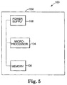
- One embodiment of a computer system according to the present invention is illustrated generally at 100 in FIG. 5 in block diagram form.
- the computer system 100 includes a housing 102 surrounds electronic components and other internal components of the computer system 100.
- the computer system 1.00 includes a microprocessor 104 for performing sequences of logical operations and a memory 106 for storing instructions and data for use by the microprocessor 104.
- the memory 106 typically includes random access memory (RAM), non-volatile memory, and a hard disk drive, but can include any known type of memory storage.
- a power supply 108 supplies regulated voltage power to devices in the computer system 100, such as the microprocessor 104 and the memory 106.
- the ASIC 10 can serve as, or as part of, one or more of the electronic components of a computer system 100, such as the microprocessor 104, the memory 106, etc. Further, the ASIC 10 can serve as, or as part of, other integrated circuit components and/or discrete logic components not otherwise specifically depicted in FIG. 5.
- the ASIC design, and in particular, the operational block design of the present invention provides a marked improvement over previous designs.
- Spare logic gates are assigned and clustered into at least two subgroups.
- the so-defined subgroups are spaced from one another within the operational block boundary. This spacing, in turn, dictates that the spare gate wiring connecting the various spare logic gates will extend to outer metal layers associated with the ASIC.
- operational block repairs are easily performed by a FIB tool that readily accesses the spare gate wiring.
- the method of manufacture of the present invention requires only that spacing and/or placement instructions for the spare logic gate subgroups be provided to the automatic placement tool. The more difficult task of programming the automatic routing tool to effectuate certain spare gate wiring runs is avoided.
Landscapes
- Engineering & Computer Science (AREA)
- Computer Hardware Design (AREA)
- Physics & Mathematics (AREA)
- Theoretical Computer Science (AREA)
- Evolutionary Computation (AREA)
- Geometry (AREA)
- General Engineering & Computer Science (AREA)
- General Physics & Mathematics (AREA)
- Design And Manufacture Of Integrated Circuits (AREA)
- Internal Circuitry In Semiconductor Integrated Circuit Devices (AREA)
- Semiconductor Integrated Circuits (AREA)
Abstract
Description
Claims (20)
- An application specific integrated circuit comprising:a substrate layer;at least one metal layer formed above the substrate layer; andan operational block formed in the substrate layer and the metal layer, the operational block definable by a two-dimensional boundary and including:a plurality of operational logic gates,a first subgroup of spare logic gates,a second subgroup of spare logic gates,wherein the first subgroup is spaced from the second subgroup on the substrate layer,operational wiring formed in the metal layer interconnecting the operational logic gates to configure the operational block to perform a desired operation,spare gate wiring formed separate from the operational wiring in the at least one metal layer, the spare gate wiring connecting at least one of the first subgroup spare logic gates to at least one of the second subgroup spare logic gates.
- The application specific integrated circuit of claim 1, wherein the boundary defines a major dimension, and further wherein a spacing between the first and second subgroups is at least one-half the major dimension.
- The application specific integrated circuit of claim 2, wherein the spacing is at least two-thirds the major dimension.
- The application specific integrated circuit of claim 2, wherein the boundary is generally rectangular and defines a minor dimension, and further wherein the first and second subgroup are substantially centered along the minor dimension.
- The application specific integrated circuit of claim 1, wherein each of the first and second subgroups includes at least 25 spare logic gates.
- The application specific integrated circuit of claim 1, wherein the spare logic gates of the first subgroup are spaced from one another by approximately 2 microns.
- The application specific integrated circuit of claim 1, further comprising a plurality of metal layers including an inner metal layers positioned between outer metal layers and the substrate, and further wherein at least a portion of the spare gate wiring extends to the outer metal layers.
- The application specific integrated circuit of claim 1, further comprising:first, second, third, fourth, fifth, and sixth metal layers sequentially formed above the substrate layer such that the first metal layer is proximal the substrate layer;wherein at least a portion of the spare gate wiring extends to the fifth metal layer.
- The application specific integrated circuit of claim 8, wherein the spare gate wiring includes a plurality of wires each connecting a respective one of the first subgroup spare logic gates to a respective one of the second subgroup spare logic gates, and further wherein at least a portion of each of the plurality of wires extends to the fifth metal layer.
- The application specific integrated circuit of claim 1, wherein at least a portion of the spare gate wiring is formed to be accessible by a focused ion beam device.
- A custom computer system comprising:an application specific integrated circuit including:a substrate layer,at least one metal layer formed above the substrate layer, andan operational block formed in the substrate layer and the metal layer, the operational block definable by a two-dimensional boundary and including:a plurality of operational logic gates,a first subgroup of spare logic gates,a second subgroup of spare logic gates,wherein the first subgroup is spaced from the second subgroup on the substrate layer,operational wiring formed in the metal layer interconnecting the operational logic gates to configure the operational block to perform a desired operation,spare gate wiring formed separate from the operational wiring in the metal layer, the spare gate wiring connecting at least one of the first subgroups spare logic gates to at least one of the second subgroup spare logic gates.
- The custom computer system of claim 11, wherein the boundary defines a major dimension, and further wherein a spacing between the first and second subgroups is at least two-thirds the major dimension.
- The custom computer system of claim 11, wherein the application specific integrated circuit chip further comprises:first, second, third, fourth, fifth, and sixth metal layers sequentially formed above the substrate layer such that the first metal layer is proximal the substrate layer;wherein at least a portion of the spare gate wiring extends to the fifth metal layer.
- A method of manufacturing an operational block portion of an application specific integrated circuit, the operational block including operational logic gates for performing a desired operation, the method comprising:assigning spare logic gates to one of a first subgroup and a second subgroup;defining an abstract, two-dimensional boundary for the operational block;providing a substrate layer;forming the operational logic gates on the substrate layer, within the boundary;forming the first and second subgroups on the substrate layer such that the subgroups are spaced from one another within the boundary;forming a metal layer over the substrate layer;routing operational wiring in the metal layer interconnecting the operational logic gates to configure the operational block to perform a desired operation; androuting spare gate wiring in the metal layer, the spare gate wiring connecting at least one of the first subgroup spare gates to at least one of the second subgroup spare gates.
- The method of claim 14, wherein the boundary is definable by a major dimension, and further wherein forming the first and second subgroup includes spacing the first subgroup from the second subgroup by a distance of at least one-half the major dimension.
- The method of claim 15, wherein the distance between the first and second subgroups is at least two-thirds the major dimension.
- The method of claim 15, wherein the subgroups are formed by a gate placement tool, the method further comprising:
providing programming instructions to the gate placement tool requiring that the first subgroup be spaced from the second subgroup by the distance of at least one-half the major dimension. - The method of claim 14, further comprising:forming a plurality of metal layers over the substrate layer, the plurality of metal layers including inner layers, outer layers above the inner layers;wherein routing the spare gate wiring includes forming at least a portion of the spare gate wiring in at least one of the outer layers.
- The method of claim 18, wherein the plurality of metal layers includes a first, second, third, fourth, fifth, and sixth metal layers sequentially formed over the substrate layer such that the first metal layer is proximal the substrate layer, and further wherein routing the spare gate wiring includes forming at least a portion of the spare gate wiring in the fifth layer.
- The method of claim 18, wherein an automatic routing tool routes the spare gate wiring, the method further comprising:
establishing a minimum spacing between the subgroups, the minimum spacing being selected to force the automatic routing tool to form a portion of the spare gate wiring in the outer layers.
Applications Claiming Priority (2)
| Application Number | Priority Date | Filing Date | Title |
|---|---|---|---|
| US561725 | 2000-05-01 | ||
| US09/561,725 US6480990B1 (en) | 2000-05-01 | 2000-05-01 | Application specific integrated circuit with spaced spare logic gate subgroups and method of fabrication |
Publications (2)
| Publication Number | Publication Date |
|---|---|
| EP1152468A2 true EP1152468A2 (en) | 2001-11-07 |
| EP1152468A3 EP1152468A3 (en) | 2007-07-18 |
Family
ID=24243165
Family Applications (1)
| Application Number | Title | Priority Date | Filing Date |
|---|---|---|---|
| EP01108614A Withdrawn EP1152468A3 (en) | 2000-05-01 | 2001-04-05 | Application specific integrated circuit with spaced spare logic gate subgroups and method of fabrication |
Country Status (3)
| Country | Link |
|---|---|
| US (1) | US6480990B1 (en) |
| EP (1) | EP1152468A3 (en) |
| JP (1) | JP2007053118A (en) |
Cited By (1)
| Publication number | Priority date | Publication date | Assignee | Title |
|---|---|---|---|---|
| EP4567885A1 (en) * | 2023-12-07 | 2025-06-11 | Intel Corporation | Method to enable logic for focused ion beam circuit edit in the uppermost routing layers |
Families Citing this family (5)
| Publication number | Priority date | Publication date | Assignee | Title |
|---|---|---|---|---|
| US6922817B2 (en) * | 2003-04-04 | 2005-07-26 | Lsi Logic Corporation | System and method for achieving timing closure in fixed placed designs after implementing logic changes |
| US20090045836A1 (en) * | 2007-08-15 | 2009-02-19 | Herzl Robert D | Asic logic library of flexible logic blocks and method to enable engineering change |
| US20090045839A1 (en) * | 2007-08-15 | 2009-02-19 | International Business Machines Corporation | Asic logic library of flexible logic blocks and method to enable engineering change |
| US7480888B1 (en) | 2008-05-21 | 2009-01-20 | International Business Machines Corporation | Design structure for facilitating engineering changes in integrated circuits |
| US20230274066A1 (en) | 2022-02-23 | 2023-08-31 | D2S, Inc. | Concurrently routing multiple partitions of an integrated circuit design |
Family Cites Families (12)
| Publication number | Priority date | Publication date | Assignee | Title |
|---|---|---|---|---|
| US5016080A (en) * | 1988-10-07 | 1991-05-14 | Exar Corporation | Programmable die size continuous array |
| JP2871821B2 (en) * | 1989-09-13 | 1999-03-17 | 日本電気株式会社 | Peripheral drive circuit |
| US5122685A (en) | 1991-03-06 | 1992-06-16 | Quicklogic Corporation | Programmable application specific integrated circuit and logic cell therefor |
| US5434514A (en) * | 1992-11-19 | 1995-07-18 | Altera Corporation | Programmable logic devices with spare circuits for replacement of defects |
| US5432464A (en) | 1993-09-29 | 1995-07-11 | Societe D'applications Generales D'electricite Et De Mecanique Sagem | Application specific integrated circuit including a microprocessor for customized functions as defined by the user |
| US5696943A (en) * | 1995-07-27 | 1997-12-09 | Advanced Micro Devices, Inc. | Method and apparatus for quick and reliable design modification on silicon |
| US5706292A (en) * | 1996-04-25 | 1998-01-06 | Micron Technology, Inc. | Layout for a semiconductor memory device having redundant elements |
| US5796662A (en) | 1996-11-26 | 1998-08-18 | International Business Machines Corporation | Integrated circuit chip with a wide I/O memory array and redundant data lines |
| US6307162B1 (en) * | 1996-12-09 | 2001-10-23 | International Business Machines Corporation | Integrated circuit wiring |
| US6022791A (en) * | 1997-10-15 | 2000-02-08 | International Business Machines Corporation | Chip crack stop |
| US5959905A (en) | 1997-10-31 | 1999-09-28 | Vlsi Technology, Inc. | Cell-based integrated circuit design repair using gate array repair cells |
| US5936876A (en) | 1997-12-03 | 1999-08-10 | Lsi Logic Corporation | Semiconductor integrated circuit core probing for failure analysis |
-
2000
- 2000-05-01 US US09/561,725 patent/US6480990B1/en not_active Expired - Fee Related
-
2001
- 2001-04-05 EP EP01108614A patent/EP1152468A3/en not_active Withdrawn
- 2001-04-26 JP JP2001128946A patent/JP2007053118A/en active Pending
Cited By (1)
| Publication number | Priority date | Publication date | Assignee | Title |
|---|---|---|---|---|
| EP4567885A1 (en) * | 2023-12-07 | 2025-06-11 | Intel Corporation | Method to enable logic for focused ion beam circuit edit in the uppermost routing layers |
Also Published As
| Publication number | Publication date |
|---|---|
| US6480990B1 (en) | 2002-11-12 |
| EP1152468A3 (en) | 2007-07-18 |
| JP2007053118A (en) | 2007-03-01 |
Similar Documents
| Publication | Publication Date | Title |
|---|---|---|
| CN100416789C (en) | Method of arranging chips on first substrate on second and third substrates | |
| KR100187872B1 (en) | A semiconductor chip kerf clear method for forming semiconductor chips and electronic module therefor | |
| US9564379B2 (en) | Via chains for defect localization | |
| EP1065721A2 (en) | Standard cells and method for placing and routing thereof | |
| KR100583164B1 (en) | Integrated circuit bus grid with wires with preselectable variable width | |
| US9728474B1 (en) | Semiconductor chips with seal rings and electronic test structures, semiconductor wafers including the semiconductor chips, and methods for fabricating the same | |
| US20200303268A1 (en) | Semiconductor device including residual test pattern | |
| US6480990B1 (en) | Application specific integrated circuit with spaced spare logic gate subgroups and method of fabrication | |
| US20250149391A1 (en) | Semiconductor device and method of forming the same | |
| US6686224B2 (en) | Chip manufacturing method for cutting test pads from integrated circuits by sectioning circuit chips from circuit substrate | |
| KR20070095322A (en) | A semiconductor chip having an identification code, a method of manufacturing the chip, and a semiconductor chip management system | |
| US5976980A (en) | Method and apparatus providing a mechanical probe structure in an integrated circuit die | |
| US6150718A (en) | Method and apparatus for performing a circuit edit through the back side of an integrated circuit die | |
| US8056025B1 (en) | Integration of open space/dummy metal at CAD for physical debug of new silicon | |
| US5345394A (en) | Method for generating power slits | |
| JP2003031677A (en) | Method for manufacturing semiconductor integrated circuit and method for designing the same, and semiconductor integrated circuit | |
| US20020162997A1 (en) | Semiconductor chip | |
| JP3965911B2 (en) | Design method of master slice type semiconductor integrated circuit | |
| US20040232414A1 (en) | Interconnect routing over semiconductor for editing through the back side of an integrated circuit | |
| US20230154860A1 (en) | Semiconductor chip including align mark protection pattern and semiconductor package including semiconductor chip including the align mark protection pattern | |
| US20050285229A1 (en) | Semiconductor device and method of manufacturing the same | |
| CN116705750A (en) | Multifunctional semiconductor device substrate, semiconductor device assembly using the same, and method of forming the same | |
| KR100621814B1 (en) | A computer implemented method for packaging a semiconductor device and a computer implemented method of packaging a semiconductor die | |
| CN113921501A (en) | Semiconductor device and method for manufacturing the same | |
| EP4607538A1 (en) | Ion trap device including a substrate with an opening for electrical coupling elements |
Legal Events
| Date | Code | Title | Description |
|---|---|---|---|
| PUAI | Public reference made under article 153(3) epc to a published international application that has entered the european phase |
Free format text: ORIGINAL CODE: 0009012 |
|
| AK | Designated contracting states |
Kind code of ref document: A2 Designated state(s): AT BE CH CY DE DK ES FI FR GB GR IE IT LI LU MC NL PT SE TR |
|
| AX | Request for extension of the european patent |
Free format text: AL;LT;LV;MK;RO;SI |
|
| PUAL | Search report despatched |
Free format text: ORIGINAL CODE: 0009013 |
|
| AK | Designated contracting states |
Kind code of ref document: A3 Designated state(s): AT BE CH CY DE DK ES FI FR GB GR IE IT LI LU MC NL PT SE TR |
|
| AX | Request for extension of the european patent |
Extension state: AL LT LV MK RO SI |
|
| RIC1 | Information provided on ipc code assigned before grant |
Ipc: G06F 11/20 20060101ALN20070611BHEP Ipc: G06F 17/50 20060101ALI20070611BHEP Ipc: H01L 27/02 20060101ALI20070611BHEP Ipc: H01L 27/118 20060101AFI20010727BHEP |
|
| 17P | Request for examination filed |
Effective date: 20071219 |
|
| AKX | Designation fees paid |
Designated state(s): DE FR GB |
|
| 17Q | First examination report despatched |
Effective date: 20080723 |
|
| STAA | Information on the status of an ep patent application or granted ep patent |
Free format text: STATUS: THE APPLICATION IS DEEMED TO BE WITHDRAWN |
|
| 18D | Application deemed to be withdrawn |
Effective date: 20091103 |