EP1152433A1 - Semiconductor storage device - Google Patents
Semiconductor storage device Download PDFInfo
- Publication number
- EP1152433A1 EP1152433A1 EP00979993A EP00979993A EP1152433A1 EP 1152433 A1 EP1152433 A1 EP 1152433A1 EP 00979993 A EP00979993 A EP 00979993A EP 00979993 A EP00979993 A EP 00979993A EP 1152433 A1 EP1152433 A1 EP 1152433A1
- Authority
- EP
- European Patent Office
- Prior art keywords
- bit line
- sub
- voltage
- complementary
- input node
- Prior art date
- Legal status (The legal status is an assumption and is not a legal conclusion. Google has not performed a legal analysis and makes no representation as to the accuracy of the status listed.)
- Withdrawn
Links
Images




Classifications
-
- G—PHYSICS
- G11—INFORMATION STORAGE
- G11C—STATIC STORES
- G11C7/00—Arrangements for writing information into, or reading information out from, a digital store
-
- G—PHYSICS
- G11—INFORMATION STORAGE
- G11C—STATIC STORES
- G11C16/00—Erasable programmable read-only memories
- G11C16/02—Erasable programmable read-only memories electrically programmable
- G11C16/06—Auxiliary circuits, e.g. for writing into memory
- G11C16/26—Sensing or reading circuits; Data output circuits
- G11C16/28—Sensing or reading circuits; Data output circuits using differential sensing or reference cells, e.g. dummy cells
-
- G—PHYSICS
- G11—INFORMATION STORAGE
- G11C—STATIC STORES
- G11C7/00—Arrangements for writing information into, or reading information out from, a digital store
- G11C7/06—Sense amplifiers; Associated circuits, e.g. timing or triggering circuits
- G11C7/065—Differential amplifiers of latching type
-
- G—PHYSICS
- G11—INFORMATION STORAGE
- G11C—STATIC STORES
- G11C7/00—Arrangements for writing information into, or reading information out from, a digital store
- G11C7/12—Bit line control circuits, e.g. drivers, boosters, pull-up circuits, pull-down circuits, precharging circuits, equalising circuits, for bit lines
-
- G—PHYSICS
- G11—INFORMATION STORAGE
- G11C—STATIC STORES
- G11C7/00—Arrangements for writing information into, or reading information out from, a digital store
- G11C7/18—Bit line organisation; Bit line lay-out
Definitions
- the present invention relates to a semiconductor memory device, and in particular to a semiconductor memory device which allows information to be read from a memory cell with a high speed.
- the required memory capacity is also on the increase with recent enhancements in the functions of microcomputers.
- the present invention aims to provide a semiconductor memory device which is capable of reading information from memory cells with a high speed.
- a semiconductor memory device comprises: a differential sense amplifier having a first input node and a second input node for sensing a difference between a voltage on the first input node and a voltage on the second input node; an information read section for supplying a voltage varying in accordance with information which is read from a memory cell, the voltage being supplied to the first input node; a reference section for supplying a reference voltage to the second input node; and a control section for controlling the differential sense amplifier, the information read section, and the reference section, wherein the information read section includes: a main bit line coupled to the first input node; a select gate; a sub-bit line which is coupled to the main bit line via the select gate; a memory cell which is coupled to the sub-bit line and which is selectively activated in accordance with a voltage on a word line; a precharge section for precharging the first input node and the main bit line to a first voltage; and a reset section for resetting the sub-bit line to a second
- the information read section may further comprise: a first capacitance coupled to the main bit line; and a second capacitance coupled to the sub-bit line.
- a voltage on the sub-bit line after the charge which is precharged in the first input node and the main bit line is redistributed may be equal to or less than about 1 V.
- the reference section may comprise: a complementary main bit line coupled to the second input node; and a precharge section for precharging the second input node and the complementary main bit line to a third voltage, wherein the third voltage is equal to a voltage which is obtained by multiplying the first voltage by a predetermined ratio.
- the reference section may output the reference voltage by using a reference cell haying a current performance which is substantially half of a current performance of the memory cell.
- the differential sense amplifier may sense the difference between the voltage on the first input node and the voltage on the second input node through sense integration.
- the sense integration may be begun while a portion of a charge which is precharged in the first input node and the main bit line is redistributed to the sub-bit line.
- Another semiconductor memory device comprises: a differential sense amplifier having a first input node and a second input node for sensing a difference between a voltage on the first input node and a voltage on the second input node; a main bit line coupled to the first input node; a complementary main bit line coupled to the second input node; a precharge section for precharging the main bit line and the complementary main bit line to a first voltage; a plurality of subarrays arranged in a direction along which the main bit line and the complementary main bit line extend; and a control section for controlling the differential sense amplifier, the precharge section, and the plurality of subarrays, wherein each of the plurality of subarrays includes: a select gate section for selectively coupling the main bit line to one of a plurality of sub-bit lines and selectively coupling the complementary main bit line to one of a plurality of complementary sub-bit lines; a reset section for resetting the plurality of sub-bit lines to a second voltage which is lower than the
- the control section may control the plurality of subarrays so as to maintain a reset state of at least one sub-bit line adjoining the sub-bit line to which the charge has been redistributed from the main bit line, and to maintain a reset state of at least one complementary sub-bit line adjoining the complementary sub-bit line to which the charge has been redistributed from the complementary main bit line.
- Another semiconductor memory device comprises: a differential sense amplifier having a first input node and a second input node for sensing a difference between a voltage on the first input node and a voltage on the second input node; a main bit line coupled to the first input node; a complementary main bit line coupled to the second input node; a precharge section for precharging the main bit line and the complementary main bit line to a first voltage; a plurality of subarrays arranged in a direction along which the main bit line and the complementary main bit line extend; and a control section for controlling the differential sense amplifier, the precharge section, and the plurality of subarrays, wherein each of the plurality of subarrays includes: a select gate section for selectively coupling the main bit line to one of a plurality of sub-bit lines and selectively coupling the complementary main bit line to one of a plurality of complementary sub-bit lines; a reset section for resetting the plurality of sub-bit lines to a second voltage which is lower than the
- the control section may control the plurality of subarrays so as to maintain a reset state of at least one sub-bit line adjoining the sub-bit line to which the charge has been redistributed from the main bit line, and to maintain a reset state of at least one complementary sub-bit line adjoining the complementary sub-bit line to which the charge has been redistributed from the complementary main bit line.
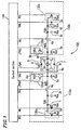
- Figure 1 is a diagram illustrating the structure of a semiconductor memory device 100 according to Example 1 of the present invention.
- Figure 2 is a timing chart illustrating an operation of the semiconductor memory device 100.
- Figure 3 is a diagram schematically illustrating an operation of the semiconductor memory device 100 .
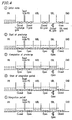
- Figure 4 is a diagram schematically illustrating an operation of a conventional semiconductor memory device.
- Figure 5 is a diagram illustrating the structure of a semiconductor memory device 200 according to Example 2 of the present invention.
- Figure 6 is a timing chart illustrating an operation of the semiconductor memory device 200 .
- Figure 1 illustrates the structure of a semiconductor memory device 100 according to Example 1 of the present invention.
- the semiconductor memory device 100 may be, for example, a non-volatile semiconductor memory device.
- the semiconductor memory device 100 includes a differential sense amplifier 9 having a first input node in the form of an input node 9a and a second input node in the form of an input node 9b .
- the differential sense amplifier 9 determines the value of information which is read from a memory cell 1 by sensing a difference between the voltage on the input node 9a and the voltage on the input node 9b . For example, the differential sense amplifier 9 determines that the value of the information which is read from the memory cell 1 is "1" if the difference between the voltage on the input node 9a and the voltage on the input node 9b is greater than a predetermined threshold voltage, and otherwise determines that the value of the information which is read from the memory cell 1 is "0".
- the semiconductor memory device 100 includes: an information read section 110a for supplying a voltage which varies in accordance with the information which is read from the memory cell 1 to the input node 9a; a reference section 110b for supplying a reference voltage to the input node 9b; and a control section 140 for controlling the differential sense amplifier 9, the information read section 110a, and the reference section 110b.
- the information read section 110a includes: a main bit line MBL which is coupled to the input node 9a; a sub-bit line SBL which is coupled to the main bit line MBL via a select gate 4a; a memory cell 1 which is coupled to the sub-bit line SBL and which is selectively activated in accordance with a voltage on a word line WL; a precharge section 120a for precharging the input node 9a and the main bit line MBL to a supply voltage V dd which defines a first voltage; and a reset section 130a for resetting the sub-bit line SBL to a ground voltage V ss which defines a second voltage.
- the select gate 4a is turned on when a select gate signal SG is at a high level, and turned off when the select gate signal SG is at a low level.
- the select gate signal SG is supplied from the control section 140 to the select gate 4a.
- the precharge section 120a includes a Pch transistor 6a.
- One terminal of the Pch transistor 6a is coupled to a supply voltage V dd .
- Another terminal of the Pch transistor 6a is coupled to the main bit line MBL.
- the Pch transistor 6a is turned off when a precharge signal /PRC is at a high level, and turned on when the precharge signal /PRC is at a low level.
- the input node 9a and the main bit line MBL are precharged to the supply voltage V dd when the precharge signal /PRC is at the low level.
- the precharge signal /PRC is supplied from the control section 140 to the precharge section 120a.
- the reset section 130a includes an Nch transistor 2a.
- One terminal of the Nch transistor 2a is coupled to a sub-bit line SBL, and another terminal of the Nch transistor 2a is coupled to the ground voltage V ss .
- the Nch transistor 2a is turned on when a reset signal RS is at a high level, and turned off when the reset signal RS is at a low level.
- the sub-bit line SBL is reset to the ground voltage V ss when the reset signal RS is at the high level.
- the reset signal RS is supplied from the control section 140 to the reset section 130a.
- a capacitance 5a is coupled to the main bit line MBL.
- the capacitance 5a includes the stray capacitance of the main bit line MBL itself.
- a capacitance 3a is coupled to the sub-bit line SBL.
- the capacitance 3a includes the stray capacitance of the sub-bit line SBL itself.
- the reference section 110b includes: a complementary main bit line /MBL which is coupled to the input node 9b; a complementary sub-bit line /SBL which is coupled to the complementary main bit line /MBL via a select gate 4b; a reference cell 10 which is coupled to the complementary sub-bit line /SBL and which is selectively activated in accordance with a voltage on the reference word line DWL; a precharge section 120b for precharging the input node 9b and the complementary main bit line /MBL to the supply voltage V dd which defines the first voltage; and a reset section 130b for resetting the complementary sub-bit line /SBL to the ground voltage V ss which defines the second voltage.
- the ground voltage V ss is lower than the supply voltage V dd .
- the structure of the select gate 4b, the precharge section 120b, and the reset section 130b is the same as the structure of the select gate 4a, the precharge section 120a, and the reset section 130a.
- the current performance of the reference cell 10 is adjusted so as to be substantially half of the current performance of the memory cell 1.
- the reference cell 10 may be a memory cell which includes a floating gate containing no electrons and whose channel width is substantially 1/2 that of the memory cell 1.
- the precharge section 120b may be arranged so as to precharge the input node 9b and the complementary main bit line /MBL to a voltage obtained by multiplying the supply voltage V dd by a predetermined ratio ⁇ (where 0 ⁇ ⁇ ⁇ 1).
- the precharge section 120b can also supply a reference voltage to the input node 9b.
- a capacitance 5b is coupled to the complementary main bit line /MBL.
- the capacitance 5b includes the stray capacitance of the complementary main bit line /MBL itself.
- a capacitance 3b is coupled to the complementary sub-bit line /SBL.
- the capacitance 3b includes the stray capacitance of the complementary sub-bit line /SBL itself.
- Figure 2 illustrates an operation of the semiconductor memory device 100.
- the reset signal RS is at a high level; the precharge signal /PRC is at a low level; the select gate signal SG is at a low level; and the word line WL and the reference word line DWL are at a low level.
- the input node 9a and the main bit line MBL are precharged to the supply voltage V dd , and the sub-bit line SBL is reset to the ground voltage V ss .
- the input node 9b and the complementary main bit line /MBL are precharged to the supply voltage V dd , and the complementary sub-bit line /SBL is reset to the ground voltage V ss .
- the reset signal RS shifts from the high level to a low level
- the precharge signal /PRC shifts from the low level to a high level.
- the select gate signal SG, the word line WL, and the reference word line DWL are activated.
- the select gate signal SG, the word line WL , and the reference word line DWL shown in Figure 1 are selected in accordance with the address signal.
- the select gate signal SG, the word line WL , and the reference word line DWL all shift from the respective low levels to the respective high levels.
- V SBL ⁇ C m / (C s + C m ) ⁇ ⁇ V dd
- C m represents the capacitance value of the capacitance 5a
- C s represents the capacitance value of the capacitance 3a.
- the voltage V SBL is equal to the voltage obtained by subjecting the supply voltage V dd to a capacitive division in accordance with capacitance values C m and C s .
- the time required for the voltage on the sub-bit line SBL to be stabilized to the voltage V SBL is determined based on a time constant which is based on a series capacitance of the capacitances 5a and 3a as well as the impedance of the select gate 4a.
- the voltage V SBL on the sub-bit line SBL after the charge redistribution is equal to or less than about 1 V because a read disturbance must be avoided in the case of a common NOR-type flash memory or the like, although this is not true where there is no read disturbance.
- the voltage V SBL is about 1 V
- the high level of the select gate 4a is equal to or greater than about 2.5 V
- the threshold voltage of the select gate 4a is about 0.5 V
- the value of the voltage V SBL can be easily adjusted by adjusting the ratio between the capacitance values C m and C s .
- the value of the voltage V SBL may be adjusted by varying the level of the supply voltage V dd .
- the transition of the voltage on the main bit line MBL in the case where the value of the information stored in the memory cell 1 is "1" is illustrated as MBL "1".
- the transition of the voltage on the sub-bit line SBL in the case where the value of the information stored in the memory cell 1 is "1" is illustrated as SBL "1".
- the transition of the voltage on the main bit line MBL in the case where the value of the information stored in the memory cell 1 is "0" is illustrated as MBL "0".
- the transition of the voltage on the sub-bit line SBL in the case where the value of the information stored in the memory cell 1 is "0" is illustrated as SBL "0".
- the transition of the voltage on the complementary main bit line /MBL is intermediate between the transition of the voltage on the main bit line MBL in the case where the value of the information stored in the memory cell 1 is "1" and the transition of the voltage on the main bit line MBL in the case where the value of the information stored in the memory cell 1 is "0". This is because, as described above, the current performance of the reference cell 10 is previously adjusted so as to be substantially half of the current performance of the memory cell 1.
- the differential sense amplifier 9 is activated in response to an enable signal SAE.
- the differential sense amplifier 9 outputs information which indicates whether the value of the information which has been read from the memory cell 1 is "1" or "0" when the difference between the voltage on the main bit line MBL and the voltage on the complementary main bit line /MBL becomes sufficiently large.
- the differential sense amplifier 9 is a CMOS latch type differential sense amplifier.
- a CMOS latch type differential sense amplifier can be suitably used as the differential sense amplifier 9 because it is capable of operating in a broad voltage range with a high speed, requires a small layout area, and has a high driving performance.
- the differential sense amplifier 9 is not limited to this type of differential sense amplifier, but may be any type of differential sense amplifier.
- the differential sense amplifier 9 may be a differential sense amplifier of a current driving type.
- Figure 3 schematically illustrates the operation of the semiconductor memory device 100 .
- the operation of the information read section 110a will be described assuming that the value of the information stored in the memory cell 1 is "0".
- the operation of the reference section 110b is similar to the operation of the information read section 110a.
- each tub represents an element in the information read section 110a.
- the size of each tub represents the capacitance value of each element.
- the water level in each tub represents the voltage of that element.
- PR represents a precharge source for supplying the supply voltage V dd
- GND represents a ground source for supplying the ground voltage V ss .
- the capacitance value C m in eq. 1 corresponds to a sum of the capacitance value of the input node 9a and the capacitance value of the main bit line MBL.
- the input node 9a and the main bit line MBL are coupled to the precharge source PR via a precharge gate.
- the precharge gate corresponds to the Pch transistor 6a shown in Figure 1.
- the sub-bit line SBL is coupled to the main bit line MBL via an SG gate.
- the SG gate corresponds to the select gate 4a shown in Figure 1.
- the sub-bit line SBL is coupled to the ground source GND via an SBL reset gate.
- the SBL reset gate corresponds to the Nch transistor 2a shown in Figure 1.
- a WL gate is coupled to the sub-bit line SBL.
- the WL gate corresponds to the memory cell 1 shown in Figure 1. In other words, the WL gate is "open” when the value of the information stored in the memory cell 1 is "0" and the memory cell 1 is activated; otherwise, the WL gate is "closed”.
- the precharge gate and the SBL reset gate become "open", whereas the SG gate and the WL gate become “closed”.
- the input node 9a and the main bit line MBL are precharged by the precharge source PR
- the sub-bit line SBL is reset by the ground source GND.
- the precharge gate and the SBL reset gate become "closed", and the SG gate and the WL gate, as selected in accordance with an input address signal, become “open” .
- a portion of the charge which is precharged in the input node 9a and the main bit line MBL migrates, via the SG gate, to the sub-bit line SBL (charge redistribution).
- the sub-bit line SBL is charged as a result of the charge redistribution.
- a current flows out from the WL gate.
- a sense integration can be begun before the charging of the sub-bit line SBL is completed. Since the current flowing out from the WL gate is sufficiently small as compared with the current flowing from the main bit line MBL to the sub-bit line SBL, the voltage on the sub-bit line SBL quickly increases.
- the integration period continues.
- the voltage on the main bit line MBL gradually decreases while charge redistribution occurs and as a current flows out from the WL gate.
- the differential sense amplifier 9 outputs information indicating the value of the information which has been read from the memory cell 1 .
- the sub-bit line SBL is precharged by utilizing charge redistribution.
- a current flows from the memory cell 1 to the ground voltage V ss .
- the sub-bit line SBL is discharged.
- Such a discharging of the sub-bit line SBL occurs concurrently with the precharging of the sub-bit line SBL, without waiting for the charge redistribution to finish.
- the time required for the precharging of the sub-bit line SBL and the integration of the charge which has been released from the memory cell 1 can be reduced.
- the time required for the charge redistribution can be reduced to an almost negligible level because it is easy to design the time constant based on the impedance of the select gate 4a and the capacitances 5a and 3a so as to be sufficiently small. For example, by securing a sufficiently high current driving performance in the transistor used for the select gate 4a, it is possible to design the time constant so as to be sufficiently small. This substantially contributes to the enhancement of the read rate of information from the memory cell 1 .
- the precharging of the main bit line MBL can occur before ascertaining an address.
- the reading of information from the memory cell 1 can be made faster.
- the precharging of the main bit line MBL may be performed during a period from the completion of the sense operation by the differential sense amplifier 9 until the receipt of a next address. As a result, it is possible to assume that there is apparently no precharge period for precharging the main bit line MBL.
- a semiconductor memory device 100 can be provided which is capable of reading information from the memory cell 1 with a high speed.
- Figure 4 schematically illustrates the operation of a conventional semiconductor memory device described in the aforementioned publication, for comparison with Figure 3 . In the following description, it is assumed that the value of the information stored in the memory cell is "0".
- each tub represents an element required for reading information from the memory cell.
- the size of each tub represents the capacitance value of each element.
- the water level in each tub represents the voltage of that element.
- the capacitance values of the precharge source PR and the ground source GND are infinite, and that the capacitance values of one input node (hereinafter referred to as an input node P0 ) of the differential sense amplifier, the main bit line MBL, and the sub-bit line SBL are finite.
- the input node P0 is coupled to the precharge source PR via a precharge gate.
- the main bit line MBL is coupled to the input node P0 via a Y gate.
- the sub-bit line SBL is coupled to the main bit line MBL via an SG gate.
- the sub-bit line SBL is coupled to the ground source GND via an SBL reset gate.
- a WL gate is coupled to the sub-bit line SBL .
- the WL gate is "open” when the value of the information stored in the memory cell is "0" and the memory cell is activated; otherwise, the WL gate is "closed”.
- the SBL reset gate becomes "open", whereas the other gates become “closed”.
- the input node P0, the main bit line MBL, and the sub-bit line SBL are reset by the ground source GND.
- the main bit line MBL also has an MBL reset gate, it is not shown.
- the precharge gate becomes "open", and the SBL reset gate becomes “closed”. Moreover, the Y gate, the SG gate, and the WL gate, as selected in accordance with an input address signal, become "open". Herein, it is assumed that the Y gate, the SG gate, and the WL gate shown in Figure 4 are selected. As a result, the input node P0, the main bit line MBL, and the sub-bit line SBL are precharged by the precharge source PR. The time constant at this time is determined based on the series capacitance of the series impedance of the precharge gate, the Y gate, and the SG gate, and the parallel capacitance of the main bit line MBL and the sub-bit line SBL.
- the precharge is completed when the voltages on the input node P0, the main bit line MBL, and the sub-bit line SBL have increased to the voltage on the precharge source PR.
- the precharge gate becomes "closed” .
- the precharge source PR is electrically isolated from the input node P0, the main bit line MBL, and the sub-bit line SBL.
- a sense integration can be started after the precharge gate has become “closed”.
- an integration period starts at the time when the precharge gate has become "closed”.
- the integration period continues.
- the voltages on the input node P0, the main bit line MBL, and the sub-bit line SBL gradually decrease as a current flows out from the WL gate.
- the differential sense amplifier outputs information indicating the value of the information which has been read from the memory cell.
- a precharge operation is started after the ascertainment of an address, and an integration operation is started after the completion of the precharge operation. Therefore, the time required for reading information from the memory cell is equal to a sum of a precharge time (tPRC) and an integration time (tInteg) (i.e., tPRC + tInteg).
- tPRC precharge time
- tInteg integration time
- a sense integration occurs concurrently with the charging of the sub-bit line SBL . Therefore, the time required for reading information from the memory cell 1 is equal to t (PRC + Integ) (see Figure 2 ).
- t(PRC + Integ) ⁇ tPRC + tInteg.
- Example 1 illustrates an example in which the present invention is applied to a semiconductor memory device based on an open bit line method
- the applications of the present invention are not limited thereto.
- the present invention can be applied to a semiconductor memory device based on a folded bit line method.
- Figure 5 illustrates the structure of a semiconductor memory device 200 according to Example 2 of the present invention.
- the semiconductor memory device 200 may be, for example, a non-volatile semiconductor memory device.
- the semiconductor memory device 200 includes a differential sense amplifier 9 having a first input node 9a (P0) and a second input node 9b (N0).
- a main bit line MBL is coupled to the input node 9a via a main bit line isolation gate 11a.
- a complementary main bit line /MBL is coupled to the input node 9b via a main bit line isolation gate 11b.
- the semiconductor memory device 200 further includes a precharge section 6'G for precharging the input nodes 9a and 9b to a supply voltage V dd , and a precharge section 6G for precharging the main bit line MBL and the complementary main bit line /MBL to the supply voltage V dd .
- the precharge section 6'G includes Pch transistors 6'a and 6'b which are turned on or off in accordance with a precharge signal /PRC.
- the precharge section 6G includes Pch transistors 6a and 6b which are turned on or off in accordance with the precharge signal /PRC, and an equalizing transistor 12.
- the semiconductor memory device 200 further includes a plurality of subarrays 210 to 240 which are arranged in a direction along which the main bit line MBL and the complementary main bit line /MBL extend.
- Each of the plurality of subarrays 210 to 240 is constructed so as to include the information read section 110a and the reference section 110b as shown in Figure 1 , the information read section 110a and the reference section 110b being used in common.
- the semiconductor memory device 200 further includes a control section 340 for controlling the differential sense amplifier 9, the precharge sections 6'G and 6G and the plurality of subarrays 210 to 240.
- the control section 340 outputs signals shown in Figure 5, e.g., the precharge signal /PRC, reset signals RS 00 and RS 01 , and select gate signals SGY 00 to SGY 03 and SGY 10 to SGY 13 .
- the subarray 210 includes: a memory cell array 1G including a plurality of memory cells 1; a reference cell array 10G including a plurality of reference cells 10; a select gate section 4G for selectively coupling the main bit line MBL to one of a plurality of sub-bit lines SBL 1 to SBL 2 and for selectively coupling the complementary main bit line /MBL to one of a plurality of complementary sub-bit lines / SBL 1 to /SBL 2 ; and a reset gate section 2G for previously resetting the sub-bit lines SBL 1 to SBL 2 and the complementary sub-bit lines /SBL 1 to /SBL 2 to the voltage V ss and for selectively releasing the resetting of one of the sub-bit lines SBL 1 to SBL 2 and one of the complementary sub-bit lines /SBL 1 to /SBL 2 .
- the subarray 220 has a similar structure to that of the subarray 210. However, each of the plurality of memory cells 1 included in the subarray 210 is selectively activated by a voltage on a corresponding word line among word lines WL 1 to WL n , whereas each of the plurality of memory cells 1 included in the subarray 220 is selectively activated by a voltage on a corresponding word line among word lines WL' 1 to WL' n .
- Each of the plurality of reference cells 10 included in the subarray 210 is selectively activated by a voltage on a reference word line DWL', whereas each of the plurality of reference cells 10 included in the subarray 220 is selectively activated by a voltage on a reference word line DWL .
- one of the plurality of memory cells 1 in the subarray 210 is selected, one of the plurality of reference cells 10 in the subarray 220 is selected.
- one of the plurality of memory cells 1 in the subarray 220 is selected, one of the plurality of reference cells 10 in the subarray 210 is selected.
- the subarray 210 and the subarray 220 operate in a complementary manner to each other.
- the input node 9a of the differential sense amplifier is coupled to the main bit line MBL
- the input node 9b of the differential sense amplifier is coupled to the complementary main bit line /MBL in the semiconductor memory device 200 shown in Figure 5
- the line coupled to the input node 9a of the differential sense amplifier may become the complementary main bit line /MBL
- the line coupled to the input node 9b of the differential sense amplifier may become the main bit line MBL.
- the structure of the subarrays 230 and 240 is similar to that of the subarrays 210 and 220. However, a summarized illustration of the structure of the subarrays 230 and 240 is presented for conciseness. The subarrays 230 and 240 also operate in a complementary manner to each other, like the subarrays 210 and 220.
- At least one of the plurality of memory cells 1 included in the memory cell array 1G and at least one of the plurality of reference cells 10 included in the reference cell array 10G are coupled.
- To each of the complementary sub-bit lines /SBL 1 and /SBL 2 at least one of the plurality of memory cells 1 included in the memory cell array 1G and at least one of the plurality of reference cells 10 included in the reference cell array 10G are coupled.
- the control section 340 controls the precharge section 6G and the plurality of subarrays 210 to 240 so that a portion of the charge which is precharged in the main bit line MBL is redistributed to the sub-bit line which has been selectively released from resetting, and that a portion of the charge which is precharged in the complementary main bit line /MBL is redistributed to the complementary sub-bit line which has been selectively released from resetting after precharging the main bit line MBL and the complementary main bit line /MBL to the supply voltage V dd and previously resetting the sub-bit lines SBL 1 to SBL 2 and the complementary sub-bit lines /SBL 1 to /SBL 2 to the voltage V ss , and selectively releasing the resetting of one of the sub-bit lines SBL 1 to SBL 2 and one of the complementary sub-bit lines /SBL 1 to /SBL 2 .
- the semiconductor memory device 200 may include any number of subarrays . Although the number of sub-bit lines and the complementary sub-bit lines included in one subarray in the example illustrated in Figure 5 is two, this number is not limited to two. The semiconductor memory device 200 may include any number of sub-bit lines and complementary sub-bit lines.
- the main bit line MBL, the sub-bit lines SBL 1 to SBL 2 , the complementary main bit line /MBL, and the complementary sub-bit lines /SBL 1 to /SBL 2 will each have a stray capacitance.
- the main bit line MBL and the complementary main bit line /MBL in a symmetrical layout, it is possible to substantially equalize the capacitance value C m of the main bit line MBL with the capacitance value C m ' of the complementary main bit line /MBL in spite of mask misalignment or process variations (e.g., variations in the thickness of interlayer films).
- the capacitance value C m is to be designed as a value including the capacitance value from the sense amplifier isolation transistor 11a to the input node 9a.
- Figure 6 illustrates an operation of the semiconductor memory device 200.
- the input nodes 9a and 9b, the main bit line MBL, and the complementary main bit line /MBL are precharged to the supply voltage V dd .
- the sub-bit line SBL 1 to SBL 2 and the complementary sub-bit line /SBL 1 to /SBL 2 are reset to the ground voltage V ss .
- the precharge signal /PRC is inactivated. As a result, the precharging of the input nodes 9a and 9b, the main bit line MBL, and the complementary main bit line /MBL is completed.
- two of the subarrays 210 to 240 are selected that are of a complementary relationship with each other.
- the subarrays 210 and 220 have been selected.
- the select gate signal SGY 00 , the word line WL 1 , and the reference word line DWL have been selected in response to the address signal ADD, and that the SBL reset signal RS 00 has shifted from a high level to a low level.
- the SBL reset signal RS 01 remains at a high level.
- the memory cell 1 and the reference cell 10 which are circled by broke lines in Figure 5 are selected.
- the transition of the voltage on the main bit line MBL in the case where the value of the information stored in the memory cell 1 is "0" is illustrated as MBL "0.
- the transition of the voltage on the sub-bit line SBL 1 in the case where the value of the information stored in the memory cell 1 is "0" is illustrated as SBL "0.
- the transition of the voltage on the main bit line MBL in the case where the value of the information stored in the memory cell 1 is "1" is illustrated as MBL "1".
- the transition of the voltage on the sub-bit line SBL 1 in the case where the value of the information stored in the memory cell 1 is "1" is illustrated as SBL "1".
- the transition of the voltage on the complementary main bit line /MBL is illustrated as /MBL.
- the transition of the voltage on the complementary sub-bit line /SBL 1 is illustrated as /SBL.
- Example 2 since the SBL reset signal shifts from a high level to a low level, even when the reset state of the selected sub-bit line (e.g., the sub-bit line SBL 1 ) is released, the reset state of the sub-bit line (e.g., the sub-bit line SBL 2 ) adjoining that sub-bit line will not be released. Thus, by maintaining the reset state of the sub-bit line adjoining a sub-bit line to which charge from the main bit line has been redistributed, influence from the storage content in a memory cell 1 coupled to the adjoining sub-bit line can be avoided.
- the reset state of the selected sub-bit line e.g., the sub-bit line SBL 1
- the reset state of the sub-bit line e.g., the sub-bit line SBL 2
- the number of sub-bit lines which adjoin a selected sub-bit line and which are not released from resetting even when the reset state of the selected sub-bit line is released is not limited to one.
- the number of sub-bit lines which adjoin such a selected sub-bit line and which are not released from resetting may be any integer equal to or greater than two.
- the number of complementary sub-bit lines which adjoin a selected complementary sub-bit line and which are not released from resetting even when the reset state of the selected complementary sub-bit line is released is not limited to one.
- the number of complementary sub-bit lines which adjoin such a selected complementary sub-bit line and which are not released from resetting may be any integer equal to or greater than two.
- the memory cell 1 may be any type of memory cell.
- the memory cell 1 may be a NOR type 1TR flash cell, or a Split type flash cell.
- the present invention is also applicable to another type of non-volatile memory such as a mask ROM. As a result, a non-volatile memory which is capable of reading information from a memory cell with a high speed can be obtained.
- the reference cells are provided so as to be associated with the sub-bit lines (or the complementary sub-bit lines).
- the present invention is not limited to such an arrangement.
- the reference cells may be provided so as to be associated with the main bit line (or the complementary main bit line). It will be appreciated that similar effects to those described above can be obtained with such an arrangement as well.
- main bit line or sub-bit line to which a memory cell is coupled may be coupled to a reference cell which is able to flow a current which is about 1/2 the current flowing in that memory cell. It will be appreciated that similar effects to those described above can be obtained with such an arrangement as well.
- a portion of the charge which is precharged in a first input node and a main bit line is redistributed to a sub-bit line after precharging the first input node and the main bit line to a first voltage and resetting the sub-bit line to a second voltage.
Landscapes
- Read Only Memory (AREA)
- Dram (AREA)
Abstract
A semiconductor memory device 100 includes: a
differential sense amplifier 9 having an input node 9a
and an input node 9b, an information read section 110a,
a reference section 110b, and a control section 140. The
information read section 110a includes: a main bit
line MBL coupled to the input node 9a; a select gate 4a;
a sub-bit line SBL which is coupled to the main bit
line MBL via the select gate 4a; a memory cell 1 which
is coupled to the sub-bit line SBL and which is
selectively activated in accordance with a voltage on a
word line WL; a precharge section 120a for precharging
the input node 9a and the main bit line MBL to a supply
voltage Vdd; and a reset section 130b for resetting the
sub-bit line SBL to a ground voltage Vss. The control
section 140 controls the precharge section 120a, the
reset section 130a, and the select gate 4a so that a
portion of a charge which is precharged in the input
node 9a and the main bit line MBL is redistributed to the
sub-bit line SBL after precharging the input node 9a and
the main bit line MBL to the supply voltage Vdd and
resetting the sub-bit line SBL to the ground voltage Vss.
Description
The present invention relates to a semiconductor
memory device, and in particular to a semiconductor memory
device which allows information to be read from a memory
cell with a high speed.
In recent years, there has been a desire for fast
microcomputers having an operation speed of over 100 MHz.
As microcomputers become faster in operation, the
operation of ROMs and flash memories which are mounted
on the same chip as the microcomputers are also required
to become faster. Such ROMs and flash memories are
usually mounted on a chip for the purpose of customizing
the chip.
The required memory capacity is also on the
increase with recent enhancements in the functions of
microcomputers.
Against such a background, vigorous research and
development activities are being made to realize large
capacity semiconductor memory devices which are capable
of fast read operations. For example, a semiconductor
memory device based on a hierarchical bit line method has
been proposed.
M. Hiraki et al. (ISSCC Digest of Technical Papers,
pp. 116-117, 453, Feb 1999) discloses a semiconductor
memory device based on a hierarchical bit line method.
However, in accordance with the aforementioned
type of semiconductor memory device, it is necessary to
perform an integration operation for sensing a difference
between the voltage on the main bit line and the voltage
on a complementary main bit line after completing
precharging of the main bit line and a sub-bit line.
Therefore, in order to read information from a memory cell,
a period of time (tPRC + tInteg) is required, which is
a sum of the time required for precharging the main bit
line and the sub-bit line (i.e., tPRC) and the time
required for sensing the voltage difference (i.e.,
tInteg). This has presented difficulties in the
realization of a fast read operation of information from
memory cells.
Thus, in view of the aforementioned problems, the
present invention aims to provide a semiconductor memory
device which is capable of reading information from memory
cells with a high speed.
A semiconductor memory device according to the
present invention comprises: a differential sense
amplifier having a first input node and a second input
node for sensing a difference between a voltage on the
first input node and a voltage on the second input node;
an information read section for supplying a voltage
varying in accordance with information which is read from
a memory cell, the voltage being supplied to the first
input node; a reference section for supplying a reference
voltage to the second input node; and a control section
for controlling the differential sense amplifier, the
information read section, and the reference section,
wherein the information read section includes: a main bit
line coupled to the first input node; a select gate; a
sub-bit line which is coupled to the main bit line via
the select gate; a memory cell which is coupled to the
sub-bit line and which is selectively activated in
accordance with a voltage on a word line; a precharge
section for precharging the first input node and the main
bit line to a first voltage; and a reset section for
resetting the sub-bit line to a second voltage which is
lower than the first voltage, wherein the control section
controls the precharge section, the reset section, and
the select gate so that a portion of a charge which is
precharged in the first input node and the main bit line
is redistributed to the sub-bit line after precharging
the first input node and the main bit line to the first
voltage and resetting the sub-bit line to the second
voltage. As a result, the aforementioned objective is
accomplished.
The information read section may further
comprise: a first capacitance coupled to the main bit
line; and a second capacitance coupled to the sub-bit
line.
A voltage on the sub-bit line after the charge
which is precharged in the first input node and the main
bit line is redistributed may be equal to or less than
about 1 V.
The reference section may comprise: a
complementary main bit line coupled to the second input
node; and a precharge section for precharging the second
input node and the complementary main bit line to a third
voltage, wherein the third voltage is equal to a voltage
which is obtained by multiplying the first voltage by a
predetermined ratio.
The reference section may output the reference
voltage by using a reference cell haying a current
performance which is substantially half of a current
performance of the memory cell.
The differential sense amplifier may sense the
difference between the voltage on the first input node
and the voltage on the second input node through sense
integration.
The sense integration may be begun while a portion
of a charge which is precharged in the first input node
and the main bit line is redistributed to the sub-bit line.
Another semiconductor memory device according to
the present invention comprises: a differential sense
amplifier having a first input node and a second input
node for sensing a difference between a voltage on the
first input node and a voltage on the second input node;
a main bit line coupled to the first input node; a
complementary main bit line coupled to the second input
node; a precharge section for precharging the main bit
line and the complementary main bit line to a first
voltage; a plurality of subarrays arranged in a direction
along which the main bit line and the complementary main
bit line extend; and a control section for controlling
the differential sense amplifier, the precharge section,
and the plurality of subarrays, wherein each of the
plurality of subarrays includes: a select gate section
for selectively coupling the main bit line to one of a
plurality of sub-bit lines and selectively coupling the
complementary main bit line to one of a plurality of
complementary sub-bit lines; a reset section for
resetting the plurality of sub-bit lines to a second
voltage which is lower than the first voltage, selectively
releasing the resetting of one of the plurality of sub-bit
lines, resetting the plurality of complementary sub-bit
lines to the second voltage, and selectively releasing
the resetting of one of the plurality of complementary
sub-bit lines; a memory cell array including a plurality
of memory cells; and a reference cell array including a
plurality of reference cells, wherein: each of the
plurality of memory cells is selectively activated in
accordance with a voltage on a corresponding one of a
plurality of word lines, and each of the plurality of
reference cells is selectively activated in accordance
with a voltage on a reference word line; at least one of
the plurality of memory cells and at least one of the
plurality of reference cells are coupled to each of the
plurality of sub-bit lines; at least one of the plurality
of memory cells and at least one of the plurality of
reference cells are coupled to each of the plurality of
complementary sub-bit lines; and the control section
controls the precharge section and the plurality of
subarrays so that a portion of a charge which is precharged
in the main bit line is redistributed to the sub-bit line
which has been released from resetting, and that a portion
of a charge which is precharged in the complementary main
bit line is redistributed to the complementary sub-bit
line which has been released from resetting after
precharging the main bit line and the complementary main
bit line to the first voltage and previously resetting
the plurality of sub-bit lines and the plurality of
complementary sub-bit lines to the second voltage, and
selectively releasing the resetting of one of the
plurality of sub-bit lines and one of the plurality of
complementary sub-bit lines. As a result, the
aforementioned objective is accomplished.
The control section may control the plurality of
subarrays so as to maintain a reset state of at least one
sub-bit line adjoining the sub-bit line to which the
charge has been redistributed from the main bit line, and
to maintain a reset state of at least one complementary
sub-bit line adjoining the complementary sub-bit line to
which the charge has been redistributed from the
complementary main bit line.
Another semiconductor memory device according to
the present invention comprises: a differential sense
amplifier having a first input node and a second input
node for sensing a difference between a voltage on the
first input node and a voltage on the second input node;
a main bit line coupled to the first input node; a
complementary main bit line coupled to the second input
node; a precharge section for precharging the main bit
line and the complementary main bit line to a first
voltage; a plurality of subarrays arranged in a direction
along which the main bit line and the complementary main
bit line extend; and a control section for controlling
the differential sense amplifier, the precharge section,
and the plurality of subarrays, wherein each of the
plurality of subarrays includes: a select gate section
for selectively coupling the main bit line to one of a
plurality of sub-bit lines and selectively coupling the
complementary main bit line to one of a plurality of
complementary sub-bit lines; a reset section for
resetting the plurality of sub-bit lines to a second
voltage which is lower than the first voltage, selectively
releasing the resetting of one of the plurality of sub-bit
lines, resetting the plurality of complementary sub-bit
lines to the second voltage, and selectively releasing
the resetting of one of the plurality of complementary
sub-bit lines; and a memory cell array including a
plurality of memory cells, wherein: each of the plurality
of memory cells is selectively activated in accordance
with a voltage on a corresponding one of a plurality of
word lines; at least one of the plurality of memory cells
is coupled to each of the plurality of sub-bit lines; at
least one of the plurality of memory cells is coupled to
each of the plurality of complementary sub-bit lines; and
the control section controls the precharge section and
the plurality of subarrays so that a portion of a charge
which is precharged in the main bit line is redistributed
to the sub-bit line which has been released from resetting,
and that a portion of a charge which is precharged in the
complementary main bit line is redistributed to the
complementary sub-bit line which has been released from
resetting after precharging the main bit line and the
complementary main bit line to the first voltage and
previously resetting the plurality of sub-bit lines and
the plurality of complementary sub-bit lines to the second
voltage, and selectively releasing the resetting of one
of the plurality of sub-bit lines and one of the plurality
of complementary sub-bit lines. As a result, the
aforementioned objective is accomplished.
The control section may control the plurality of
subarrays so as to maintain a reset state of at least one
sub-bit line adjoining the sub-bit line to which the
charge has been redistributed from the main bit line, and
to maintain a reset state of at least one complementary
sub-bit line adjoining the complementary sub-bit line to
which the charge has been redistributed from the
complementary main bit line.
Figure 1 is a diagram illustrating the structure
of a semiconductor memory device 100 according to
Example 1 of the present invention.
Figure 2 is a timing chart illustrating an
operation of the semiconductor memory device 100.
Figure 3 is a diagram schematically illustrating
an operation of the semiconductor memory device 100.
Figure 4 is a diagram schematically illustrating
an operation of a conventional semiconductor memory
device.
Figure 5 is a diagram illustrating the structure
of a semiconductor memory device 200 according to
Example 2 of the present invention.
Figure 6 is a timing chart illustrating an
operation of the semiconductor memory device 200.
Hereinafter, examples of the present invention
will be described with reference to the figures.
Figure 1 illustrates the structure of a
semiconductor memory device 100 according to Example 1
of the present invention. The semiconductor memory
device 100 may be, for example, a non-volatile
semiconductor memory device.
The semiconductor memory device 100 includes a
differential sense amplifier 9 having a first input node
in the form of an input node 9a and a second input node
in the form of an input node 9b. The differential sense
amplifier 9 determines the value of information which is
read from a memory cell 1 by sensing a difference between
the voltage on the input node 9a and the voltage on the
input node 9b. For example, the differential sense
amplifier 9 determines that the value of the information
which is read from the memory cell 1 is "1" if the
difference between the voltage on the input node 9a and
the voltage on the input node 9b is greater than a
predetermined threshold voltage, and otherwise
determines that the value of the information which is read
from the memory cell 1 is "0".
The semiconductor memory device 100 includes: an
information read section 110a for supplying a voltage
which varies in accordance with the information which is
read from the memory cell 1 to the input node 9a; a
reference section 110b for supplying a reference voltage
to the input node 9b; and a control section 140 for
controlling the differential sense amplifier 9, the
information read section 110a, and the reference
section 110b.
The information read section 110a includes: a
main bit line MBL which is coupled to the input node 9a;
a sub-bit line SBL which is coupled to the main bit
line MBL via a select gate 4a; a memory cell 1 which is
coupled to the sub-bit line SBL and which is selectively
activated in accordance with a voltage on a word line WL;
a precharge section 120a for precharging the input
node 9a and the main bit line MBL to a supply voltage Vdd
which defines a first voltage; and a reset section 130a
for resetting the sub-bit line SBL to a ground voltage Vss
which defines a second voltage.
The select gate 4a is turned on when a select gate
signal SG is at a high level, and turned off when the select
gate signal SG is at a low level. The select gate
signal SG is supplied from the control section 140 to the
select gate 4a.
The precharge section 120a includes a Pch
transistor 6a. One terminal of the Pch transistor 6a is
coupled to a supply voltage Vdd. Another terminal of the
Pch transistor 6a is coupled to the main bit line MBL.
The Pch transistor 6a is turned off when a precharge
signal /PRC is at a high level, and turned on when the
precharge signal /PRC is at a low level. As a result,
the input node 9a and the main bit line MBL are precharged
to the supply voltage Vdd when the precharge signal /PRC
is at the low level. The precharge signal /PRC is
supplied from the control section 140 to the precharge
section 120a.
The reset section 130a includes an Nch
transistor 2a. One terminal of the Nch transistor 2a is
coupled to a sub-bit line SBL, and another terminal of
the Nch transistor 2a is coupled to the ground voltage Vss.
The Nch transistor 2a is turned on when a reset signal RS
is at a high level, and turned off when the reset signal RS
is at a low level. As a result, the sub-bit line SBL is
reset to the ground voltage Vss when the reset signal RS
is at the high level. The reset signal RS is supplied
from the control section 140 to the reset section 130a.
A capacitance 5a is coupled to the main bit
line MBL. Herein, it is assumed that the capacitance 5a
includes the stray capacitance of the main bit line MBL
itself. A capacitance 3a is coupled to the sub-bit
line SBL. Herein, it is assumed that the capacitance 3a
includes the stray capacitance of the sub-bit line SBL
itself.
The reference section 110b includes: a
complementary main bit line /MBL which is coupled to the
input node 9b; a complementary sub-bit line /SBL which
is coupled to the complementary main bit line /MBL via
a select gate 4b; a reference cell 10 which is coupled
to the complementary sub-bit line /SBL and which is
selectively activated in accordance with a voltage on the
reference word line DWL; a precharge section 120b for
precharging the input node 9b and the complementary main
bit line /MBL to the supply voltage Vdd which defines the
first voltage; and a reset section 130b for resetting the
complementary sub-bit line /SBL to the ground voltage Vss
which defines the second voltage. Herein, the ground
voltage Vss is lower than the supply voltage Vdd.
The structure of the select gate 4b, the precharge
section 120b, and the reset section 130b is the same as
the structure of the select gate 4a, the precharge
section 120a, and the reset section 130a.
The current performance of the reference cell 10
is adjusted so as to be substantially half of the current
performance of the memory cell 1. For example, the
reference cell 10 may be a memory cell which includes a
floating gate containing no electrons and whose channel
width is substantially 1/2 that of the memory cell 1.
Instead of employing the reference cell 10, the
precharge section 120b may be arranged so as to precharge
the input node 9b and the complementary main bit line /MBL
to a voltage obtained by multiplying the supply voltage Vdd
by a predetermined ratio α (where 0 < α < 1). By means
of such a structure, the precharge section 120b can also
supply a reference voltage to the input node 9b.
A capacitance 5b is coupled to the complementary
main bit line /MBL. Herein, it is assumed that the
capacitance 5b includes the stray capacitance of the
complementary main bit line /MBL itself. A
capacitance 3b is coupled to the complementary sub-bit
line /SBL. Herein, it is assumed that the capacitance 3b
includes the stray capacitance of the complementary
sub-bit line /SBL itself.
Figure 2 illustrates an operation of the
semiconductor memory device 100.
In an initial state, the reset signal RS is at a
high level; the precharge signal /PRC is at a low level;
the select gate signal SG is at a low level; and the word
line WL and the reference word line DWL are at a low level.
As a result, in the information read section 110a,
the input node 9a and the main bit line MBL are precharged
to the supply voltage Vdd, and the sub-bit line SBL is
reset to the ground voltage Vss. Similarly, in the
reference section 110b, the input node 9b and the
complementary main bit line /MBL are precharged to the
supply voltage Vdd, and the complementary sub-bit
line /SBL is reset to the ground voltage Vss.
Next, the reset signal RS shifts from the high
level to a low level, and the precharge signal /PRC shifts
from the low level to a high level. Furthermore, the
select gate signal SG, the word line WL, and the reference
word line DWL, as selected in accordance with an input
address signal (not shown), are activated. In this
example, it is assumed that the select gate signal SG,
the word line WL, and the reference word line DWL, shown
in Figure 1 are selected in accordance with the address
signal. As shown in Figure 2, the select gate signal SG,
the word line WL, and the reference word line DWL all
shift from the respective low levels to the respective
high levels.
Hereinafter, the operation of the semiconductor
memory device 100 in the case where the value of the
information stored in the memory cell 1 is "1" will be
described. Herein, the state in which there is no current
flowing in the memory cell 1 is defined as "1".
In the case where the value of the information
stored in the memory cell 1 is "1", no current flows in
the memory cell 1. If the select gate 4a is activated,
the main bit line MBL and the sub-bit line SBL are
electrically coupled to each other. As a result, a
portion of the charge which is charged in the
capacitance 5a coupled to the main bit line MBL migrates,
via the select gate 4a, to the capacitance 3a, which is
coupled to the sub-bit line SBL (charge redistribution).
As a result, the voltage on the sub-bit line SBL gradually
increases.
The voltage VSBL on the sub-bit line SBL after
the charge redistribution can be calculated according to
eq. 1:
VSBL = { Cm / (Cs + Cm ) } · Vdd
Herein, Cm represents the capacitance value of the
capacitance 5a; and Cs represents the capacitance value
of the capacitance 3a.
The voltage VSBL is equal to the voltage obtained
by subjecting the supply voltage Vdd to a capacitive
division in accordance with capacitance values Cm and Cs.
The time required for the voltage on the sub-bit line SBL
to be stabilized to the voltage VSBL is determined based
on a time constant which is based on a series capacitance
of the capacitances 5a and 3a as well as the impedance
of the select gate 4a.
It is preferable that the voltage VSBL on the
sub-bit line SBL after the charge redistribution is equal
to or less than about 1 V because a read disturbance must
be avoided in the case of a common NOR-type flash memory
or the like, although this is not true where there is no
read disturbance.
Herein, assuming that the voltage VSBL is about
1 V; the high level of the select gate 4a is equal to or
greater than about 2.5 V; and the threshold voltage of
the select gate 4a is about 0.5 V, the charge which has
been charged in the capacitance 5a can pass sufficiently
through the select gate 4a. As a result, the charge which
has been charged in the capacitance 5a is completely
redistributed between the capacitance 5a and the
capacitance 3a.
As seen from eq. 1, the value of the voltage VSBL
can be easily adjusted by adjusting the ratio between the
capacitance values Cm and Cs. Alternatively, the value
of the voltage VSBL may be adjusted by varying the level
of the supply voltage Vdd.
Referring to Figure 2, the transition of the
voltage on the main bit line MBL in the case where the
value of the information stored in the memory cell 1 is
"1" is illustrated as MBL "1". The transition of the
voltage on the sub-bit line SBL in the case where the value
of the information stored in the memory cell 1 is "1" is
illustrated as SBL "1".
Hereinafter, the operation of the semiconductor
memory device 100 in the case where the value of the
information stored in the memory cell 1 is "0" will be
described.
In the case where the value of the information
stored in the memory cell 1 is "0", a current flows from
the memory cell 1 to the ground voltage Vss when the memory
cell 1 is activated. Since the select gate 4a and the
word line WL are activated substantially simultaneously,
the charge which has been charged in the capacitance 3a
is discharged through the memory cell 1, concurrently
with the aforementioned charge redistribution.
Accordingly, the voltage which is reached by the voltage
on the sub-bit line SBL after the charge redistribution
is lower than the voltage VSBL which is obtained in
accordance with eq. 1. As a result, the voltage which
is reached by the voltage on the main bit line MBL after
the charge redistribution is also lower than that in the
case where the value of the information stored in the
memory cell 1 is "1".
Referring to Figure 2, the transition of the
voltage on the main bit line MBL in the case where the
value of the information stored in the memory cell 1 is
"0" is illustrated as MBL "0". The transition of the
voltage on the sub-bit line SBL in the case where the value
of the information stored in the memory cell 1 is "0" is
illustrated as SBL "0".
The transition of the voltage on the complementary
main bit line /MBL is intermediate between the transition
of the voltage on the main bit line MBL in the case where
the value of the information stored in the memory cell 1
is "1" and the transition of the voltage on the main bit
line MBL in the case where the value of the information
stored in the memory cell 1 is "0". This is because, as
described above, the current performance of the reference
cell 10 is previously adjusted so as to be substantially
half of the current performance of the memory cell 1.
The differential sense amplifier 9 is activated
in response to an enable signal SAE. The differential
sense amplifier 9 outputs information which indicates
whether the value of the information which has been read
from the memory cell 1 is "1" or "0" when the difference
between the voltage on the main bit line MBL and the
voltage on the complementary main bit line /MBL becomes
sufficiently large.
In the example shown in Figure 1, the differential
sense amplifier 9 is a CMOS latch type differential sense
amplifier. A CMOS latch type differential sense
amplifier can be suitably used as the differential sense
amplifier 9 because it is capable of operating in a broad
voltage range with a high speed, requires a small layout
area, and has a high driving performance. However, the
differential sense amplifier 9 is not limited to this type
of differential sense amplifier, but may be any type of
differential sense amplifier. For example, the
differential sense amplifier 9 may be a differential
sense amplifier of a current driving type.
Figure 3 schematically illustrates the operation
of the semiconductor memory device 100. In the following
description, the operation of the information read
section 110a will be described assuming that the value
of the information stored in the memory cell 1 is "0".
The operation of the reference section 110b is similar
to the operation of the information read section 110a.
In Figure 3, each tub represents an element in the
information read section 110a. The size of each tub
represents the capacitance value of each element. The
water level in each tub represents the voltage of that
element. In Figure 3, PR represents a precharge source
for supplying the supply voltage Vdd, and GND represents
a ground source for supplying the ground voltage Vss.
Herein, it is assumed that the capacitance values
of the precharge source PR and the ground source GND are
infinite, and that the capacitance values of the input
node 9a, the main bit line MBL, and the sub-bit line SBL
are finite.
The capacitance value Cm in eq. 1 corresponds to
a sum of the capacitance value of the input node 9a and
the capacitance value of the main bit line MBL.
The input node 9a and the main bit line MBL are
coupled to the precharge source PR via a precharge gate.
The precharge gate corresponds to the Pch transistor 6a
shown in Figure 1.
The sub-bit line SBL is coupled to the main bit
line MBL via an SG gate. The SG gate corresponds to the
select gate 4a shown in Figure 1.
The sub-bit line SBL is coupled to the ground
source GND via an SBL reset gate. The SBL reset gate
corresponds to the Nch transistor 2a shown in Figure 1.
A WL gate is coupled to the sub-bit line SBL. The
WL gate corresponds to the memory cell 1 shown in Figure 1.
In other words, the WL gate is "open" when the value of
the information stored in the memory cell 1 is "0" and
the memory cell 1 is activated; otherwise, the WL gate
is "closed".
The precharge gate and the SBL reset gate become
"open", whereas the SG gate and the WL gate become
"closed". As a result, the input node 9a and the main
bit line MBL are precharged by the precharge source PR,
and the sub-bit line SBL is reset by the ground
source GND.
The precharge gate and the SBL reset gate become
"closed", and the SG gate and the WL gate, as selected
in accordance with an input address signal, become "open" .
As a result, a portion of the charge which is precharged
in the input node 9a and the main bit line MBL migrates,
via the SG gate, to the sub-bit line SBL (charge
redistribution). The sub-bit line SBL is charged as a
result of the charge redistribution. Concurrently with
the charging of the sub-bit line SBL, a current flows out
from the WL gate. Thus, a sense integration can be begun
before the charging of the sub-bit line SBL is completed.
Since the current flowing out from the WL gate is
sufficiently small as compared with the current flowing
from the main bit line MBL to the sub-bit line SBL, the
voltage on the sub-bit line SBL quickly increases.
Following the start of an integration period 2 ○, the
integration period continues. The voltage on the main
bit line MBL gradually decreases while charge
redistribution occurs and as a current flows out from the
WL gate. When the voltage on the main bit line MBL has
gone below a predetermined level, the differential sense
amplifier 9 outputs information indicating the value of
the information which has been read from the memory
cell 1.
The operation of the semiconductor memory
device 100 in the case where the value of the information
which is stored in the memory cell 1 is "1" is identical
with the operation illustrated in Figure 3 except that
no current flows in the memory cell 1 (i.e., the WL gate
of the memory cell 1 becomes "closed") during the start
of the integration period 2 ○ and the integration period
3 ○. Therefore, the description thereof is omitted.
Thus, in accordance with the semiconductor memory
device 100, the sub-bit line SBL is precharged by
utilizing charge redistribution. In the case where the
value of the information stored in the memory cell 1 is
"0", a current flows from the memory cell 1 to the ground
voltage Vss. As a result, the sub-bit line SBL is
discharged. Such a discharging of the sub-bit line SBL
occurs concurrently with the precharging of the sub-bit
line SBL, without waiting for the charge redistribution
to finish. As a result, the time required for the
precharging of the sub-bit line SBL and the integration
of the charge which has been released from the memory
cell 1 can be reduced.
Furthermore, the time required for the charge
redistribution can be reduced to an almost negligible
level because it is easy to design the time constant based
on the impedance of the select gate 4a and the
capacitances 5a and 3a so as to be sufficiently small.
For example, by securing a sufficiently high current
driving performance in the transistor used for the select
gate 4a, it is possible to design the time constant so
as to be sufficiently small. This substantially
contributes to the enhancement of the read rate of
information from the memory cell 1.
Furthermore, the precharging of the main bit
line MBL can occur before ascertaining an address. By
previously performing a precharge of the main bit line MBL
during a period preceding the address ascertainment, the
reading of information from the memory cell 1 can be made
faster. For example, the precharging of the main bit
line MBL may be performed during a period from the
completion of the sense operation by the differential
sense amplifier 9 until the receipt of a next address.
As a result, it is possible to assume that there is
apparently no precharge period for precharging the main
bit line MBL.
Thus, according to the present invention, a
semiconductor memory device 100 can be provided which is
capable of reading information from the memory cell 1 with
a high speed.
Figure 4 schematically illustrates the operation
of a conventional semiconductor memory device described
in the aforementioned publication, for comparison with
Figure 3. In the following description, it is assumed
that the value of the information stored in the memory
cell is "0".
In Figure 4, each tub represents an element
required for reading information from the memory cell.
The size of each tub represents the capacitance value of
each element. The water level in each tub represents the
voltage of that element.
Herein, it is assumed that the capacitance values
of the precharge source PR and the ground source GND are
infinite, and that the capacitance values of one input
node (hereinafter referred to as an input node P0) of the
differential sense amplifier, the main bit line MBL, and
the sub-bit line SBL are finite.
The input node P0 is coupled to the precharge
source PR via a precharge gate. The main bit line MBL
is coupled to the input node P0 via a Y gate. The sub-bit
line SBL is coupled to the main bit line MBL via an SG gate.
The sub-bit line SBL is coupled to the ground source GND
via an SBL reset gate.
A WL gate is coupled to the sub-bit line SBL. The
WL gate is "open" when the value of the information stored
in the memory cell is "0" and the memory cell is activated;
otherwise, the WL gate is "closed".
The SBL reset gate becomes "open", whereas the
other gates become "closed". As a result, the input
node P0, the main bit line MBL, and the sub-bit line SBL
are reset by the ground source GND. Although the main
bit line MBL also has an MBL reset gate, it is not shown.
The precharge gate becomes "open", and the
SBL reset gate becomes "closed". Moreover, the Y gate,
the SG gate, and the WL gate, as selected in accordance
with an input address signal, become "open". Herein, it
is assumed that the Y gate, the SG gate, and the WL gate
shown in Figure 4 are selected. As a result, the input
node P0, the main bit line MBL, and the sub-bit line SBL
are precharged by the precharge source PR. The time
constant at this time is determined based on the series
capacitance of the series impedance of the precharge gate,
the Y gate, and the SG gate, and the parallel capacitance
of the main bit line MBL and the sub-bit line SBL. On
the other hand, a current flows from the WL gate to the
ground voltage Vss. However, since the amount of current
flowing out from the WL gate is small as compared with
the amount of current flowing from the main bit line MBL
into the sub-bit line SBL, the voltages on the input
node P0, the main bit line MBL, and the sub-bit line SBL
gradually increase.
The precharge is completed when the voltages on
the input node P0, the main bit line MBL, and the sub-bit
line SBL have increased to the voltage on the precharge
source PR.
The precharge gate becomes "closed" . As a result,
the precharge source PR is electrically isolated from the
input node P0, the main bit line MBL, and the sub-bit
line SBL. A sense integration can be started after the
precharge gate has become "closed". Thus, an integration
period starts at the time when the precharge gate has
become "closed".
Following the start of an integration period 4 ○, the
integration period continues. The voltages on the input
node P0, the main bit line MBL, and the sub-bit line SBL
gradually decrease as a current flows out from the WL gate.
When the voltage on the main bit line MBL has gone below
a predetermined level, the differential sense amplifier
outputs information indicating the value of the
information which has been read from the memory cell.
The operation of the conventional semiconductor
memory device in the case where the value of the
information which is stored in the memory cell 1 is "1"
is identical with the operation illustrated in Figure 4
except that no current flows in the memory cell (i.e.,
the WL gate of the memory cell becomes "closed") during
the periods 2 ○ to 5 ○. Therefore, the description thereof
is omitted.
Thus, in accordance with the conventional
semiconductor memory device, a precharge operation is
started after the ascertainment of an address, and an
integration operation is started after the completion of
the precharge operation. Therefore, the time required
for reading information from the memory cell is equal to
a sum of a precharge time (tPRC) and an integration
time (tInteg) (i.e., tPRC + tInteg).
On the other hand, in accordance with the
semiconductor memory device 100 of the present invention,
a sense integration occurs concurrently with the charging
of the sub-bit line SBL. Therefore, the time required
for reading information from the memory cell 1 is equal
to t (PRC + Integ) (see Figure 2). Herein, t(PRC + Integ)
< tPRC + tInteg.
Although Example 1 illustrates an example in
which the present invention is applied to a semiconductor
memory device based on an open bit line method, the
applications of the present invention are not limited
thereto. For example, the present invention can be
applied to a semiconductor memory device based on a folded
bit line method.
Figure 5 illustrates the structure of a
semiconductor memory device 200 according to Example 2
of the present invention. The semiconductor memory
device 200 may be, for example, a non-volatile
semiconductor memory device.
The semiconductor memory device 200 includes a
differential sense amplifier 9 having a first input
node 9a (P0) and a second input node 9b (N0). A main bit
line MBL is coupled to the input node 9a via a main bit
line isolation gate 11a. A complementary main bit
line /MBL is coupled to the input node 9b via a main bit
line isolation gate 11b.
The semiconductor memory device 200 further
includes a precharge section 6'G for precharging the
input nodes 9a and 9b to a supply voltage Vdd, and a
precharge section 6G for precharging the main bit
line MBL and the complementary main bit line /MBL to the
supply voltage Vdd. The precharge section 6'G includes
Pch transistors 6'a and 6'b which are turned on or off
in accordance with a precharge signal /PRC. The
precharge section 6G includes Pch transistors 6a and 6b
which are turned on or off in accordance with the precharge
signal /PRC, and an equalizing transistor 12.
The semiconductor memory device 200 further
includes a plurality of subarrays 210 to 240 which are
arranged in a direction along which the main bit line MBL
and the complementary main bit line /MBL extend. Each
of the plurality of subarrays 210 to 240 is constructed
so as to include the information read section 110a and
the reference section 110b as shown in Figure 1, the
information read section 110a and the reference
section 110b being used in common.
The semiconductor memory device 200 further
includes a control section 340 for controlling the
differential sense amplifier 9, the precharge
sections 6'G and 6G and the plurality of subarrays 210
to 240. The control section 340 outputs signals shown
in Figure 5, e.g., the precharge signal /PRC, reset
signals RS00 and RS01, and select gate signals SGY00 to SGY03
and SGY10 to SGY13.
The subarray 210 includes: a memory cell array 1G
including a plurality of memory cells 1; a reference cell
array 10G including a plurality of reference cells 10;
a select gate section 4G for selectively coupling the main
bit line MBL to one of a plurality of sub-bit lines SBL1
to SBL2 and for selectively coupling the complementary
main bit line /MBL to one of a plurality of complementary
sub-bit lines /SBL1 to /SBL2; and a reset gate section 2G
for previously resetting the sub-bit lines SBL1 to SBL2
and the complementary sub-bit lines /SBL1 to /SBL2 to the
voltage Vss and for selectively releasing the resetting
of one of the sub-bit lines SBL1 to SBL2 and one of the
complementary sub-bit lines /SBL1 to /SBL2.
The subarray 220 has a similar structure to that
of the subarray 210. However, each of the plurality of
memory cells 1 included in the subarray 210 is
selectively activated by a voltage on a corresponding word
line among word lines WL1 to WLn, whereas each of the
plurality of memory cells 1 included in the subarray 220
is selectively activated by a voltage on a corresponding
word line among word lines WL'1 to WL'n. Each of the
plurality of reference cells 10 included in the
subarray 210 is selectively activated by a voltage on a
reference word line DWL', whereas each of the plurality
of reference cells 10 included in the subarray 220 is
selectively activated by a voltage on a reference word
line DWL.
In the case where one of the plurality of memory
cells 1 in the subarray 210 is selected, one of the
plurality of reference cells 10 in the subarray 220 is
selected. On the other hand, in the case where one of
the plurality of memory cells 1 in the subarray 220 is
selected, one of the plurality of reference cells 10 in
the subarray 210 is selected. Thus, the subarray 210 and
the subarray 220 operate in a complementary manner to each
other. That is, although the input node 9a of the
differential sense amplifier is coupled to the main bit
line MBL, and the input node 9b of the differential sense
amplifier is coupled to the complementary main bit
line /MBL in the semiconductor memory device 200 shown
in Figure 5, it is possible, depending on each particular
selected memory cell and selected reference cell, that
the line coupled to the input node 9a of the differential
sense amplifier may become the complementary main bit
line /MBL, and the line coupled to the input node 9b of
the differential sense amplifier may become the main bit
line MBL.
The structure of the subarrays 230 and 240 is
similar to that of the subarrays 210 and 220. However,
a summarized illustration of the structure of the
subarrays 230 and 240 is presented for conciseness. The
subarrays 230 and 240 also operate in a complementary
manner to each other, like the subarrays 210 and 220.
To each of the sub-bit lines SBL1 and SBL2, at least
one of the plurality of memory cells 1 included in the
memory cell array 1G and at least one of the plurality
of reference cells 10 included in the reference cell
array 10G are coupled. To each of the complementary
sub-bit lines /SBL1 and /SBL2, at least one of the
plurality of memory cells 1 included in the memory cell
array 1G and at least one of the plurality of reference
cells 10 included in the reference cell array 10G are
coupled.
The control section 340 controls the precharge
section 6G and the plurality of subarrays 210 to 240 so
that a portion of the charge which is precharged in the
main bit line MBL is redistributed to the sub-bit line
which has been selectively released from resetting, and
that a portion of the charge which is precharged in the
complementary main bit line /MBL is redistributed to the
complementary sub-bit line which has been selectively
released from resetting after precharging the main bit
line MBL and the complementary main bit line /MBL to the
supply voltage Vdd and previously resetting the sub-bit
lines SBL1 to SBL2 and the complementary sub-bit
lines /SBL1 to /SBL2 to the voltage Vss, and selectively
releasing the resetting of one of the sub-bit lines SBL1
to SBL2 and one of the complementary sub-bit lines /SBL1
to /SBL2.
Although the number of subarrays in the example
illustrated in Figure 5 is four, the number of subarrays
is not limited to four. The semiconductor memory
device 200 may include any number of subarrays . Although
the number of sub-bit lines and the complementary sub-bit
lines included in one subarray in the example illustrated
in Figure 5 is two, this number is not limited to two.
The semiconductor memory device 200 may include any
number of sub-bit lines and complementary sub-bit lines.
When a semiconductor memory device 200 having the
aforementioned subarray structure is implemented on an
actual semiconductor integrated circuit, the main bit
line MBL, the sub-bit lines SBL1 to SBL2, the
complementary main bit line /MBL, and the complementary
sub-bit lines /SBL1 to /SBL2 will each have a stray
capacitance. By placing the main bit line MBL and the
complementary main bit line /MBL in a symmetrical layout,
it is possible to substantially equalize the capacitance
value Cm of the main bit line MBL with the capacitance
value Cm' of the complementary main bit line /MBL in spite
of mask misalignment or process variations (e.g.,
variations in the thickness of interlayer films).
Similarly, by placing the sub-bit lines SBL1 to SBL2 and
the complementary sub-bit lines /SBL1 to /SBL2 in a
symmetrical layout, it is possible to substantially
equalize the capacitance value Cs of the sub-bit
lines SBL1 to SBL2 with the capacitance value Cs' of the
complementary sub-bit lines /SBL1 to /SBL2 in spite of mask
misalignment or process variations (e.g., variations in
the thickness of interlayer films).
Moreover, by performing a three-dimensional
capacitance extraction, it is possible to accurately
estimate the capacitance values Cm and Cs when designing
a layout. Therefore, by coupling a capacitor to the main
bit line MBL or the sub-bit line SBL, if necessary, it
is possible to adjust the capacitance values Cm and Cs to
appropriate values. Herein, the capacitance value Cm is
to be designed as a value including the capacitance value
from the sense amplifier isolation transistor 11a to the
input node 9a.
Figure 6 illustrates an operation of the
semiconductor memory device 200.
In an initial state, the input nodes 9a and 9b,
the main bit line MBL, and the complementary main bit
line /MBL are precharged to the supply voltage Vdd. On
the other hand, the sub-bit line SBL1 to SBL2 and the
complementary sub-bit line /SBL1 to /SBL2 are reset to the
ground voltage Vss.
In response to a falling edge of a chip enable
signal /CE, the precharge signal /PRC is inactivated.
As a result, the precharging of the input nodes 9a and
9b, the main bit line MBL, and the complementary main bit
line /MBL is completed.
In response to an address signal ADD, two of the
subarrays 210 to 240 are selected that are of a
complementary relationship with each other. Herein, it
is assumed that the subarrays 210 and 220 have been
selected. Furthermore, it is assumed that the select gate
signal SGY00, the word line WL1, and the reference word
line DWL have been selected in response to the address
signal ADD, and that the SBL reset signal RS00 has shifted
from a high level to a low level. The SBL reset signal RS01
remains at a high level. In this case, the memory cell 1
and the reference cell 10 which are circled by broke lines
in Figure 5 are selected.
The transitions of the voltages on the main bit
line MBL and the sub-bit line SBL1 corresponding to the
selected memory cell 1 are as shown in Figure 6.
Referring to Figure 6, the transition of the
voltage on the main bit line MBL in the case where the
value of the information stored in the memory cell 1 is
"0" is illustrated as MBL "0". The transition of the
voltage on the sub-bit line SBL1 in the case where the
value of the information stored in the memory cell 1 is
"0" is illustrated as SBL "0". The transition of the
voltage on the main bit line MBL in the case where the
value of the information stored in the memory cell 1 is
"1" is illustrated as MBL "1". The transition of the
voltage on the sub-bit line SBL1 in the case where the
value of the information stored in the memory cell 1 is
"1" is illustrated as SBL "1".
The transitions of the voltages on the
complementary main bit line /MBL and the complementary
sub-bit line /SBL1 corresponding to the selected
reference cell 10 are as shown in Figure 6.
Referring to Figure 6, the transition of the
voltage on the complementary main bit line /MBL is
illustrated as /MBL. The transition of the voltage on
the complementary sub-bit line /SBL1 is illustrated as
/SBL.
Similar effects to those obtained with the
semiconductor memory device 100 according to Example 1
can also be obtained with the semiconductor memory
device 200.
According to Example 2, since the SBL reset signal
shifts from a high level to a low level, even when the
reset state of the selected sub-bit line (e.g., the
sub-bit line SBL1 ) is released, the reset state of the
sub-bit line (e.g., the sub-bit line SBL2 ) adjoining that
sub-bit line will not be released. Thus, by maintaining
the reset state of the sub-bit line adjoining a sub-bit
line to which charge from the main bit line has been
redistributed, influence from the storage content in a
memory cell 1 coupled to the adjoining sub-bit line can
be avoided. Similarly, by maintaining the reset state
of the complementary sub-bit line adjoining a
complementary sub-bit line to which charge from the
complementary main bit line has been redistributed,
influence from the storage content in a memory cell 1
coupled to the adjoining complementary sub-bit line can
be avoided.
The number of sub-bit lines which adjoin a
selected sub-bit line and which are not released from
resetting even when the reset state of the selected
sub-bit line is released is not limited to one. The
number of sub-bit lines which adjoin such a selected
sub-bit line and which are not released from resetting
may be any integer equal to or greater than two.
Similarly, the number of complementary sub-bit
lines which adjoin a selected complementary sub-bit line
and which are not released from resetting even when the
reset state of the selected complementary sub-bit line
is released is not limited to one. The number of
complementary sub-bit lines which adjoin such a selected
complementary sub-bit line and which are not released from
resetting may be any integer equal to or greater than two.
For example, although only one set of sense
systems is shown in Figure 5, a plurality of sets of sense
systems may be provided, in which case the reset state
of the two sub-bit lines adjoining a selected sub-bit line
on both sides will be maintained, and the reset state of
the two complementary sub-bit lines adjoining a selected
complementary sub-bit line on both sides will be
maintained.
In all of the above-described examples, the memory
cell 1 may be any type of memory cell. For example, the
memory cell 1 may be a NOR type 1TR flash cell, or a
Split type flash cell. The present invention is also
applicable to another type of non-volatile memory such
as a mask ROM. As a result, a non-volatile memory which
is capable of reading information from a memory cell with
a high speed can be obtained.
In all of the above-described examples, the
reference cells are provided so as to be associated with
the sub-bit lines (or the complementary sub-bit lines).
However, the present invention is not limited to such an
arrangement. The reference cells may be provided so as
to be associated with the main bit line (or the
complementary main bit line). It will be appreciated that
similar effects to those described above can be obtained
with such an arrangement as well.
Furthermore, the main bit line or sub-bit line to
which a memory cell is coupled may be coupled to a reference
cell which is able to flow a current which is about 1/2
the current flowing in that memory cell. It will be
appreciated that similar effects to those described above
can be obtained with such an arrangement as well.
In accordance with the semiconductor memory
device according to the present invention, a portion of
the charge which is precharged in a first input node and
a main bit line is redistributed to a sub-bit line after
precharging the first input node and the main bit line
to a first voltage and resetting the sub-bit line to a
second voltage. As a result, a semiconductor memory
device which is capable of reading information from a
memory cell with a high speed can be provided.
Claims (11)
- A semiconductor memory device comprising:whereina differential sense amplifier having a first input node and a second input node for sensing a difference between a voltage on the first input node and a voltage on the second input node;an information read section for supplying a voltage varying in accordance with information which is read from a memory cell, the voltage being supplied to the first input node;a reference section for supplying a reference voltage to the second input node; anda control section for controlling the differential sense amplifier, the information read section, and the reference section,the information read section includes:a main bit line coupled to the first input node;a select gate;a sub-bit line which is coupled to the main bit line via the select gate;a memory cell which is coupled to the sub-bit line and which is selectively activated in accordance with a voltage on a word line;a precharge section for precharging the first input node and the main bit line to a first voltage; anda reset section for resetting the sub-bit line to a second voltage which is lower than the first voltage,wherein the control section controls the precharge section, the reset section, and the select gate so that a portion of a charge which is precharged in the first input node and the main bit line is redistributed to the sub-bit line after precharging the first input node and the main bit line to the first voltage and resetting the sub-bit line to the second voltage.
- A semiconductor memory device according to claim 1,
wherein the information read section further comprises:a first capacitance coupled to the main bit line; anda second capacitance coupled to the sub-bit line. - A semiconductor memory device according to claim 1, wherein a voltage on the sub-bit line after the charge which is precharged in the first input node and the main bit line is redistributed is equal to or less than about 1 V.
- A semiconductor memory device according to claim 1, wherein the reference section comprises:a complementary main bit line coupled to the second input node; anda precharge section for precharging the second input node and the complementary main bit line to a third voltage,wherein the third voltage is equal to a voltage which is obtained by multiplying the first voltage by a predetermined ratio.
- A semiconductor memory device according to claim 1, wherein the reference section outputs the reference voltage by using a reference cell having a current performance which is substantially half of a current performance of the memory cell.
- A semiconductor memory device according to claim 1, wherein the differential sense amplifier senses the difference between the voltage on the first input node and the voltage on the second input node through sense integration.
- A semiconductor memory device according to claim 6, wherein the sense integration is begun while a portion of a charge which is precharged in the first input node and the main bit line is redistributed to the sub-bit line.
- A semiconductor memory device comprising:wherein each of the plurality of subarrays includes:a differential sense amplifier having a first input node and a second input node for sensing a difference between a voltage on the first input node and a voltage on the second input node;a main bit line coupled to the first input node;a complementary main bit line coupled to the second input node;a precharge section for precharging the main bit line and the complementary main bit line to a first voltage;a plurality of subarrays arranged in a direction along which the main bit line and the complementary main bit line extend; anda control section for controlling the differential sense amplifier, the precharge section, and the plurality of subarrays,wherein:a select gate section for selectively coupling the main bit line to one of a plurality of sub-bit lines and selectively coupling the complementary main bit line to one of a plurality of complementary sub-bit lines;a reset section for resetting the plurality of sub-bit lines to a second voltage which is lower than the first voltage, selectively releasing the resetting of one of the plurality of sub-bit lines, resetting the plurality of complementary sub-bit lines to the second voltage, and selectively releasing the resetting of one of the plurality of complementary sub-bit lines;a memory cell array including a plurality of memory cells; anda reference cell array including a plurality of reference cells,each of the plurality of memory cells is selectively activated in accordance with a voltage on a corresponding one of a plurality of word lines, and each of the plurality of reference cells is selectively activated in accordance with a voltage on a reference word line;at least one of the plurality of memory cells and at least one of the plurality of reference cells are coupled to each of the plurality of sub-bit lines;at least one of the plurality of memory cells and at least one of the plurality of reference cells are coupled to each of the plurality of complementary sub-bit lines; andthe control section controls the precharge section and the plurality of subarrays so that a portion of a charge which is precharged in the main bit line is redistributed to the sub-bit line which has been released from resetting, and that a portion of a charge which is precharged in the complementary main bit line is redistributed to the complementary sub-bit line which has been released from resetting after precharging the main bit line and the complementary main bit line to the first voltage and previously resetting the plurality of sub-bit lines and the plurality of complementary sub-bit lines to the second voltage, and selectively releasing the resetting of one of the plurality of sub-bit lines and one of the plurality of complementary sub-bit lines.
- A semiconductor memory device according to claim 8, wherein the control section controls the plurality of subarrays so as to maintain a reset state of at least one sub-bit line adjoining the sub-bit line to which the charge has been redistributed from the main bit line, and to maintain a reset state of at least one complementary sub-bit line adjoining the complementary sub-bit line to which the charge has been redistributed from the complementary main bit line.
- A semiconductor memory device comprising:wherein each of the plurality of subarrays includes:a differential sense amplifier having a first input node and a second input node for sensing a difference between a voltage on the first input node and a voltage on the second input node;a main bit line coupled to the first input node;a complementary main bit line coupled to the second input node;a precharge section for precharging the main bit line and the complementary main bit line to a first voltage;a plurality of subarrays arranged in a direction along which the main bit line and the complementary main bit line extend; anda control section for controlling the differential sense amplifier, the precharge section, and the plurality of subarrays,wherein:a select gate section for selectively coupling the main bit line to one of a plurality of sub-bit lines and selectively coupling the complementary main bit line to one of a plurality of complementary sub-bit lines;a reset section for resetting the plurality of sub-bit lines to a second voltage which is lower than the first voltage, selectively releasing the resetting of one of the plurality of sub-bit lines, resetting the plurality of complementary sub-bit lines to the second voltage, and selectively releasing the resetting of one of the plurality of complementary sub-bit lines; anda memory cell array including a plurality of memory cells,each of the plurality of memory cells is selectively activated in accordance with a voltage on a corresponding one of a plurality of word lines;at least one of the plurality of memory cells is coupled to each of the plurality of sub-bit lines;at least one of the plurality of memory cells is coupled to each of the plurality of complementary sub-bit lines; andthe control section controls the precharge section and the plurality of subarrays so that a portion of a charge which is precharged in the main bit line is redistributed to the sub-bit line which has been released from resetting, and that a portion of a charge which is precharged in the complementary main bit line is redistributed to the complementary sub-bit line which has been released from resetting after precharging the main bit line and the complementary main bit line to the first voltage and previously resetting the plurality of sub-bit lines and the plurality of complementary sub-bit lines to the second voltage, and selectively releasing the resetting of one of the plurality of sub-bit lines and one of the plurality of complementary sub-bit lines.
- A semiconductor memory device according to claim 10, wherein the control section controls the plurality of subarrays so as to maintain a reset state of at least one sub-bit line adjoining the sub-bit line to which the charge has been redistributed from the main bit line, and to maintain a reset state of at least one complementary sub-bit line adjoining the complementary sub-bit line to which the charge has been redistributed from the complementary main bit line.
Applications Claiming Priority (3)
| Application Number | Priority Date | Filing Date | Title |
|---|---|---|---|
| JP34930199A JP2001167591A (en) | 1999-12-08 | 1999-12-08 | Semiconductor storage device |
| JP34930199 | 1999-12-08 | ||
| PCT/JP2000/008685 WO2001043140A1 (en) | 1999-12-08 | 2000-12-07 | Semiconductor storage device |
Publications (2)
| Publication Number | Publication Date |
|---|---|
| EP1152433A1 true EP1152433A1 (en) | 2001-11-07 |
| EP1152433A4 EP1152433A4 (en) | 2006-11-29 |
Family
ID=18402850
Family Applications (1)
| Application Number | Title | Priority Date | Filing Date |
|---|---|---|---|
| EP00979993A Withdrawn EP1152433A4 (en) | 1999-12-08 | 2000-12-07 | SEMICONDUCTOR MEMORY |
Country Status (7)
| Country | Link |
|---|---|
| US (1) | US6449201B1 (en) |
| EP (1) | EP1152433A4 (en) |
| JP (1) | JP2001167591A (en) |
| KR (1) | KR100395582B1 (en) |
| CN (1) | CN1340198A (en) |
| TW (1) | TW487917B (en) |
| WO (1) | WO2001043140A1 (en) |
Families Citing this family (25)
| Publication number | Priority date | Publication date | Assignee | Title |
|---|---|---|---|---|
| JP3573341B2 (en) | 2001-05-09 | 2004-10-06 | 松下電器産業株式会社 | Semiconductor storage device |
| JP2003157689A (en) * | 2001-11-20 | 2003-05-30 | Hitachi Ltd | Semiconductor device and data processor |
| JP2003242793A (en) * | 2002-02-15 | 2003-08-29 | Matsushita Electric Ind Co Ltd | Nonvolatile semiconductor memory device and data reading method thereof |
| US6788583B2 (en) * | 2002-12-02 | 2004-09-07 | Advanced Micro Devices, Inc. | Pre-charge method for reading a non-volatile memory cell |
| JP2004281032A (en) | 2003-02-25 | 2004-10-07 | Rohm Co Ltd | Semiconductor memory device |
| JP2005116106A (en) * | 2003-10-09 | 2005-04-28 | Elpida Memory Inc | Semiconductor memory device and its manufacturing method |
| KR100574489B1 (en) * | 2004-04-12 | 2006-04-27 | 주식회사 하이닉스반도체 | Internal Voltage Generation Circuit of Semiconductor Memory Device |
| JP4836487B2 (en) * | 2005-04-28 | 2011-12-14 | ルネサスエレクトロニクス株式会社 | Nonvolatile semiconductor memory device |
| JP4458285B2 (en) | 2005-12-06 | 2010-04-28 | セイコーエプソン株式会社 | Ferroelectric memory device |
| US7561472B2 (en) * | 2006-09-11 | 2009-07-14 | Micron Technology, Inc. | NAND architecture memory with voltage sensing |
| JP2008130107A (en) * | 2006-11-16 | 2008-06-05 | Matsushita Electric Ind Co Ltd | Semiconductor memory device |
| US7471546B2 (en) * | 2007-01-05 | 2008-12-30 | International Business Machines Corporation | Hierarchical six-transistor SRAM |
| US7460423B2 (en) * | 2007-01-05 | 2008-12-02 | International Business Machines Corporation | Hierarchical 2T-DRAM with self-timed sensing |
| US7499312B2 (en) * | 2007-01-05 | 2009-03-03 | International Business Machines Corporation | Fast, stable, SRAM cell using seven devices and hierarchical bit/sense line |
| US7460387B2 (en) * | 2007-01-05 | 2008-12-02 | International Business Machines Corporation | eDRAM hierarchical differential sense amp |
| JP2010123987A (en) * | 2010-01-14 | 2010-06-03 | Hitachi Ltd | Semiconductor device |
| US8238168B2 (en) | 2010-04-30 | 2012-08-07 | International Business Machines Corporation | VDD pre-set of direct sense DRAM |
| JP5679801B2 (en) * | 2010-12-22 | 2015-03-04 | ラピスセミコンダクタ株式会社 | Nonvolatile memory device |
| US8958256B2 (en) * | 2012-04-10 | 2015-02-17 | Micron Technology, Inc. | Apparatuses and methods for improved memory operation times |
| KR102329066B1 (en) * | 2014-02-28 | 2021-11-18 | 가부시키가이샤 한도오따이 에네루기 켄큐쇼 | Semiconductor device, method for driving the same, and electronic appliance |
| JP2014142994A (en) * | 2014-04-02 | 2014-08-07 | Ps4 Luxco S A R L | Sense amplifier circuit and semiconductor storage device |
| WO2018163252A1 (en) * | 2017-03-06 | 2018-09-13 | ゼンテルジャパン株式会社 | Semiconductor storage system |
| JP7236574B2 (en) * | 2018-02-27 | 2023-03-09 | ラピスセミコンダクタ株式会社 | Semiconductor device and data reading method for semiconductor memory |
| CN109493906A (en) * | 2018-12-19 | 2019-03-19 | 珠海博雅科技有限公司 | A kind of quick reading circuit of difference, storage chip and memory |
| CN115331716A (en) * | 2022-08-24 | 2022-11-11 | 长江存储科技有限责任公司 | Memory, data writing method thereof and storage system |
Family Cites Families (8)
| Publication number | Priority date | Publication date | Assignee | Title |
|---|---|---|---|---|
| US4654831A (en) * | 1985-04-11 | 1987-03-31 | Advanced Micro Devices, Inc. | High speed CMOS current sense amplifier |
| JPH0770235B2 (en) | 1988-06-24 | 1995-07-31 | 株式会社東芝 | Non-volatile memory circuit device |
| JP2637314B2 (en) | 1991-08-30 | 1997-08-06 | 株式会社東芝 | Non-volatile memory circuit |
| KR100307602B1 (en) * | 1993-08-30 | 2001-12-15 | 가나이 쓰도무 | Semiconductor integrated circuit device and manufacturing method thereof |
| EP0808502B1 (en) * | 1995-02-10 | 2002-05-22 | Micron Technology, Inc. | Fast-sensing amplifier for flash memory |
| JP3517489B2 (en) * | 1995-09-04 | 2004-04-12 | 株式会社日立製作所 | Nonvolatile semiconductor memory device |
| JP3581207B2 (en) | 1996-02-13 | 2004-10-27 | 株式会社東芝 | Non-volatile semiconductor memory |
| JP3890647B2 (en) * | 1997-01-31 | 2007-03-07 | ソニー株式会社 | Nonvolatile semiconductor memory device |
-
1999
- 1999-12-08 JP JP34930199A patent/JP2001167591A/en active Pending
-
2000
- 2000-12-07 KR KR10-2001-7010026A patent/KR100395582B1/en not_active Expired - Fee Related
- 2000-12-07 WO PCT/JP2000/008685 patent/WO2001043140A1/en not_active Ceased
- 2000-12-07 US US09/913,010 patent/US6449201B1/en not_active Expired - Fee Related
- 2000-12-07 CN CN00803559A patent/CN1340198A/en active Pending
- 2000-12-07 EP EP00979993A patent/EP1152433A4/en not_active Withdrawn
- 2000-12-08 TW TW089126216A patent/TW487917B/en not_active IP Right Cessation
Also Published As
| Publication number | Publication date |
|---|---|
| TW487917B (en) | 2002-05-21 |
| WO2001043140A1 (en) | 2001-06-14 |
| US6449201B1 (en) | 2002-09-10 |
| JP2001167591A (en) | 2001-06-22 |
| KR100395582B1 (en) | 2003-08-21 |
| US20020136067A1 (en) | 2002-09-26 |
| EP1152433A4 (en) | 2006-11-29 |
| CN1340198A (en) | 2002-03-13 |
| KR20010108187A (en) | 2001-12-07 |
Similar Documents
| Publication | Publication Date | Title |
|---|---|---|
| US6449201B1 (en) | Semiconductor memory device having a hierarchical bit line architecture | |
| US5241506A (en) | Semiconductor memory circuit apparatus | |
| KR0177776B1 (en) | Data sensing circuit for highly integrated semiconductor memory device | |
| US20070291564A1 (en) | Semiconductor device | |
| US5875139A (en) | Bitline precharge circuit for semiconductor memory device | |
| US20030218911A1 (en) | Refresh techniques for memory data retention | |
| KR100935949B1 (en) | Semiconductor device and control method therefor | |
| US7339846B2 (en) | Method and apparatus for reading data from nonvolatile memory | |
| US5459694A (en) | Nonvolatile storage apparatus with folded bit line structure | |
| US5742552A (en) | Timing control for clocked sense amplifiers | |
| JP3573341B2 (en) | Semiconductor storage device | |
| KR100426912B1 (en) | Semiconductor memory device | |
| EP0851430B1 (en) | Semiconductor storage device | |
| US6310811B1 (en) | Memory with high speed reading operation using a switchable reference matrix ensuring charging speed | |
| US7460409B2 (en) | Electrically writable nonvolatile memory | |
| EP0238366B1 (en) | Data read circuit for use in semiconductor memory device | |
| CN101154449B (en) | Flash memory device and its reading method | |
| JP3359615B2 (en) | Nonvolatile semiconductor memory device | |
| US20080080256A1 (en) | Delay circuit for controlling a pre-charging time of bit lines of a memory cell array | |
| US6418074B1 (en) | Semiconductor memory device having driver circuit which supplies temporary accelerated charge | |
| US11087825B2 (en) | Semiconductor memory device for reducing snapback current of non-volatile memory during read operation | |
| JPH10106266A (en) | Semiconductor memory device | |
| KR0154742B1 (en) | Precharge circuit of bit line | |
| JPS61148696A (en) | Semiconductor storage device | |
| JP3892790B2 (en) | Semiconductor non-volatile memory |
Legal Events
| Date | Code | Title | Description |
|---|---|---|---|
| PUAI | Public reference made under article 153(3) epc to a published international application that has entered the european phase |
Free format text: ORIGINAL CODE: 0009012 |
|
| 17P | Request for examination filed |
Effective date: 20010806 |
|
| AK | Designated contracting states |
Kind code of ref document: A1 Designated state(s): AT BE CH CY DE DK ES FI FR GB GR IE IT LI LU MC NL PT SE TR |
|
| AX | Request for extension of the european patent |
Free format text: AL;LT;LV;MK;RO;SI |
|
| RBV | Designated contracting states (corrected) |
Designated state(s): DE FR GB IT |
|
| A4 | Supplementary search report drawn up and despatched |
Effective date: 20061031 |
|
| STAA | Information on the status of an ep patent application or granted ep patent |
Free format text: STATUS: THE APPLICATION IS DEEMED TO BE WITHDRAWN |
|
| 18D | Application deemed to be withdrawn |
Effective date: 20070128 |