EP1152344A2 - Microcomputer and method for rewriting data on flash memory - Google Patents
Microcomputer and method for rewriting data on flash memory Download PDFInfo
- Publication number
- EP1152344A2 EP1152344A2 EP01250136A EP01250136A EP1152344A2 EP 1152344 A2 EP1152344 A2 EP 1152344A2 EP 01250136 A EP01250136 A EP 01250136A EP 01250136 A EP01250136 A EP 01250136A EP 1152344 A2 EP1152344 A2 EP 1152344A2
- Authority
- EP
- European Patent Office
- Prior art keywords
- flash memory
- flash
- rewriting
- microcomputer
- memory
- Prior art date
- Legal status (The legal status is an assumption and is not a legal conclusion. Google has not performed a legal analysis and makes no representation as to the accuracy of the status listed.)
- Withdrawn
Links
Images


Classifications
-
- G—PHYSICS
- G06—COMPUTING OR CALCULATING; COUNTING
- G06F—ELECTRIC DIGITAL DATA PROCESSING
- G06F9/00—Arrangements for program control, e.g. control units
- G06F9/06—Arrangements for program control, e.g. control units using stored programs, i.e. using an internal store of processing equipment to receive or retain programs
-
- G—PHYSICS
- G06—COMPUTING OR CALCULATING; COUNTING
- G06F—ELECTRIC DIGITAL DATA PROCESSING
- G06F8/00—Arrangements for software engineering
- G06F8/60—Software deployment
- G06F8/65—Updates
-
- G—PHYSICS
- G06—COMPUTING OR CALCULATING; COUNTING
- G06F—ELECTRIC DIGITAL DATA PROCESSING
- G06F15/00—Digital computers in general; Data processing equipment in general
- G06F15/76—Architectures of general purpose stored program computers
- G06F15/78—Architectures of general purpose stored program computers comprising a single central processing unit
- G06F15/7807—System on chip, i.e. computer system on a single chip; System in package, i.e. computer system on one or more chips in a single package
- G06F15/7814—Specially adapted for real time processing, e.g. comprising hardware timers
Definitions
- the present invention relates to a microcomputer and a method for rewriting data on a flash memory and, more particularly, to a rewrite control technique for rewriting the contents stored in a flash memory such as mounted on a single chip microcomputer.
- a single chip microcomputer (hereinafter, simply referred to as microcomputer) generally has a plurality of system functions for the sake of responding to a variety of market needs.
- a microcomputer a selected one of a plurality of different programs is stored in a memory for specifying one of the plurality of system functions.
- the memories installed for storing programs include flash memories which are electrically programmable and erasable.
- Microcomputer vendors provide users with the environment for writing a user-application-specific program so that the users can rewrite the contents of the program in the flash memory based on various modifications to the specifications.
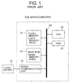
- Fig. 1 shows a block diagram for the rewriting of data in a flash memory.
- a microcomputer 10A incorporating therein a flash memory 13 is connected to a flash writer 12 disposed outside the microcomputer 10A.
- the microcomputer 10A includes, in addition to the flash memory 13 having a user memory area, a mask ROM 14 storing a specified program for rewriting the data in the flash memory 13, a serial communication unit 15 for serially communicating the microcomputer 10A with the flash writer 12, a CPU 16 for executing the programs in the flash memory 13 and the mask ROM 14, and a RAM 17 for temporarily storing data therein.
- These components are connected to each other via an internal bus 19 installed in the microcomputer 10A.
- Fig. 2 is a flowchart showing the processing in rewriting the flash memory of Fig. 1.
- the flash writer 12 transmits/receives information necessary for rewriting the contents stored in the user memory area of the flash memory 13, to/from the microcomputer 10A via the serial communication unit 15.
- the flash writer 12 makes predetermined operations to set the CPU 16 to a flash programming mode (step S21), and then transmits parameters including programming and erasing voltages and programming and erasing times (step S22) for the rewriting.
- the microcomputer 10A executes the program (flash firmware) stored in the mask memory area of the mask ROM 14, thereby starting the process for rewriting the user memory area (step S23).
- the flash writer 12 transmits data for updating the data in the user memory area.
- the microcomputer 10A rewrites this data into the user memory area.
- a user who operates the flash writer 12 recognizes the type and version of the flash memory 13 from the stamp information printed on the microcomputer 10A, and selects the parameters, such as programming voltage and programming time that are considered to be optimal for rewriting the flash memory 13.
- the version information of the microcomputer can be printed thereon, and not the lot information during fabrication (i.e., information about differences in characteristics resulting from variations of process conditions during fabrication).
- the mask ROM 13 may store some parameters, in which case some burden to the user can be alleviated.
- flash memories 13 of the same type and the same version often vary in optimum programming voltage, programming time, and so on from one fabrication lot to another.
- the use of the parameters selected by the user based on the stamp information alone and the use of the default parameters provide no guarantee that the user memory area is rewritten under the optimum conditions.
- the present invention provides a microcomputer unit comprising a flash memory for storing specified data, a ROM storing a program for rewriting the specified data stored in the flash memory, a nonvolatile memory for storing version information and/or lot information of the flash memory, and a CPU for responding to an external command to execute the program for rewriting the specified data in the flash memory based on the version information and/or lot information stored in the nonvolatile memory.
- the present invention also provides a method for rewriting data stored in a flash memory installed in a microcomputer by using a CPU, the method comprising the steps of:
- whether or not the rewrite control program and parameters stored in the mask ROM are available for the rewrite processing for the flash memory is determined based on the version information and/or lot information read from the nonvolatile memory.
- the rewrite processing to the flash memory is executed under the optimum conditions, whereby the rewrite processing improves in reliability and efficiency.
- the microcomputer 10 includes, in addition to the flash memory 13, a mask ROM 14, a serial communication unit 15, a CPU 16, a RAM 7, and a nonvolatile memory 18. All these components are connected to an internal bus 19.
- the flash memory 13 has a user memory area of e.g. 1 Mbyte, into which programs according to user applications are stored.
- the mask ROM 14 has a mask memory area of e.g. 8 Kbytes, and stores flash firmware for performing write control conducted to the flash memory 13. Besides, the mask ROM 14 stores default parameters indicating the programming voltage, programming time, and other parameters necessary for the write control, and flash identification information which identifies the type, version, lot information etc. of the flash memory 13.
- the serial communication unit 15 is implemented as a serial or parallel interface. The serial communication unit 15 transmits/receives information necessary for the write control to/from the flash writer 12 disposed outside the microcomputer 10.
- the CPU 16 is connected via the internal bus 19 to the functional units including the flash memory 13, the mask ROM 14, the serial communication unit 15, the RAM 17, and the nonvolatile memory 18.
- the CPU 16 executes write/read operations to the individual functional units.
- the nonvolatile memory 18 stores updated flash firmware or parameters, and version information indicating whether or not an update is made to the flash firmware or parameters.
- Fig. 4 there is shown a flowchart of the procedure in rewriting the flash memory of Fig. 3.
- the flash writer 12 maintains the source terminal Vpp of the microcomputer 10 at high voltage, thereby resetting the microcomputer 10 to effect a flash programming mode (step S11).
- the flash writer 2 is capable of transmitting/receiving necessary data to/from the microcomputer 10 via the serial communication unit 15.
- the flash writer 12 initially reads the version information and the flash identification information (step S12).
- the flash writer 12 stores therein information for the types, versions and lots of the flash memories, and thus can determine the program version and parameters optimum to the flash-memory rewrite processing based on the flash identification information.
- the flash writer 12 determines whether or not the flash firmware stored in the mask ROM 14 or the nonvolatile memory 18 is optimum for the rewriting of the flash memory 13 (step S13), and if "YES,” proceeds to step S15. If "NO,” the flash writer 2 transmits the update information including the optimum flash firm and the version information of the flash firm stored in the flash writer 12. The update information is thereby stored into a rewriting memory area of the nonvolatile memory 18 (step S14). It is to be noted that modified portions of the flash firmware instead may be stored exclusively.
- the flash writer 12 determines whether or not the parameters stored in the mask ROM 14 or the nonvolatile memory 18 are optimum for the rewriting of the flash memory 13 based on their version information and the flash identification information (step S15). If “YES,” the process advances to step S17. If “NO,” the flash writer 12 transmits the update information including the optimum parameters and the version information of the parameters. The update information is thereby stored into the rewriting memory area of the nonvolatile memory 18 (step S16).
- the flash writer 12 transmits a command for starting the processing for rewriting the user memory area.
- the CPU 16 upon receiving this command, refers to the version information of the flash firmware and parameters in the rewriting memory area of the nonvolatile memory 18. If there is update information stored, the CPU 16 selects the flash firmware or parameters including the update information in the rewriting memory area. Otherwise, the CPU 16 selects the default flash firmware or parameters in the mask memory area. Based on the request from the CPU 16, the flash writer 12 transmits data to be stored into the user memory area. The CPU 16 executes the selected flash firmware to rewrite the data in the user memory area with the data from the flash writer 12 in accordance with the parameters selected (step S17).
- the optimum value of the voltage Vpp to be used for the write processing varies, for example, from 10.0 V to 10.3 V or so.
- the optimum value of the programming time for 1-byte data varies from 50 ⁇ s to 200 ⁇ s or so.
- the characteristics of flash memories include optimum values that vary from one lot to another due to variations of thicknesses of the gate oxide films and the impurity concentrations in the channels of the transistors constituting the flash memory cells. Thus, flash memories after fabrication are tested for the characteristics thereof.
- the flash writer 12 manages the results of the characteristic tests on the flash memories corresponding to the flash identification information, and stores the optimum conditions for the flash memory writing processing lot by lot.
- the flash identification information is read and used to determine availability of the firmware to the flash memory so that minimum and sufficient items of the flash rewrite control information stored in the microcomputer are rewritten.
- the rewrite processing to the flash memory is performed under the optimum conditions.
- microcomputers and the method of rewriting data in a flash memory according to the present invention are, however, not limited to the configurations of the embodiment described above: Microcomputers and methods of rewriting data in a flash memory obtained through various changes and modifications to the configuration of the embodiment described above also fall within the scope of the present invention.
Landscapes
- Engineering & Computer Science (AREA)
- Theoretical Computer Science (AREA)
- General Engineering & Computer Science (AREA)
- Software Systems (AREA)
- Computer Hardware Design (AREA)
- Physics & Mathematics (AREA)
- General Physics & Mathematics (AREA)
- Computer Security & Cryptography (AREA)
- Computing Systems (AREA)
- Microelectronics & Electronic Packaging (AREA)
- Stored Programmes (AREA)
- Read Only Memory (AREA)
- Microcomputers (AREA)
- Techniques For Improving Reliability Of Storages (AREA)
Abstract
A microcomputer (10) stores a program in a ROM
(14) for rewriting the program stored in a flash memory
(13), and also stores in a nonvolatile memory (18)
parameters to be used for the rewriting, as well as
version information and lot information of the flash
memory (13). A flash writer (12) selects a corrected
program based on the version information, wherein a
CPU (16) executes the corrected program while using the
parameters stored in the nonvolatile memory (18) and the
parameters selected based on the lot information.
Description
- The present invention relates to a microcomputer and a method for rewriting data on a flash memory and, more particularly, to a rewrite control technique for rewriting the contents stored in a flash memory such as mounted on a single chip microcomputer.
- A single chip microcomputer (hereinafter, simply referred to as microcomputer) generally has a plurality of system functions for the sake of responding to a variety of market needs. In a microcomputer, a selected one of a plurality of different programs is stored in a memory for specifying one of the plurality of system functions. The memories installed for storing programs include flash memories which are electrically programmable and erasable. Microcomputer vendors provide users with the environment for writing a user-application-specific program so that the users can rewrite the contents of the program in the flash memory based on various modifications to the specifications.
- Fig. 1 shows a block diagram for the rewriting of data in a flash memory. In the flash memory rewriting, a
microcomputer 10A incorporating therein aflash memory 13 is connected to aflash writer 12 disposed outside themicrocomputer 10A. Themicrocomputer 10A includes, in addition to theflash memory 13 having a user memory area, amask ROM 14 storing a specified program for rewriting the data in theflash memory 13, aserial communication unit 15 for serially communicating themicrocomputer 10A with theflash writer 12, aCPU 16 for executing the programs in theflash memory 13 and themask ROM 14, and aRAM 17 for temporarily storing data therein. These components are connected to each other via aninternal bus 19 installed in themicrocomputer 10A. - Fig. 2 is a flowchart showing the processing in rewriting the flash memory of Fig. 1. The
flash writer 12 transmits/receives information necessary for rewriting the contents stored in the user memory area of theflash memory 13, to/from themicrocomputer 10A via theserial communication unit 15. Theflash writer 12 makes predetermined operations to set theCPU 16 to a flash programming mode (step S21), and then transmits parameters including programming and erasing voltages and programming and erasing times (step S22) for the rewriting. Based on the parameters received, themicrocomputer 10A executes the program (flash firmware) stored in the mask memory area of themask ROM 14, thereby starting the process for rewriting the user memory area (step S23). Theflash writer 12 transmits data for updating the data in the user memory area. Themicrocomputer 10A rewrites this data into the user memory area. - A user who operates the
flash writer 12 recognizes the type and version of theflash memory 13 from the stamp information printed on themicrocomputer 10A, and selects the parameters, such as programming voltage and programming time that are considered to be optimal for rewriting theflash memory 13. - In the above procedure, due to the limitation of the area for the stamp information to be printed thereon, it is usual that the version information of the microcomputer can be printed thereon, and not the lot information during fabrication (i.e., information about differences in characteristics resulting from variations of process conditions during fabrication).
- Instead of the control of setting all the parameters from the flash writer, the
mask ROM 13 may store some parameters, in which case some burden to the user can be alleviated. - Because of variations in the process conditions during fabrication,
flash memories 13 of the same type and the same version often vary in optimum programming voltage, programming time, and so on from one fabrication lot to another. Thus, the use of the parameters selected by the user based on the stamp information alone and the use of the default parameters provide no guarantee that the user memory area is rewritten under the optimum conditions. Moreover, there is a further problem of misreading the version information printed on themicrocomputer 10A. - It is an object of the present invention to solve the foregoing problems in the conventional technique for rewriting the flash memory, and to provide a microcomputer and a method of rewriting data in a flash memory in which the rewriting for the flash memory is performed under optimum conditions.
- The present invention provides a microcomputer unit comprising a flash memory for storing specified data, a ROM storing a program for rewriting the specified data stored in the flash memory, a nonvolatile memory for storing version information and/or lot information of the flash memory, and a CPU for responding to an external command to execute the program for rewriting the specified data in the flash memory based on the version information and/or lot information stored in the nonvolatile memory.
- The present invention also provides a method for rewriting data stored in a flash memory installed in a microcomputer by using a CPU, the method comprising the steps of:
- storing in the microcomputer a first program for rewriting the data stored in the flash memory;
- storing version information and/or lot information of the flash memory in the microcomputer;
- determining parameters for the rewriting based on the version information and/or lot information; and
- running the first program on the CPU to rewrite the data in the flash memory based on the parameters.
-
- In accordance with the microcomputer and the method of rewriting data in a flash memory of the present invention, whether or not the rewrite control program and parameters stored in the mask ROM are available for the rewrite processing for the flash memory is determined based on the version information and/or lot information read from the nonvolatile memory. Thus, the rewrite processing to the flash memory is executed under the optimum conditions, whereby the rewrite processing improves in reliability and efficiency.
-
- Fig. 1 is a block diagram showing the conventional rewriting of data in a flash memory of a microcomputer;
- Fig. 2 is a flowchart showing the processing in the conventional rewriting in the flash memory of Fig. 1.
- Fig. 3 is a block diagram of a flash writer and a microcomputer including a flash memory to be rewritten, showing a rewrite control process according to an embodiment of the present invention; and
- Fig. 4 is a flowchart showing the processing in rewriting of the flash memory shown in Fig. 2.
-
- Hereinafter, in conjunction with the embodiment of the present invention and with reference to the drawings, description will be given of a microcomputer and a method of rewriting data in a flash memory according to an embodiment of the present invention.
- Referring to Fig. 3, there is shown a
flash writer 12 and amicrocomputer 10 including aflash memory 13 to be written, wherein a rewrite control operation is executed according to an embodiment of the present invention. Themicrocomputer 10 includes, in addition to theflash memory 13, amask ROM 14, aserial communication unit 15, aCPU 16, a RAM 7, and anonvolatile memory 18. All these components are connected to aninternal bus 19. - The
flash memory 13 has a user memory area of e.g. 1 Mbyte, into which programs according to user applications are stored. Themask ROM 14 has a mask memory area of e.g. 8 Kbytes, and stores flash firmware for performing write control conducted to theflash memory 13. Besides, themask ROM 14 stores default parameters indicating the programming voltage, programming time, and other parameters necessary for the write control, and flash identification information which identifies the type, version, lot information etc. of theflash memory 13. Theserial communication unit 15 is implemented as a serial or parallel interface. Theserial communication unit 15 transmits/receives information necessary for the write control to/from theflash writer 12 disposed outside themicrocomputer 10. - The
CPU 16 is connected via theinternal bus 19 to the functional units including theflash memory 13, themask ROM 14, theserial communication unit 15, theRAM 17, and thenonvolatile memory 18. TheCPU 16 executes write/read operations to the individual functional units. Thenonvolatile memory 18 stores updated flash firmware or parameters, and version information indicating whether or not an update is made to the flash firmware or parameters. - Referring to Fig. 4, there is shown a flowchart of the procedure in rewriting the flash memory of Fig. 3. The
flash writer 12 maintains the source terminal Vpp of themicrocomputer 10 at high voltage, thereby resetting themicrocomputer 10 to effect a flash programming mode (step S11). After the resetting, the flash writer 2 is capable of transmitting/receiving necessary data to/from themicrocomputer 10 via theserial communication unit 15. - The
flash writer 12 initially reads the version information and the flash identification information (step S12). Theflash writer 12 stores therein information for the types, versions and lots of the flash memories, and thus can determine the program version and parameters optimum to the flash-memory rewrite processing based on the flash identification information. - The
flash writer 12 determines whether or not the flash firmware stored in themask ROM 14 or thenonvolatile memory 18 is optimum for the rewriting of the flash memory 13 (step S13), and if "YES," proceeds to step S15. If "NO," the flash writer 2 transmits the update information including the optimum flash firm and the version information of the flash firm stored in theflash writer 12. The update information is thereby stored into a rewriting memory area of the nonvolatile memory 18 (step S14). It is to be noted that modified portions of the flash firmware instead may be stored exclusively. - The
flash writer 12 then determines whether or not the parameters stored in themask ROM 14 or thenonvolatile memory 18 are optimum for the rewriting of theflash memory 13 based on their version information and the flash identification information (step S15). If "YES," the process advances to step S17. If "NO," theflash writer 12 transmits the update information including the optimum parameters and the version information of the parameters. The update information is thereby stored into the rewriting memory area of the nonvolatile memory 18 (step S16). - The
flash writer 12 then transmits a command for starting the processing for rewriting the user memory area. TheCPU 16, upon receiving this command, refers to the version information of the flash firmware and parameters in the rewriting memory area of thenonvolatile memory 18. If there is update information stored, theCPU 16 selects the flash firmware or parameters including the update information in the rewriting memory area. Otherwise, theCPU 16 selects the default flash firmware or parameters in the mask memory area. Based on the request from theCPU 16, theflash writer 12 transmits data to be stored into the user memory area. TheCPU 16 executes the selected flash firmware to rewrite the data in the user memory area with the data from theflash writer 12 in accordance with the parameters selected (step S17). - The optimum value of the voltage Vpp to be used for the write processing varies, for example, from 10.0 V to 10.3 V or so. The optimum value of the programming time for 1-byte data varies from 50 µ s to 200 µ s or so. The characteristics of flash memories include optimum values that vary from one lot to another due to variations of thicknesses of the gate oxide films and the impurity concentrations in the channels of the transistors constituting the flash memory cells. Thus, flash memories after fabrication are tested for the characteristics thereof. The
flash writer 12 manages the results of the characteristic tests on the flash memories corresponding to the flash identification information, and stores the optimum conditions for the flash memory writing processing lot by lot. - According to the above-described embodiment, the flash identification information is read and used to determine availability of the firmware to the flash memory so that minimum and sufficient items of the flash rewrite control information stored in the microcomputer are rewritten. Thus, the rewrite processing to the flash memory is performed under the optimum conditions.
- The present invention has been described heretofore in conjunction with the preferred embodiment thereof. The microcomputer and the method of rewriting data in a flash memory according to the present invention are, however, not limited to the configurations of the embodiment described above: Microcomputers and methods of rewriting data in a flash memory obtained through various changes and modifications to the configuration of the embodiment described above also fall within the scope of the present invention.
Claims (6)
- A microcomputer unit comprising a flash memory (13) for storing specified data, a ROM (14) storing a program for rewriting the specified data stored in said flash memory (13), and a CPU (16) for responding to an external command to execute the program for rewriting the specified data in said flash memory (13), characterized in that a nonvolatile memory (18) stores version information and/or lot information of said flash memory (13), and said CPU (16) rewrites the data in said flash memory (13) based on the version information and/or lot information.
- The microcomputer unit as defined in claim 1, wherein said nonvolatile memory (13) has a memory area to be used for storing parameters in the rewriting of the data in said flash memory (13) by said CPU (16).
- The microcomputer unit as defined in claim 1, wherein said nonvolatile memory (18) has a memory area to be used for storing at least a part of a corrected program corrected from the program stored in said ROM (14).
- A method for rewriting data stored in a flash memory installed in a microcomputer by using a CPU, the method comprising the steps of:storing in the microcomputer (10) a first program for rewriting the data stored in the flash memory (13);storing version information and/or lot information of the flash memory (13) in the microcomputer (10);determining parameters for the rewriting based on the version information and/or lot information; andrunning the first program on the CPU (16) to rewrite the data in the flash memory (13) based on the parameters.
- The method as defined in claim 4, wherein the storing step stores the information in a nonvolatile memory (18).
- The method as defined in claim 4, further comprising the steps of selecting a second program among a plurality of programs based on the version information and/or the lot information, and running the second program instead of the first program on said CPU (16).
Applications Claiming Priority (2)
| Application Number | Priority Date | Filing Date | Title |
|---|---|---|---|
| JP2000117963 | 2000-04-19 | ||
| JP2000117963A JP2001306543A (en) | 2000-04-19 | 2000-04-19 | Microcomputer, and data reloading method for flash memory |
Publications (1)
| Publication Number | Publication Date |
|---|---|
| EP1152344A2 true EP1152344A2 (en) | 2001-11-07 |
Family
ID=18629194
Family Applications (1)
| Application Number | Title | Priority Date | Filing Date |
|---|---|---|---|
| EP01250136A Withdrawn EP1152344A2 (en) | 2000-04-19 | 2001-04-18 | Microcomputer and method for rewriting data on flash memory |
Country Status (4)
| Country | Link |
|---|---|
| US (1) | US20020059569A1 (en) |
| EP (1) | EP1152344A2 (en) |
| JP (1) | JP2001306543A (en) |
| KR (1) | KR100425229B1 (en) |
Families Citing this family (13)
| Publication number | Priority date | Publication date | Assignee | Title |
|---|---|---|---|---|
| JP4136359B2 (en) * | 2001-11-15 | 2008-08-20 | 株式会社ルネサステクノロジ | Microcomputer |
| JP2006066009A (en) | 2004-08-30 | 2006-03-09 | Renesas Technology Corp | Semiconductor integrated circuit |
| WO2006025091A1 (en) | 2004-08-30 | 2006-03-09 | Renesas Technology Corp. | Semiconductor integrated circuit |
| TW200632736A (en) * | 2005-03-11 | 2006-09-16 | Ulead Systems Inc | Rewritable medium, management method thereof, and related device |
| CN101030185B (en) * | 2006-02-28 | 2010-05-12 | 鸿富锦精密工业(深圳)有限公司 | USB-to-serial cable update device |
| US7809900B2 (en) * | 2006-11-24 | 2010-10-05 | Sandforce, Inc. | System, method, and computer program product for delaying an operation that reduces a lifetime of memory |
| US7747813B2 (en) * | 2006-11-24 | 2010-06-29 | Sandforce, Inc. | Multi-memory device system and method for managing a lifetime thereof |
| US7904619B2 (en) | 2006-11-24 | 2011-03-08 | Sandforce, Inc. | System, method, and computer program product for reducing memory write operations using difference information |
| US7904672B2 (en) | 2006-12-08 | 2011-03-08 | Sandforce, Inc. | System and method for providing data redundancy after reducing memory writes |
| US7903486B2 (en) | 2007-11-19 | 2011-03-08 | Sandforce, Inc. | System, method, and computer program product for increasing a lifetime of a plurality of blocks of memory |
| US7849275B2 (en) * | 2007-11-19 | 2010-12-07 | Sandforce, Inc. | System, method and a computer program product for writing data to different storage devices based on write frequency |
| JP5226383B2 (en) * | 2008-05-21 | 2013-07-03 | ルネサスエレクトロニクス株式会社 | Microcomputer identification information management system and method |
| US8516166B2 (en) * | 2009-07-20 | 2013-08-20 | Lsi Corporation | System, method, and computer program product for reducing a rate of data transfer to at least a portion of memory |
Family Cites Families (11)
| Publication number | Priority date | Publication date | Assignee | Title |
|---|---|---|---|---|
| US5870520A (en) * | 1992-12-23 | 1999-02-09 | Packard Bell Nec | Flash disaster recovery ROM and utility to reprogram multiple ROMS |
| US5574926A (en) * | 1993-03-11 | 1996-11-12 | Olympus Optical Co., Ltd. | One-chip microcomputer system having function for substantially correcting contents of program |
| US5828911A (en) * | 1993-05-24 | 1998-10-27 | Olympus Optical Co., Ltd. | One chip microcomputer built-in system |
| US5701492A (en) * | 1996-03-29 | 1997-12-23 | Canon Kabushiki Kaisha | Fail-safe flashing of EPROM |
| US6308325B1 (en) * | 1996-04-09 | 2001-10-23 | International Business Machines Corporation | Apparatus and method for downloading data to electronic device |
| WO1998024021A1 (en) * | 1996-11-29 | 1998-06-04 | Hitachi, Ltd. | Microcomputer control system |
| US6041319A (en) * | 1997-07-14 | 2000-03-21 | Pitney Bowes Inc. | Method and system for telephone updates of postal scales |
| JP2914360B2 (en) * | 1997-09-30 | 1999-06-28 | ソニー株式会社 | External storage device and data processing method |
| US6009520A (en) * | 1997-12-10 | 1999-12-28 | Phoenix Technologies, Ltd | Method and apparatus standardizing use of non-volatile memory within a BIOS-ROM |
| US6243809B1 (en) * | 1998-04-30 | 2001-06-05 | Compaq Computer Corporation | Method of flash programming or reading a ROM of a computer system independently of its operating system |
| KR100284430B1 (en) * | 1998-12-18 | 2001-04-02 | 구자홍 | Program update method and device |
-
2000
- 2000-04-19 JP JP2000117963A patent/JP2001306543A/en active Pending
-
2001
- 2001-04-17 US US09/835,641 patent/US20020059569A1/en not_active Abandoned
- 2001-04-18 KR KR10-2001-0020661A patent/KR100425229B1/en not_active Expired - Fee Related
- 2001-04-18 EP EP01250136A patent/EP1152344A2/en not_active Withdrawn
Also Published As
| Publication number | Publication date |
|---|---|
| JP2001306543A (en) | 2001-11-02 |
| US20020059569A1 (en) | 2002-05-16 |
| KR100425229B1 (en) | 2004-03-30 |
| KR20010098686A (en) | 2001-11-08 |
Similar Documents
| Publication | Publication Date | Title |
|---|---|---|
| US6745278B2 (en) | Computer capable of rewriting an area of a non-volatile memory with a boot program during self mode operation of the computer | |
| EP1152344A2 (en) | Microcomputer and method for rewriting data on flash memory | |
| JPH08202626A (en) | Memory controller | |
| US20020039312A1 (en) | Nonvolatile memory and method of writing data thereto | |
| US7992009B2 (en) | Device and method capable of verifying program operation of non-volatile memory and method card including the same | |
| JP2006085895A (en) | Program method for nonvolatile memory device having high reliability | |
| CN104969181A (en) | Replacement of a corrupt driver variable record | |
| JP2000187992A (en) | Refresh control circuit for electrically rewritable nonvolatile memory | |
| US7096351B2 (en) | Single-chip microcomputer and boot region switching method thereof | |
| US20110016274A1 (en) | Portable electronic device, smartcard and control method for portable electronic device | |
| US6286757B1 (en) | Portable electronic apparatus | |
| US20110145484A1 (en) | Exhaustive Parameter Search Algorithm for Interface with Nand Flash Memory | |
| US6941413B2 (en) | Nonvolatile memory, its data updating method, and card reader equipped with such nonvolatile memory | |
| KR100310486B1 (en) | Microcumputer | |
| US20050188148A1 (en) | Data access controlling method in flash memory and data access controlling program | |
| JP4826232B2 (en) | Information processing apparatus and boot program rewriting method | |
| US7346730B2 (en) | Mobile electronic device | |
| JP2004310268A (en) | Semiconductor device with built-in flash memory, control method for flash memory, and program for the method | |
| JP2002150246A (en) | Portable electronic devices | |
| JP2000243093A (en) | Data storing method for flash memory and data reading out method from flash memory | |
| US20090077445A1 (en) | Nonvolatile storage device, controller of nonvolatile memory, and nonvolatile storage system | |
| JPH0512511A (en) | Method of changing IC card and its application program | |
| JP2003203211A (en) | Portable electronic devices | |
| US20060136711A1 (en) | Disk device using disk to rewrite firmware and firmware determination method | |
| JP2713583B2 (en) | Electronics |
Legal Events
| Date | Code | Title | Description |
|---|---|---|---|
| PUAI | Public reference made under article 153(3) epc to a published international application that has entered the european phase |
Free format text: ORIGINAL CODE: 0009012 |
|
| AK | Designated contracting states |
Kind code of ref document: A2 Designated state(s): AT BE CH CY DE DK ES FI FR GB GR IE IT LI LU MC NL PT SE TR |
|
| AX | Request for extension of the european patent |
Free format text: AL;LT;LV;MK;RO;SI |
|
| RAP1 | Party data changed (applicant data changed or rights of an application transferred) |
Owner name: NEC ELECTRONICS CORPORATION |
|
| STAA | Information on the status of an ep patent application or granted ep patent |
Free format text: STATUS: THE APPLICATION HAS BEEN WITHDRAWN |
|
| 18W | Application withdrawn |
Effective date: 20050905 |