EP1150432A1 - Successive-approximation analog-digital converter and related operating method - Google Patents
Successive-approximation analog-digital converter and related operating method Download PDFInfo
- Publication number
- EP1150432A1 EP1150432A1 EP00830311A EP00830311A EP1150432A1 EP 1150432 A1 EP1150432 A1 EP 1150432A1 EP 00830311 A EP00830311 A EP 00830311A EP 00830311 A EP00830311 A EP 00830311A EP 1150432 A1 EP1150432 A1 EP 1150432A1
- Authority
- EP
- European Patent Office
- Prior art keywords
- analog
- digital
- signal
- converter
- control circuit
- Prior art date
- Legal status (The legal status is an assumption and is not a legal conclusion. Google has not performed a legal analysis and makes no representation as to the accuracy of the status listed.)
- Granted
Links
Images

Classifications
-
- H—ELECTRICITY
- H03—ELECTRONIC CIRCUITRY
- H03M—CODING; DECODING; CODE CONVERSION IN GENERAL
- H03M1/00—Analogue/digital conversion; Digital/analogue conversion
- H03M1/06—Continuously compensating for, or preventing, undesired influence of physical parameters
- H03M1/08—Continuously compensating for, or preventing, undesired influence of physical parameters of noise
-
- H—ELECTRICITY
- H03—ELECTRONIC CIRCUITRY
- H03M—CODING; DECODING; CODE CONVERSION IN GENERAL
- H03M1/00—Analogue/digital conversion; Digital/analogue conversion
- H03M1/12—Analogue/digital converters
- H03M1/34—Analogue value compared with reference values
- H03M1/38—Analogue value compared with reference values sequentially only, e.g. successive approximation type
- H03M1/46—Analogue value compared with reference values sequentially only, e.g. successive approximation type with digital/analogue converter for supplying reference values to converter
- H03M1/462—Details of the control circuitry, e.g. of the successive approximation register
Definitions
- the present invention relates to a successive-approximation analog-digital converter.
- analog-digital converters that use a successive approximation technique, that is in which an analog signal is converted into a digital signal at N bits in N clock cycles, is generally known in the technical field.
- the converter basically consists of a comparator, a digital-analog converter (DAC) and a digital control logic.
- the function of the digital control logic is to determine the value of each bit by a sequential mode based on the output of the comparator.
- the cycle of conversion starts by sampling the analog input signal that has to be converted; however if the input signal is slowly variable that is, basically a signal that has a variation less than the least significant bit (LSB) for the duration of a conversion it cannot be sampled.
- LSB least significant bit
- the logic control circuit assumes that the most significant bit (MSB) is 1 and all the other bits 0.
- the digital signal is sent to the DAC which generates an analog signal, for example of 0.5 Vref, where Vref is a reference voltage, which is compared with the analog input signal already sampled. If the output of the comparator is high the digital control logic makes the MSB 1, otherwise if the output of the comparator is low the digital control logic makes the MSB 0. This completes the first step in the approximation sequence. At this point, the value of the most significant bit is known. The approximation sequence continues another time sending a digital signal to the DAC, with the most significant bit at its indicated value, the second bit placed at 1 and all the other bits which have a value 0.
- the object of the present invention is to present a successive-approximation analog-digital converter which overcomes the above mentioned drawback.
- a successive-approximation analog-digital converter comprising a logic control circuit timed by an external clock signal, said control circuit being adapted to produce a digital signal formed of N bits through a second analog-digital conversion in N clock cycles; a digital-analog converter that converts said digital signal sent by said logic circuit to an analog signal; a comparator which compares said analog signal with an analog signal at the input of said analog-digital converter, characterised in that said logic control circuit comprises a register which contains a previous digital signal formed of N bits and obtained from a previous analog digital conversion and said converter comprises a device which enables the increase of said analog signal in output from the digital-analog converter and in input to said comparator by a preset value when the bit of said previous digital signal which corresponds in position to the bit of said digital signal which has to be decided in a clock cycle is a zero.
- the present invention it is possible to make a successive-approximation analog-digital converter which, by the addition of a hysteresis at the DAC output, permits the elimination of the anomalies presented by known successive-approximation analog-digital converters in case of conversion of a slowly variable signal which presents oscillations at the transition threshold between the value of the digital signal and the value of the continuous signal.
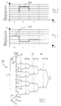
- a successive-approximation analog-digital converter is shown in which a logic control circuit 1 generates the digital signal D in input to a digital-analog converter (DAC) 2.
- DAC digital-analog converter
- the latter generates an analog signal A in input to a comparator 3 at its negative terminal; the comparator 3 compares said analog signal A with an analog signal B which represents the analog signal to convert that has already been sampled.
- the control circuit 1 is a timed logic control circuit as an external clock timing signal acts on it.
- a switch 4 is provided which switches between the two possible states 5 and 6 so that the analog voltage signal A in input to the comparator 3 is or the signal in output from the DAC 2 (in said case the switch 4 is in state 5), or the signal in output from the DAC 2 increased by a low value of voltage Voffs (with the switch 4 in the state 6).
- the switch 4 is controlled by a signal C coming from a control circuit 20 being part of the logic control circuit 1.
- a logic control circuit 1 for a successive-approximation analog-digital converter comprises an outputs register 11 and a digital circuit 12 on which the external clock signals act, start (start of conversion) and end (end of conversion), as can be seen in Figure 2.
- the digital circuit 12 controls the register 11 and also the switch 4 given that it comprises also the control circuit 20.
- the latter which has in input a digital signal D1 previously converted and contained in the register 11, makes switch 4 to switch to position 6 only in the case in which in a clock cycle the bit of the digital signal D1 which corresponds in position to the bit of the digital signal D to convert is a zero.
- the digital signal D is formed of bits b0, b1, b2 and the register 11 contains the result of the previous conversion, that is the digital signal D1 formed of bits b0', b1', b2'.
- the logic control circuit 1 assumes that the b0 of the digital signal D is 1 and all the other bits (bits b1 and b2) 0.
- the digital signal D is sent to DAC 2 which generates the analog signal A, for example by 0.5Vref, where Vref is a reference voltage in input at DAC 2.
- bit b0' of the digital signal D1 is 0 the control circuit 20, through the signal C commands the increase of the analog voltage signal A in output from the DAC 2 of the low Voffs voltage, by means of the switch 4 placed in position 6, otherwise if the bit b0' is 1 the analog signal A is left unaltered.
- the analog signal A is compared with the analog signal in input B. If the output of the comparator is high the logic control circuit 1 makes the MSB equal to 1; otherwise, if the output of the comparator is low, the logic control circuit 1 makes the MSB equal to 0. This completes the first stage of the approximation sequence that is a clock cycle. At this point the value of the most significant bit is known.
- the approximation sequence continues once again sending a digital signal D to the DAC, with the most significant bit b0 at its indicated value, the second bit b1 placed at 1 and the bit b2 placed at 0.
- the bit b1' of the digital signal D1 is 0 the analog voltage signal A in output from the DAC 2 is increased by the low voltage Voffs; otherwise if the bit b1' is 1 the analog signal A is left unaltered.
- the comparison between the signal in input B and the signal A if the output of the comparator is high, the second bit is placed at 1, otherwise the second bit is placed at 0.
- the value of the second bit is also known.
- the approximation sequence continues once again sending a digital signal D to the DAC, with the bits b0 and b1 at their indicated values, and the bit b2 placed at 1.
- the bit b2' of the digital word D1 is 0 the analog voltage signal A in output from the DAC 2 is increased by the low Voffs voltage otherwise if the bit b2' is 1 the analog signal A is left unaltered.
- the signal D determines the digital signal out which is the output of the analog-digital converter.
- the increase in the voltage signal A by the low voltage Voffs creates a hysteresis of voltage 200 which enables the elimination of the anomalies presented by the digital analog successive approximation converters known in the case of conversion of a slowly variable signal which presents oscillations at the transition threshold between the value of the digital signal and the value of the contiguous signal.
- said value of the voltage Voffs is less than the value of voltage of conversion of one least significant bit (LSB).
- the circuit 100 of Figure 5 consists of an n channel M1 transistor MOS and of a p channel M2 transistor MOS both controlled by the signal C and by a common resistive string DAC with resistances R and R/2 and switches controlled by signals b0-b2 and b0neg-b2neg which represent the value and the negation of the bit which compose the digital signal D in input to the DAC 2.
- the signal C which is generally high when closing M1 and opening M2, in the case in which the voltage signal A in output to the circuit 100 must be increased by a Voffs voltage, becomes low causing the opening of M1 and the closing of M2. In this latter case, in comparison to the case of a similar and common resistive string DAC, the voltage signal A in output will be increased by Vref/16 which therefore represents the voltage Voffs.
Landscapes
- Engineering & Computer Science (AREA)
- Theoretical Computer Science (AREA)
- Analogue/Digital Conversion (AREA)
Abstract
Description
Claims (8)
- Successive-approximation analog-digital converter comprising a control logic circuit (1) timed by means of an external clock signal (clock), said control circuit (1) being suitable for producing a digital signal (D) formed of N bits by means of an analog-digital conversion in N clock cycles, a digital-analog converter (2) which converts said digital signal (D) sent by said logic circuit (1) to an analog signal (A), a comparator (3) which compares said analog signal (A) with an analog signal (B) which is in input to said analog-digital converter, characterised in that said logic control circuit (1) comprises a register (11) which contains a previous digital signal (D1) formed of N bits and obtained from a previous analog-digital conversion and said converter comprises a device (4, 20) which enables the increase of said analog signal (A) in output from the digital-analog converter (2) and in input to said comparator (3) of a preset value (Voffs) when the bit of said previous digital signal (D1) which corresponds in position to the bit of said digital signal (D) which must be decided in a clock cycle is zero.
- Converter according to claim 1, characterised in that said device (4, 20) comprises a control circuit (20) and a switch (4) which is switchable to two possible states (5, 6) for the addition or not of said preset value (Voffs) to said analog signal (A) by means of said control circuit (20).
- Converter according to claim 1, characterised in that said analog signal (A) in output from the digital analog converter and said analog signal (B) in input to said analog digital converter are voltage signals.
- Converter according to claim 1, characterised in that said preset value (Voffs) is substantially less than the conversion value of a least significant bit (LSB).
- Method for converting an analog signal (B) into a digital signal at N bits in N clock cycles by means of a successive-approximation analog-digital converter, said converter comprising a logic control circuit (1) timed by means of an external clock signal (clock), said control circuit (1) being suitable for producing a digital signal (D) formed of N bits through a second analog-digital conversion in N clock cycles, a digital-analog converter (2) which converts said digital signal (D) sent by said logic circuit (1) to an analog signal (A), a comparator which compares said analog signal (A) with an analog signal (B) which is in input to said analog digital converter, characterised in that said logic control circuit (1) comprising a register (11) which contains a previous digital signal (D1) formed of N bits and obtained from a previous analog-digital conversion and that each of said clock cycles comprises a step in which the analog signal (A) in output from said digital-analog converter (2) and in input to said comparator (3) is increased by a low value (Voffs) if the bit of the previous digital signal (D1) corresponds in position to the bit of the digital signal (D) which must be decided in said clock cycle is zero.
- Method according to claim 5, characterised in that said increase of a low value (Voffs) of said analog signal (A) in output from said digital-analog converter (2) and in input to said comparator (3) is carried out through a device comprising a control circuit (20) and a switch (4) switchable to two possible states (5, 6) for the addition or not of said preset value (Voffs) to said analog signal (A) through said control circuit.
- Method according to claim 5, characterised in that said analog signal (A) in output from the digital-analog converter and said analog signal sampled (B) in input to said analog-digital converter are voltage signals.
- Method according to claim 5, characterised in that said preset value (Voffs) is substantially less than the conversion value of a least significant bit (LSB).
Priority Applications (4)
| Application Number | Priority Date | Filing Date | Title |
|---|---|---|---|
| EP00830311A EP1150432B1 (en) | 2000-04-27 | 2000-04-27 | Successive-approximation analog-digital converter and related operating method |
| DE60015929T DE60015929T2 (en) | 2000-04-27 | 2000-04-27 | Analog-to-digital converter with gradual approximation and corresponding operating method |
| JP2001119402A JP2001358589A (en) | 2000-04-27 | 2001-04-18 | Successive approximation analog-to-digital converter and conversion method |
| US09/838,090 US6498579B2 (en) | 2000-04-27 | 2001-04-18 | Successive-approximation analog-digital converter and related operating method |
Applications Claiming Priority (1)
| Application Number | Priority Date | Filing Date | Title |
|---|---|---|---|
| EP00830311A EP1150432B1 (en) | 2000-04-27 | 2000-04-27 | Successive-approximation analog-digital converter and related operating method |
Publications (2)
| Publication Number | Publication Date |
|---|---|
| EP1150432A1 true EP1150432A1 (en) | 2001-10-31 |
| EP1150432B1 EP1150432B1 (en) | 2004-11-17 |
Family
ID=8175303
Family Applications (1)
| Application Number | Title | Priority Date | Filing Date |
|---|---|---|---|
| EP00830311A Expired - Lifetime EP1150432B1 (en) | 2000-04-27 | 2000-04-27 | Successive-approximation analog-digital converter and related operating method |
Country Status (4)
| Country | Link |
|---|---|
| US (1) | US6498579B2 (en) |
| EP (1) | EP1150432B1 (en) |
| JP (1) | JP2001358589A (en) |
| DE (1) | DE60015929T2 (en) |
Families Citing this family (1)
| Publication number | Priority date | Publication date | Assignee | Title |
|---|---|---|---|---|
| DE10303347B4 (en) * | 2003-01-29 | 2010-04-29 | Eads Deutschland Gmbh | Method and circuit for converting an analog actual signal into a digital desired signal |
Citations (3)
| Publication number | Priority date | Publication date | Assignee | Title |
|---|---|---|---|---|
| DE2119649A1 (en) * | 1971-04-22 | 1972-11-02 | Licentia Patent-Verwaltungs-Gmbh, 6000 Frankfurt | Analog-to-digital converter |
| US4196420A (en) * | 1978-05-30 | 1980-04-01 | National Semiconductor Corporation | Expanded analog-to-digital converter having one-half LSB shift |
| US5119097A (en) * | 1987-08-13 | 1992-06-02 | Nissan Motor Company, Limited | Analog-to-digital converter having decreased reference voltage to reduce display flicker |
Family Cites Families (9)
| Publication number | Priority date | Publication date | Assignee | Title |
|---|---|---|---|---|
| CA2004317C (en) * | 1988-12-07 | 1993-11-30 | Noriyuki Tokuhiro | Successive comparison type analog-to-digital converting apparatus |
| US5184131A (en) * | 1989-07-06 | 1993-02-02 | Nissan Motor Co., Ltd. | A-d converter suitable for fuzzy controller |
| GB9503783D0 (en) * | 1995-02-24 | 1995-04-12 | Fujitsu Ltd | Analog-to-digital converters |
| JPH08256060A (en) * | 1995-03-17 | 1996-10-01 | Nec Corp | Comparative a/d converter |
| JPH10303751A (en) * | 1997-04-22 | 1998-11-13 | Miyagi Oki Denki Kk | Analog/digital converter |
| JPH10336032A (en) * | 1997-05-30 | 1998-12-18 | Mitsubishi Electric Corp | A / D converter |
| KR100268886B1 (en) * | 1998-01-13 | 2000-10-16 | 김영환 | Analog digital converter |
| JP2000134098A (en) * | 1998-10-21 | 2000-05-12 | Mitsubishi Electric Corp | AD converter |
| US6300889B1 (en) * | 2000-06-19 | 2001-10-09 | Cygnal Integrated Products, Inc. | System on chip with ADC having serial test mode |
-
2000
- 2000-04-27 DE DE60015929T patent/DE60015929T2/en not_active Expired - Fee Related
- 2000-04-27 EP EP00830311A patent/EP1150432B1/en not_active Expired - Lifetime
-
2001
- 2001-04-18 JP JP2001119402A patent/JP2001358589A/en active Pending
- 2001-04-18 US US09/838,090 patent/US6498579B2/en not_active Expired - Lifetime
Patent Citations (3)
| Publication number | Priority date | Publication date | Assignee | Title |
|---|---|---|---|---|
| DE2119649A1 (en) * | 1971-04-22 | 1972-11-02 | Licentia Patent-Verwaltungs-Gmbh, 6000 Frankfurt | Analog-to-digital converter |
| US4196420A (en) * | 1978-05-30 | 1980-04-01 | National Semiconductor Corporation | Expanded analog-to-digital converter having one-half LSB shift |
| US5119097A (en) * | 1987-08-13 | 1992-06-02 | Nissan Motor Company, Limited | Analog-to-digital converter having decreased reference voltage to reduce display flicker |
Also Published As
| Publication number | Publication date |
|---|---|
| DE60015929D1 (en) | 2004-12-23 |
| JP2001358589A (en) | 2001-12-26 |
| US6498579B2 (en) | 2002-12-24 |
| US20010038352A1 (en) | 2001-11-08 |
| DE60015929T2 (en) | 2005-12-22 |
| EP1150432B1 (en) | 2004-11-17 |
Similar Documents
| Publication | Publication Date | Title |
|---|---|---|
| EP0401245B1 (en) | Digital to analogue converter | |
| US5028926A (en) | Successive type analog-to-digital converter with a variable reference voltage for the digital to analog converter | |
| US6239734B1 (en) | Apparatus and a method for analog to digital conversion using plural reference signals and comparators | |
| US6844840B1 (en) | Successive-approximation-register (SAR) analog-to-digital converter (ADC) and method utilizing N three-way elements | |
| JP4017805B2 (en) | Method for converting an analog signal into a multi-bit digital representation and an analog / digital converter | |
| US6340943B1 (en) | Analog to digital converter method and apparatus | |
| US5682163A (en) | Semi-pipelined analog-to-digital converter | |
| KR100286326B1 (en) | Interleaving sampling analog/digital converter | |
| US5589832A (en) | Low noise non-sampled successive approximation | |
| KR100268886B1 (en) | Analog digital converter | |
| EP1150432B1 (en) | Successive-approximation analog-digital converter and related operating method | |
| US6154165A (en) | Variable clock rate, variable bit-depth analog-to-digital converter | |
| US6741192B2 (en) | A/D conversion method for serial/parallel A/D converter, and serial/parallel A/D converter | |
| US6816096B2 (en) | Response-based analog-to-digital conversion apparatus and method | |
| WO2024124698A1 (en) | Logic control apparatus and method for analog-to-digital converter and electronic device | |
| KR100447235B1 (en) | Analog to digital converter | |
| EP0164747A2 (en) | Successive approximation adc with variable frequency clock | |
| JPH11251903A (en) | Ad/da conversion sharing circuit | |
| KR100320434B1 (en) | Analog to digital converter | |
| US6927713B2 (en) | Response-based analog-to-digital conversion apparatus and method | |
| KR100339542B1 (en) | High speed a/d converter | |
| JP3461672B2 (en) | Successive approximation A / D converter | |
| KR0116974Y1 (en) | Analog / Digital Inverter | |
| JP2002033661A (en) | Digital-to-analog conversion circuit | |
| KR100189748B1 (en) | A/d converter of high speed consecutive approximation |
Legal Events
| Date | Code | Title | Description |
|---|---|---|---|
| PUAI | Public reference made under article 153(3) epc to a published international application that has entered the european phase |
Free format text: ORIGINAL CODE: 0009012 |
|
| AK | Designated contracting states |
Kind code of ref document: A1 Designated state(s): AT BE CH CY DE DK ES FI FR GB GR IE IT LI LU MC NL PT SE |
|
| AX | Request for extension of the european patent |
Free format text: AL;LT;LV;MK;RO;SI |
|
| 17P | Request for examination filed |
Effective date: 20020404 |
|
| AKX | Designation fees paid |
Free format text: DE FR GB IT |
|
| 17Q | First examination report despatched |
Effective date: 20040203 |
|
| GRAP | Despatch of communication of intention to grant a patent |
Free format text: ORIGINAL CODE: EPIDOSNIGR1 |
|
| GRAS | Grant fee paid |
Free format text: ORIGINAL CODE: EPIDOSNIGR3 |
|
| GRAA | (expected) grant |
Free format text: ORIGINAL CODE: 0009210 |
|
| AK | Designated contracting states |
Kind code of ref document: B1 Designated state(s): DE FR GB IT |
|
| REG | Reference to a national code |
Ref country code: GB Ref legal event code: FG4D |
|
| REF | Corresponds to: |
Ref document number: 60015929 Country of ref document: DE Date of ref document: 20041223 Kind code of ref document: P |
|
| PLBE | No opposition filed within time limit |
Free format text: ORIGINAL CODE: 0009261 |
|
| STAA | Information on the status of an ep patent application or granted ep patent |
Free format text: STATUS: NO OPPOSITION FILED WITHIN TIME LIMIT |
|
| 26N | No opposition filed |
Effective date: 20050818 |
|
| ET | Fr: translation filed | ||
| PGFP | Annual fee paid to national office [announced via postgrant information from national office to epo] |
Ref country code: DE Payment date: 20070327 Year of fee payment: 8 |
|
| PGFP | Annual fee paid to national office [announced via postgrant information from national office to epo] |
Ref country code: IT Payment date: 20070608 Year of fee payment: 8 |
|
| PGFP | Annual fee paid to national office [announced via postgrant information from national office to epo] |
Ref country code: FR Payment date: 20070426 Year of fee payment: 8 |
|
| PG25 | Lapsed in a contracting state [announced via postgrant information from national office to epo] |
Ref country code: DE Free format text: LAPSE BECAUSE OF NON-PAYMENT OF DUE FEES Effective date: 20081101 |
|
| REG | Reference to a national code |
Ref country code: FR Ref legal event code: ST Effective date: 20081231 |
|
| PG25 | Lapsed in a contracting state [announced via postgrant information from national office to epo] |
Ref country code: FR Free format text: LAPSE BECAUSE OF NON-PAYMENT OF DUE FEES Effective date: 20080430 |
|
| PG25 | Lapsed in a contracting state [announced via postgrant information from national office to epo] |
Ref country code: IT Free format text: LAPSE BECAUSE OF NON-PAYMENT OF DUE FEES Effective date: 20080427 |
|
| PGFP | Annual fee paid to national office [announced via postgrant information from national office to epo] |
Ref country code: GB Payment date: 20100329 Year of fee payment: 11 |
|
| GBPC | Gb: european patent ceased through non-payment of renewal fee |
Effective date: 20110427 |
|
| PG25 | Lapsed in a contracting state [announced via postgrant information from national office to epo] |
Ref country code: GB Free format text: LAPSE BECAUSE OF NON-PAYMENT OF DUE FEES Effective date: 20110427 |