EP1150224A2 - Testing simulated chips - Google Patents
Testing simulated chips Download PDFInfo
- Publication number
- EP1150224A2 EP1150224A2 EP01303720A EP01303720A EP1150224A2 EP 1150224 A2 EP1150224 A2 EP 1150224A2 EP 01303720 A EP01303720 A EP 01303720A EP 01303720 A EP01303720 A EP 01303720A EP 1150224 A2 EP1150224 A2 EP 1150224A2
- Authority
- EP
- European Patent Office
- Prior art keywords
- delay
- data slice
- data
- array
- slice
- Prior art date
- Legal status (The legal status is an assumption and is not a legal conclusion. Google has not performed a legal analysis and makes no representation as to the accuracy of the status listed.)
- Withdrawn
Links
Images





Classifications
-
- G—PHYSICS
- G06—COMPUTING OR CALCULATING; COUNTING
- G06F—ELECTRIC DIGITAL DATA PROCESSING
- G06F30/00—Computer-aided design [CAD]
- G06F30/30—Circuit design
- G06F30/32—Circuit design at the digital level
- G06F30/33—Design verification, e.g. functional simulation or model checking
Definitions
- the present invention relates generally to computer architecture and to testing simulated chips. More particularly, but not by way of limitation, it concerns a method and apparatus for testing a simulated integrated circuit chip's response to input propagation delays by emulating delays throughout a tolerance range, and also programmable delay elements for source synchronous link function design verification through simulation.
- Links For example, on a circuit board, integrated circuit (IC) chips may be connected using links, or cables. Data may be sent to a chip in a data slice, or bundle, along with a data strobe. The data strobe is used to indicate that the accompanying data is valid. The recipient latches the data as soon as it sees the strobe.
- the length of these links may create a propagation delay in the transfer of data, which creates a potential problem for the chip receiving the data. This is particularly a problem with synchronous links where the protocol allows a phase of a signal to cross a synchronous boundary.
- a chip may be designed to recognize and properly respond to link delays within a certain, specified tolerance range. In order to ensure that the chip properly processes data from delayed source synchronous links, it is desirable to test the chip's response to these delays. In this testing process, the simulated chip under test is also referred to as the application specific integrated circuit (ASIC).
- the ASIC is simulated at the hardware description level, also called the register transfer level (RTL).
- RTL register transfer level
- a method and apparatus are disclosed for verifying the functional design of a system's response to propagation delays from the inputs of source synchronous links during testing.
- the system emulates propagation delays by receiving data slice from a source, applying a random or known delay to the data slice, and sending the delayed data slice to the chip under test.
- multiple data slices having varying delay values may be used to test combinations of delays.
- a programmable delay element is used to emulate the propagation delays. This is may be implemented at the hardware description level by receiving the data slice onto multiple data buses, applying a different delay to the data slice on each data bus, and sending the delayed data slices as inputs into a multiplexor.
- the multiplexor may have a selector input that determines which amount of delay to test. To test multiple data slices in combination, multiple multiplexors may be used.
- the delay may be emulated using a higher level programming language and creating a multidimensional array.
- the array receives different data slices, and in the other it assigns different delay values.
- the multidimensional array then receives multiple data slices at the same time. Each delay value is stored in a different array location, depending upon the delay assigned to the data slice.
- An output entry is sent to the chip under test.
- the array entries may be shifted each clock cycle to the output entry, or a pointer may be used to specify a different output entry each clock cycle.
- Figure 1 is a block diagram of the system.
- Figure 2 is a more detailed block diagram of the system of Figure 2.
- Figure 3 is a block diagram of a system for testing more than one ASIC.
- Figure 4 is a flow chart of the method used by the system.
- Figure 5 is a block diagram showing a hardware description language implementation of the programmable delay element.
- Figure 6 is a flow chart of one implementation of the method.
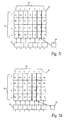
- Figures 7A through 7F show the progression of data slices through a matrix of a second implementation of the programmable delay element.
- the method verifies a chip's functional design with respect to the processing of data slices from source synchronous links by emulating multiple delay values, individually and in combination.
- Programmable delay elements are placed into RTL or C language at the inputs of an RTL ASIC. By so doing, the ASIC(s) under test will see the delay. Because the RTL ASIC drives an ideal edge, the test environment receives only aligned data.
- the system may be implemented to test a bi-directional link by using a delay element for each direction. In a bi-directional test, the input of each delay element is connected to the output of the other.
- the delay elements have independent drive enables controlled by their respective sources.
- FIG. 1 shows a simplified block diagram of the system 10 for emulating the propagation delay of a link for the purpose of testing a chip.
- the system 10 includes a data source 12, which sends data and a data strobe to an ASIC under test 16.
- the data source 12 may be another ASIC or other system tools.
- the data and data strobe pass through a programmable delay element 14, which emulates the propagation delay on a link.
- the programmable delay element 14 receives the data/strobe pair from the source 12, delays the data/strobe pair for a specified number of cycles, and then sends the data/strobe pair to the ASIC 16.
- FIG 2 is a more detailed block diagram of a system 10 for testing an ASIC 16 having two input and two output ports on the left and right sides of the ASIC 16.
- the system 10 has a source 12 that sends a plurality of data slices 18 to the programmable delay element 14.
- the programmable delay element 14 delays the data slices 18 by varying numbers of cycles before sending the data slices 18 to the ASIC 16.
- the ASIC 16 sends a response signal back to the source 12.
- the ASIC 16 is being tested on two input ports on the left and right sides.
- a second source 12' is shown using a second programmable delay element 14'.
- the ASIC 16 sends the response signal back to the second source 12'.
- FIG 3 shows another configuration of the system in which two ASICs 16, 16' are under test. Each ASIC 16, 16' is tested on two input ports. A separate programmable delay element 14, 14', 14", 14"' is used to emulate the propagation delay on each of the links. The output response signal from the first ASIC 16 is sent as an input to the second ASIC 16', showing that the source of data may be another ASIC 16.
- Figure 4 shows a flow chart of the method used to emulate the propagation delay of the links.
- a data slice 18 is received 100 by a programmable delay element 14.
- a random or predetermined delay value is assigned 110 to the data slice 18.
- the programmable delay element emulates 120 the propagation delay, and then sends 130 the delayed data slice to the ASIC 16.
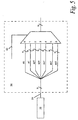
- FIG. 5 illustrates the hardware that may be used in one implementation of the programmable delay element 14.
- the programmable delay element 14 is implemented using a transport delay in hardware description language.
- This implementation shows a source 12 sending a data slice along a bus 24.
- the bus 24 is split into multiple busses, each of which delays the data slice by a different number of cycles, ranging from zero cycles to 6 cycles in the embodiment shown in Figure 5.
- the "#" symbols represent a delay element having a delay of the stated number of cycles.
- These delayed data slices are then input into a multiplexor 20.
- the output of the multiplexor 20 is a delayed data slice that is input into the ASIC 16.
- a selector 22 on the multiplexor 20 controls which input data slice is output, and thus controls the amount of delay on the data slice that is sent to the ASIC 16.
- the user may test combinations of multiple data slices 18 by using multiple multiplexors 20.
- Figure 6 is a flow chart of the method implemented in hardware description language.
- the data slice 18 is received 200 from the source 12 onto a bus 24.
- the bus 24 is split 210 into a number of separate busses.
- a transport delay is then applied 220 to the data slice 18 carried by each separate bus.
- These delayed data slices are then input 230 into the multiplexor 20.
- the desired delay is selected 240 with the selector 22 on the multiplexor 20, which then outputs from the multiplexor 20 the data slice having the desired delay. This output is then sent 250 to the ASIC.
- Figures 7A through 7G show another embodiment using a higher level software design, such as C programming language.
- This implementation of the programmable delay element creates an array 30, which stores the data slices 18.
- the data slices 18 are input into the array 30, they are assigned different delay values 32, depending upon their location in the array 30.
- Figure 7A shows a two-dimensional, 7x4 entry array 30.
- a multidimensional array 30 allows the programmable delay element to process multiple data slices 18 in desired combinations.
- the vertical axis represents different data inputs 18 to the array, and the horizontal axis represents different delay values 32.
- the horizontal position in the example shown in Figure 7A has increasing delay values 32 moving right to left.
- Figure 7B shows the array 30 one clock cycle after the state shown by Figure 7A.
- Four data slices A0, B0, C0, D0 are simultaneously entered into the array 30. These data slices 18 are entered within their respective, predetermined rows in varying horizontal positions representing different delay values 32.
- the array 30 may be named "pipe” and the convention of a particular array location would be given by ' pipe[delay][slice].
- Data slices 18 are entered into the array 30 in a first-in, first-out (FIFO) basis, such that, for example, in an array 30 having seven horizontal spaces, the eighth data slice will overwrite the first, the ninth will overwrite the second, etc.
- FIFO first-in, first-out
- Figure 7C shows the array 30 in the following clock cycle, in which data slices A1, B1, C1, D1 have been inserted into open spaces in the array 30. This addition of new data slices 18 continues for each slice during each cycle, as shown by Figures 7D and 7E.
- Figure 7F shows the entries of the array during the tenth cycle.
- an output slice 30 is sent from the programmable delay element 14 to the ASIC 16.
- the output slice may contain a combination of data slices 18 having various delays 32. This may be implemented by shifting the data horizontally through the array 30 and reading out the rightmost entry, which method is not shown.
- the output method may be implemented using pipe pointers 36 as shown in Figures 7A through 7G. After data slices 18 are entered into the array 30, the pipe pointers 36 shift to the left on the following clock cycle.
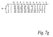
- the output slice 34 tracks the zero pipe pointer 36, as reflected by the bold lines in Figures 7A through 7F showing the output slice 34 at sequential clock cycles.
- Figure 7G is a table showing the output slices 34 for the ten sequential clock cycles represented in Figures 7A through 7F.
- delay values can be determined from inputs to the environment and set at run-time. This provides greater efficiency than existing methods, because recompilation is not required.
- pseudo-random number generator By using a pseudo-random number generator to generate delay values throughout the tolerance range, greater coverage is obtained.
Landscapes
- Engineering & Computer Science (AREA)
- Computer Hardware Design (AREA)
- Physics & Mathematics (AREA)
- Theoretical Computer Science (AREA)
- Evolutionary Computation (AREA)
- Geometry (AREA)
- General Engineering & Computer Science (AREA)
- General Physics & Mathematics (AREA)
- Test And Diagnosis Of Digital Computers (AREA)
- Tests Of Electronic Circuits (AREA)
- Design And Manufacture Of Integrated Circuits (AREA)
Abstract
Description

Claims (10)
- A method for verifying the functional design of a simulated chip (16) receiving data from a link comprising:receiving at a programmable delay element a data slice (18) from a source (12);emulating a link delay using the programmable delay element (14) to delay sending the data slice (18); andsending a delayed data slice (18) to the simulated chip (16) under test.
- The method of claim 1, wherein the programmable delay element (14) comprises a multiplexor (20) capable of receiving a plurality of data slices (18) having different amounts of delay, said multiplexor (20) having a selector input (22) for selecting the desired link delay.
- The method of claims 1 or 2, wherein the step of emulating comprises:assigning the received data slice (18) a delay value;storing the received data slice (18) in an array (30) in a location determined by its assigned delay value, wherein the array (30) is capable of holding a plurality of separate received data slices (18) having various assigned delay values; andwaiting for the duration of the delay value.
- The method of claim 3, wherein the step of emulating further comprises:advancing the received data slice (18) through the array (30) with each advancing clock cycle; andwherein the data slice (30) is sent to the simulated chip (16) under test when the data slice (18) reaches an output entry in the array (30).
- The method of claim 3, wherein the step of emulating further comprises:using a pointer (36) to track the state of the array (30) on each clock cycle;advancing the pointer (36) each clock cycle;writing the data slice (18) to an array (30) entry based upon the location of the pointer (36); andwherein the data slice (18) is sent to the simulated chip (16) under test when the data slice (18) is in an output entry (34) determined by the location of the pointer (36).
- A system for verifying the functional design of a simulated chip (16) receiving data from a link comprising:a data source (12) that sends test data slices (18); anda programmable delay element (14) that receives a data slice (18) from the source (12), applies a time delay to the data slice (18), and sends the delayed data slice (18) to a simulated chip (16) under test, wherein the time delay may be selected from a range.
- The system of claim 6, wherein the programmable delay element (14) receives and processes a plurality of data slices (18) from the source (12).
- The system of claims 6 or 7, wherein the programmable delay element (14) further comprises:a source bus (24) that receives a data slice (18) from the source (12);a plurality of delay buses connected to the source bus (24); anda plurality of delay elements that apply a different delay to the data slice (18) on each of the delay buses to create a plurality of delayed data slices (18).
- The system of claims 6, 7, or 8, wherein the programmable delay element (14) further comprises a multiplexor (20) that receives the plurality of delayed data slices (18) and outputs a data slice (18) having a selected delay.
- The system of claims 6, 7, 8, or 9, wherein the programmable delay element (14) comprises an array (30) that inserts the received data slice (18) into an entry in the array (30) corresponding to the length of the delay, and wherein the data slice (18) is removed from the array (30) and sent to the simulated chip (16) under test.
Applications Claiming Priority (2)
| Application Number | Priority Date | Filing Date | Title |
|---|---|---|---|
| US560191 | 1990-07-31 | ||
| US09/560,191 US6611936B2 (en) | 2000-04-28 | 2000-04-28 | Programmable delay elements for source synchronous link function design verification through simulation |
Publications (2)
| Publication Number | Publication Date |
|---|---|
| EP1150224A2 true EP1150224A2 (en) | 2001-10-31 |
| EP1150224A3 EP1150224A3 (en) | 2003-04-02 |
Family
ID=24236742
Family Applications (1)
| Application Number | Title | Priority Date | Filing Date |
|---|---|---|---|
| EP01303720A Withdrawn EP1150224A3 (en) | 2000-04-28 | 2001-04-24 | Testing simulated chips |
Country Status (3)
| Country | Link |
|---|---|
| US (1) | US6611936B2 (en) |
| EP (1) | EP1150224A3 (en) |
| JP (1) | JP2002024315A (en) |
Cited By (1)
| Publication number | Priority date | Publication date | Assignee | Title |
|---|---|---|---|---|
| US6785832B2 (en) * | 2001-06-22 | 2004-08-31 | International Business Machines Corporation | Process independent source synchronous data capture apparatus and method |
Families Citing this family (16)
| Publication number | Priority date | Publication date | Assignee | Title |
|---|---|---|---|---|
| US6920584B2 (en) * | 2001-11-02 | 2005-07-19 | Sun Microsystems, Inc. | System design verification using selected states of a processor-based system to reveal deficiencies |
| FR2841668B1 (en) * | 2002-06-26 | 2006-08-11 | Emulation And Verification Eng | METHOD AND SYSTEM FOR EMULATING A TEST CIRCUIT ASSOCIATED WITH A TEST ENVIRONMENT |
| US7382824B1 (en) * | 2004-08-13 | 2008-06-03 | Emc Corporaration | Method and apparatus for accurate modeling of multi-domain clock interfaces |
| US20060176096A1 (en) * | 2005-02-10 | 2006-08-10 | International Business Machines Corporation | Power supply insensitive delay element |
| US7355435B2 (en) * | 2005-02-10 | 2008-04-08 | International Business Machines Corporation | On-chip detection of power supply vulnerabilities |
| US7279949B2 (en) * | 2005-02-11 | 2007-10-09 | International Business Machines Corporation | Programmable delay element |
| US7131093B1 (en) | 2006-02-07 | 2006-10-31 | International Business Machines Corporation | Methods and apparatus for creating a programmable link delay |
| US8887045B2 (en) * | 2008-06-11 | 2014-11-11 | Caterpillar Inc. | System and method for providing data links |
| CN102591754A (en) * | 2011-01-18 | 2012-07-18 | 智比特信息技术(镇江)有限公司 | Automatic testing method for electronic product controlled by computer |
| JPWO2012105013A1 (en) * | 2011-02-02 | 2014-07-03 | 富士通株式会社 | Circuit design support device, circuit design support program, and circuit design support method |
| US10095582B2 (en) * | 2014-10-29 | 2018-10-09 | International Business Machines Corporation | Partial rebuilding techniques in a dispersed storage unit |
| US20180181332A1 (en) * | 2014-10-29 | 2018-06-28 | International Business Machines Corporation | Expanding a dispersed storage network memory beyond two locations |
| US10459792B2 (en) * | 2014-10-29 | 2019-10-29 | Pure Storage, Inc. | Using an eventually consistent dispersed memory to implement storage tiers |
| US20180113747A1 (en) * | 2014-10-29 | 2018-04-26 | International Business Machines Corporation | Overdrive mode for distributed storage networks |
| US10223033B2 (en) * | 2014-10-29 | 2019-03-05 | International Business Machines Corporation | Coordinating arrival times of data slices in a dispersed storage network |
| CN112448867B (en) * | 2020-11-26 | 2022-06-21 | 海光信息技术股份有限公司 | Signal delay testing method and device, computer readable storage medium and electronic equipment |
Family Cites Families (18)
| Publication number | Priority date | Publication date | Assignee | Title |
|---|---|---|---|---|
| US5579326A (en) * | 1994-01-31 | 1996-11-26 | Sgs-Thomson Microelectronics, Inc. | Method and apparatus for programming signal timing |
| US5633813A (en) * | 1994-05-04 | 1997-05-27 | Srinivasan; Seshan R. | Apparatus and method for automatic test generation and fault simulation of electronic circuits, based on programmable logic circuits |
| US5862361A (en) * | 1995-09-07 | 1999-01-19 | C.A.E. Plus, Inc. | Sliced synchronous simulation engine for high speed simulation of integrated circuit behavior |
| US5740086A (en) * | 1996-01-11 | 1998-04-14 | Advantest Corp. | Semiconductor test system linked to cad data |
| US6115769A (en) * | 1996-06-28 | 2000-09-05 | Lsi Logic Corporation | Method and apparatus for providing precise circuit delays |
| US5841967A (en) * | 1996-10-17 | 1998-11-24 | Quickturn Design Systems, Inc. | Method and apparatus for design verification using emulation and simulation |
| US6078545A (en) * | 1996-12-26 | 2000-06-20 | Oki Electric Industry Co., Ltd. | Data transfer circuit |
| US6133751A (en) * | 1998-08-05 | 2000-10-17 | Xilinx, Inc. | Programmable delay element |
| US6073194A (en) | 1997-07-31 | 2000-06-06 | Advanced Micro Devices, Inc. | Transaction based windowing methodology for pre-silicon verification |
| US5930482A (en) | 1997-07-31 | 1999-07-27 | Advanced Micro Devices, Inc. | Transaction checking system for verifying bus bridges in multi-master bus systems |
| US5936977A (en) * | 1997-09-17 | 1999-08-10 | Cypress Semiconductor Corp. | Scan path circuitry including a programmable delay circuit |
| US5970052A (en) | 1997-09-19 | 1999-10-19 | International Business Machines Corporation | Method for dynamic bandwidth testing |
| US5936953A (en) * | 1997-12-18 | 1999-08-10 | Raytheon Company | Multi-mode, multi-channel communication bus |
| US6421784B1 (en) * | 1999-03-05 | 2002-07-16 | International Business Machines Corporation | Programmable delay circuit having a fine delay element selectively receives input signal and output signal of coarse delay element |
| US6222407B1 (en) * | 1999-03-05 | 2001-04-24 | International Business Machines Corporation | Dual mode programmable delay element |
| US6397354B1 (en) * | 1999-03-26 | 2002-05-28 | Hewlett-Packard Company | Method and apparatus for providing external access to signals that are internal to an integrated circuit chip package |
| US6378092B1 (en) * | 1999-10-15 | 2002-04-23 | Hewlett-Packard Company | Integrated circuit testing |
| US6348827B1 (en) * | 2000-02-10 | 2002-02-19 | International Business Machines Corporation | Programmable delay element and synchronous DRAM using the same |
-
2000
- 2000-04-28 US US09/560,191 patent/US6611936B2/en not_active Expired - Lifetime
-
2001
- 2001-04-23 JP JP2001124299A patent/JP2002024315A/en active Pending
- 2001-04-24 EP EP01303720A patent/EP1150224A3/en not_active Withdrawn
Cited By (1)
| Publication number | Priority date | Publication date | Assignee | Title |
|---|---|---|---|---|
| US6785832B2 (en) * | 2001-06-22 | 2004-08-31 | International Business Machines Corporation | Process independent source synchronous data capture apparatus and method |
Also Published As
| Publication number | Publication date |
|---|---|
| EP1150224A3 (en) | 2003-04-02 |
| US6611936B2 (en) | 2003-08-26 |
| US20030106005A1 (en) | 2003-06-05 |
| JP2002024315A (en) | 2002-01-25 |
Similar Documents
| Publication | Publication Date | Title |
|---|---|---|
| EP1150224A2 (en) | Testing simulated chips | |
| KR100483636B1 (en) | Method and apparatus for design verification using emulation and simulation | |
| US6810442B1 (en) | Memory mapping system and method | |
| US7512728B2 (en) | Inter-chip communication system | |
| JP4125675B2 (en) | Glitch-free logic system and method insensitive to timing | |
| US7984400B2 (en) | Techniques for use with automated circuit design and simulations | |
| EP0096176B1 (en) | Method of logic simulation and logic simulation machine | |
| US5937179A (en) | Integrated circuit design system with shared hardware accelerator and processes of designing integrated circuits | |
| US20080313579A1 (en) | Techniques For Use With Automated Circuit Design and Simulations | |
| US20010010036A1 (en) | Logic analysis system for logic emulation systems | |
| WO2003077078A2 (en) | Hub array system and method | |
| KR100928134B1 (en) | Custom DCC Systems and Methods | |
| US9069918B2 (en) | System and method implementing full-rate writes for simulation acceleration | |
| GB2131211A (en) | Logic simulator apparatus | |
| GB2401446A (en) | Simulating clock drift between asynchronous clock domains | |
| US7516430B2 (en) | Generating testcases based on numbers of testcases previously generated | |
| Schirner et al. | Result-oriented modeling—A novel technique for fast and accurate TLM | |
| US6075936A (en) | Logic circuit simulation apparatus having cycle-based simulator for simulating circuits including multi-cycle paths | |
| Kim et al. | TPartition: testbench partitioning for hardware-accelerated functional verification | |
| US10210294B1 (en) | System and methods for simulating a circuit design | |
| US7464017B2 (en) | Time multiplexed interface for emulator system | |
| EP1226526A2 (en) | An emulation system having a efficient emulation signal routing architecture | |
| WO2005041074A1 (en) | System and method for functional verification of an electronic integrated circuit design | |
| Naal et al. | High level synthesis methodology for on-line testability optimization | |
| Kanopoulos et al. | Rapid system prototyping using silicon compilation |
Legal Events
| Date | Code | Title | Description |
|---|---|---|---|
| PUAI | Public reference made under article 153(3) epc to a published international application that has entered the european phase |
Free format text: ORIGINAL CODE: 0009012 |
|
| AK | Designated contracting states |
Kind code of ref document: A2 Designated state(s): AT BE CH CY DE DK ES FI FR GB GR IE IT LI LU MC NL PT SE TR |
|
| AX | Request for extension of the european patent |
Free format text: AL;LT;LV;MK;RO;SI |
|
| PUAL | Search report despatched |
Free format text: ORIGINAL CODE: 0009013 |
|
| AK | Designated contracting states |
Kind code of ref document: A3 Designated state(s): AT BE CH CY DE DK ES FI FR GB GR IE IT LI LU MC NL PT SE TR Designated state(s): AT BE CH CY DE DK ES FI FR GB GR IE IT LI LU MC NL PT SE TR |
|
| AX | Request for extension of the european patent |
Extension state: AL LT LV MK RO SI |
|
| 17P | Request for examination filed |
Effective date: 20030926 |
|
| AKX | Designation fees paid |
Designated state(s): DE FR GB |
|
| STAA | Information on the status of an ep patent application or granted ep patent |
Free format text: STATUS: THE APPLICATION IS DEEMED TO BE WITHDRAWN |
|
| 18D | Application deemed to be withdrawn |
Effective date: 20090526 |