EP1148555A1 - RESURF LDMOS field-effect transistor - Google Patents
RESURF LDMOS field-effect transistor Download PDFInfo
- Publication number
- EP1148555A1 EP1148555A1 EP00830308A EP00830308A EP1148555A1 EP 1148555 A1 EP1148555 A1 EP 1148555A1 EP 00830308 A EP00830308 A EP 00830308A EP 00830308 A EP00830308 A EP 00830308A EP 1148555 A1 EP1148555 A1 EP 1148555A1
- Authority
- EP
- European Patent Office
- Prior art keywords
- region
- drain
- conductivity
- well
- resurf
- Prior art date
- Legal status (The legal status is an assumption and is not a legal conclusion. Google has not performed a legal analysis and makes no representation as to the accuracy of the status listed.)
- Withdrawn
Links
- 230000005669 field effect Effects 0.000 title description 2
- 210000000746 body region Anatomy 0.000 claims abstract description 15
- 239000000758 substrate Substances 0.000 claims abstract description 11
- 239000004065 semiconductor Substances 0.000 claims abstract description 4
- ZOXJGFHDIHLPTG-UHFFFAOYSA-N Boron Chemical compound [B] ZOXJGFHDIHLPTG-UHFFFAOYSA-N 0.000 claims description 6
- 229910052796 boron Inorganic materials 0.000 claims description 6
- BHEPBYXIRTUNPN-UHFFFAOYSA-N hydridophosphorus(.) (triplet) Chemical compound [PH] BHEPBYXIRTUNPN-UHFFFAOYSA-N 0.000 claims description 5
- OAICVXFJPJFONN-UHFFFAOYSA-N Phosphorus Chemical compound [P] OAICVXFJPJFONN-UHFFFAOYSA-N 0.000 claims 1
- 229910052698 phosphorus Inorganic materials 0.000 claims 1
- 239000011574 phosphorus Substances 0.000 claims 1
- 230000015556 catabolic process Effects 0.000 description 6
- 238000000034 method Methods 0.000 description 3
- 239000002019 doping agent Substances 0.000 description 2
- XUIMIQQOPSSXEZ-UHFFFAOYSA-N Silicon Chemical compound [Si] XUIMIQQOPSSXEZ-UHFFFAOYSA-N 0.000 description 1
- 230000000779 depleting effect Effects 0.000 description 1
- 238000009792 diffusion process Methods 0.000 description 1
- 230000000694 effects Effects 0.000 description 1
- 230000005684 electric field Effects 0.000 description 1
- 230000002708 enhancing effect Effects 0.000 description 1
- 239000007943 implant Substances 0.000 description 1
- 230000010354 integration Effects 0.000 description 1
- 238000004519 manufacturing process Methods 0.000 description 1
- 230000009467 reduction Effects 0.000 description 1
- 229910052710 silicon Inorganic materials 0.000 description 1
- 239000010703 silicon Substances 0.000 description 1
Images
Classifications
-
- H—ELECTRICITY
- H10—SEMICONDUCTOR DEVICES; ELECTRIC SOLID-STATE DEVICES NOT OTHERWISE PROVIDED FOR
- H10D—INORGANIC ELECTRIC SEMICONDUCTOR DEVICES
- H10D62/00—Semiconductor bodies, or regions thereof, of devices having potential barriers
- H10D62/10—Shapes, relative sizes or dispositions of the regions of the semiconductor bodies; Shapes of the semiconductor bodies
- H10D62/13—Semiconductor regions connected to electrodes carrying current to be rectified, amplified or switched, e.g. source or drain regions
- H10D62/149—Source or drain regions of field-effect devices
- H10D62/151—Source or drain regions of field-effect devices of IGFETs
- H10D62/156—Drain regions of DMOS transistors
- H10D62/157—Impurity concentrations or distributions
-
- H—ELECTRICITY
- H10—SEMICONDUCTOR DEVICES; ELECTRIC SOLID-STATE DEVICES NOT OTHERWISE PROVIDED FOR
- H10D—INORGANIC ELECTRIC SEMICONDUCTOR DEVICES
- H10D30/00—Field-effect transistors [FET]
- H10D30/60—Insulated-gate field-effect transistors [IGFET]
- H10D30/64—Double-diffused metal-oxide semiconductor [DMOS] FETs
- H10D30/65—Lateral DMOS [LDMOS] FETs
Definitions
- the present invention relates to integrated circuits that exploit the so-called RESURF (acronym of REduced SURface Field) condition in which power devices capable of withstanding relatively high voltages, typically n-channel LDMOS and/or lateral p-channel MOS transistors, may respectively function with source or drain untied from ground potential.
- RESURF analog of REduced SURface Field
- CMOS lateral transistors such as for example n-channel LDMOS and p-channel MOS transistors
- RESURF technique The ability to withstand a relatively high voltage of field effect CMOS lateral transistors such as for example n-channel LDMOS and p-channel MOS transistors may be enhanced through the so-called RESURF technique.
- the RESURF effect is exploited by realizing the integrated circuits in a relatively thin epitaxial layer and by accurately controlling the diffusion implants such to allow integration of lateral CMOS transistors capable to withstand relatively high voltages.
- RESURF LDMOS structures are particularly interesting because they offer an optimal compromise between specific resistance and breakdown voltage, reducing power dissipation as well as the thickness of the silicon dice.
- the main objective to pursue in designing an LDMOS RESURF structure is to ensure that the DRAIN_WELL region be completely depleted before critical electric fields in correspondence with the gate oxide develop.
- the figures show two possible conditions of operation at different drain-source voltages (VDS).
- the shown LDMOS structure comprises a P-SUBSTRATE, a DRAIN_WELL region having an opposite type of conductivity and a body region.
- the figures also show the junctions between substrate and DRAIN_WELL and between the DRAIN_WELL and body regions.
- RESURF LDMOS are commonly employed as low side drivers, that is, operated with the source S and the substrate at ground potential.
- the structure of the invention overcomes the problems of the known structures by virtue of an effective anti punch-through (PT) region created between the body and the DRAIN_WELL, having the same type of conductivity of the DRAIN_WELL but being more heavily doped.
- PT punch-through
- the object of the invention is an integrated RESURF LDMOS structure realized in a first region of a first type of conductivity defined in a semiconductor substrate, and comprising a source region of the first type of conductivity formed in a body region of opposite type of conductivity.
- the peculiarity of the invention is that the body region is contained in a portion close to the surface of the semiconductor of the first region more heavily doped that the body region.
- the doping of said superficial portion of the region containing the body region may range between 5*10 16 and 10 17 atoms cm -3 .
- the present invention provides a simple and effective solution to unduly precocious punch-through (PT) problems that normally limit the performance of known RESURF LDMOS structures when functioning as high side drivers, through introducing minor and uncritical changes in the known RESURF LDMOS structure.
- the invention consists in a RESURF LDMOS structure that includes a superficial portion of the DRAIN_WELL region, surrounding the body region, more heavily doped than the remainder portion of the DRAIN_WELL region, as shown in Figure 2.
- BODY_BUFFER_REGION increases the level of voltage that must be reached before punch-through (PT) is caused, while on the other hand it may lower the breakdown voltage (BV).
- the thickness and the doping level of the BODY_BUFFER_REGION should be established for the most appropriate compromise between the requisite of increasing the voltage level at which the punch-through (PT) may occur and the requisite of ensuring a sufficiently high breakdown voltage (BV). These parameters of the BODY_BUFFER_REGION may be accurately established at the design stage such to introduce negligible or tolerable reductions of the breakdown voltage (BV).
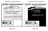
- Figure 3a shows a possible distribution of the potential lines in the structure of the invention functioning as a low side driver, that is, with the source S and the substrate at ground potential and positive voltage applied to the drain D.
- the BODY_BUFFER_REGION should be realized such to become completely depleted because of the inverse biasing of the junction between the body and the DRAIN_WELL before breakdown conditions are reached.
Landscapes
- Insulated Gate Type Field-Effect Transistor (AREA)
Abstract
Description
- The present invention relates to integrated circuits that exploit the so-called RESURF (acronym of REduced SURface Field) condition in which power devices capable of withstanding relatively high voltages, typically n-channel LDMOS and/or lateral p-channel MOS transistors, may respectively function with source or drain untied from ground potential.
- The ability to withstand a relatively high voltage of field effect CMOS lateral transistors such as for example n-channel LDMOS and p-channel MOS transistors may be enhanced through the so-called RESURF technique.
- The RESURF effect is exploited by realizing the integrated circuits in a relatively thin epitaxial layer and by accurately controlling the diffusion implants such to allow integration of lateral CMOS transistors capable to withstand relatively high voltages.
- RESURF LDMOS structures are particularly interesting because they offer an optimal compromise between specific resistance and breakdown voltage, reducing power dissipation as well as the thickness of the silicon dice.
- The main objective to pursue in designing an LDMOS RESURF structure is to ensure that the DRAIN_WELL region be completely depleted before critical electric fields in correspondence with the gate oxide develop.
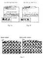
- In order to understand better the principle that characterizes RESURF_LDMOS structures, reference should be made to figures 1a and 1b. The figures show two possible conditions of operation at different drain-source voltages (VDS). The shown LDMOS structure comprises a P-SUBSTRATE, a DRAIN_WELL region having an opposite type of conductivity and a body region. The figures also show the junctions between substrate and DRAIN_WELL and between the DRAIN_WELL and body regions.
- Figure 1a depicts a typical shape of the depletion regions of the two above noted junctions when the source S, the body and the gate G are connected to a reference potential GND and a certain VDS voltage (VDS=20V) is applied to the drain D. Under these conditions of operation, the junctions are inversely biased because of the applied VDS voltage and the respective depletion regions extend into the DRAIN_WELL down to a certain depth.
- By further incrementing the VDS voltage, as shown in Figure 1b (VDS=25V), the depletion regions of the junctions between the substrate and the DRAIN_WELL region and between the DRAIN_WELL region and the body merge, completely depleting the DRAIN_WELL thus producing the desired RESURF condition.
- Under particular conditions of operation, such as in the case of a high side driver, in which relatively high drain gate and source voltages are applied while keeping the substrate to ground potential GND, the total depletion of the DRAIN_WELL may cause precocious punch-through (PT) phenomena between the body and the substrate. For this reason RESURF LDMOS are commonly employed as low side drivers, that is, operated with the source S and the substrate at ground potential.
- There exists a need for a RESURF LDMOS structure capable of functioning a high side driver without the drawbacks and limitations of known devices.
- It has now been found and is the object of the present invention a RESURF LDMOS structure that may be used at relatively high voltages without incurring into unduly precocious punch-through problems.
- The structure of the invention overcomes the problems of the known structures by virtue of an effective anti punch-through (PT) region created between the body and the DRAIN_WELL, having the same type of conductivity of the DRAIN_WELL but being more heavily doped.
- More precisely, the object of the invention is an integrated RESURF LDMOS structure realized in a first region of a first type of conductivity defined in a semiconductor substrate, and comprising a source region of the first type of conductivity formed in a body region of opposite type of conductivity.
- The peculiarity of the invention is that the body region is contained in a portion close to the surface of the semiconductor of the first region more heavily doped that the body region.
- In the most common use of an n-channel RESURF LDMOS structure, and in a process characterized by an n epitaxial layer with thickness of 3 µm, doped with phosphorous at a concentration of 6*1015 atoms cm-3 and where the body region is doped with boron at a concentration of 1018 atoms cm-3, the doping of said superficial portion of the region containing the body region may range between 5*1016 and 1017 atoms cm-3.
- The different aspects and advantages of the invention will become even clearer through the following detailed description and by referring to the details shown in the attached drawings wherein:
- Figures 1a and 1b illustrate the form of the depletion regions in a traditional RESURF LDMOS structure at two different drain-source voltages (VDS);
- Figure 2 shows a traditional LDMOS structure and the LDMOS structure of the invention for pointing out the difference between them;
- Figure 3a shows typical potential lines in the structure of the invention during operation of the LDMOS transistor as a low side driver;
- Figure 3b shows the distribution of the concentrations of charges in the structure of the invention during operation of the LDMOS transistor as a high side driver.
-
- The present invention provides a simple and effective solution to unduly precocious punch-through (PT) problems that normally limit the performance of known RESURF LDMOS structures when functioning as high side drivers, through introducing minor and uncritical changes in the known RESURF LDMOS structure. The invention consists in a RESURF LDMOS structure that includes a superficial portion of the DRAIN_WELL region, surrounding the body region, more heavily doped than the remainder portion of the DRAIN_WELL region, as shown in Figure 2.
- It has now been found that by creating such a superficial BODY_BUFFER_REGION more heavily doped than the bulk of the DRAIN_WELL region, a marked enhancement of the RESURF LDMOS structure performance, especially when functioning as a high side driver at relatively high VDS voltages is achieved. Differently from what occurs in the bulk of the DRAIN_WELL, this superficial region is not completely depleted, thus averting the punch-through problems that restrict the conditions under which present LDMOS structures may safely be employed.
- A better understanding of the principles on which the improved RESURF LDMOS structure of the invention rests may be denied by referring to Figures 3a and 3b.
- As shown in figure 3b, even if relatively high voltages are applied to the drain and source (typical of a high-side functioning), the DRAIN_WELL will be completely depleted of its charges before this condition is reached by the superficial portion of it, herein named BODY_BUFFER_REGION, due to the heavier doping of the latter.
- This effectively prevents the occurrence of punch-through (PT) phenomena at relatively low voltages, practically enhancing the performance of the structure of the invention under critical condition of use.
- In practice, the presence of the BODY_BUFFER_REGION increases the level of voltage that must be reached before punch-through (PT) is caused, while on the other hand it may lower the breakdown voltage (BV).
- The thickness and the doping level of the BODY_BUFFER_REGION should be established for the most appropriate compromise between the requisite of increasing the voltage level at which the punch-through (PT) may occur and the requisite of ensuring a sufficiently high breakdown voltage (BV). These parameters of the BODY_BUFFER_REGION may be accurately established at the design stage such to introduce negligible or tolerable reductions of the breakdown voltage (BV).
- Solely by way of example, the table below give details about likely fabrication process variables. Preferred embodiments of the integrated n-channel RESURF_LDMOS of the invention in a p-type epitaxial layer and of a p-channel RESURF_LDMOS structure in an n-type epitaxial layer may be qualified by the characteristics reported in the following tables, respectively:
region Dopant thickness [µm] doping [atoms cm-3] p-body (conductivity "P") boron 0.25÷0.75 5·1017 ÷5·1018 body-buffer (conductivity "N") phosphorous 0.15÷0.45 5·1016 ÷5·1017 drain well region (conductivity "N") phosphorous 1.5÷4.5 2.5·1015 ÷2.5·1016 region Dopant thickness[µm] doping [atoms cm-3] n-body (conductivity "N") phosphorous 0.25÷0.75 5·1017÷5·1018 body-buffer (conductivity "P") boron 0.15÷0.45 5·1016÷5·1017 drain well region (conductivity "P") boron 1.5÷4.5 2.5·1015÷2.5·1016 - Figure 3a shows a possible distribution of the potential lines in the structure of the invention functioning as a low side driver, that is, with the source S and the substrate at ground potential and positive voltage applied to the drain D.
- The BODY_BUFFER_REGION should be realized such to become completely depleted because of the inverse biasing of the junction between the body and the DRAIN_WELL before breakdown conditions are reached.
- Hence, when the drain voltage assumes values close to those of the expected breakdown voltage, the depletion regions of the inversely biased junctions extend into the BODY_BUFFER_REGION and into the DRAIN_WELL, as shown in figure 3a, thus determining the RESURF condition.
Claims (4)
- A RESURF LDMOS integrated structure realized in a first region (DRAIN_WELL) of a first type of conductivity defined in a semiconductor substrate (P_SUBSTRATE) of opposite type of conductivity and comprising a source region of said first type of conductivity formed in a body region of said opposite type of conductivity, characterized in that
said body region is contained within a superficial portion (BODY_BUFFER_REGION) of said first region (DRAIN_WELL) more heavily doped than the rest of the region. - The integrated structure of claim 1, wherein said first region DRAIN_WELL has a depth comprised between 1.5 and 4.5 micrometers and doping comprised between 2.5*1015 and 2.5*1016 atoms cm-3, said superficial portion (BODY_BUFFER_REGION) is comprised between 0.15 and 0.45 micrometers deep and has a doping comprised between 5*1016 and 5*1017 atoms cm-3 and the depth of said body region is comprised between 0.25 and 0.75 micrometers and has a doping comprised between 5*1017 and 5*1018 atoms cm-3.
- The integrated structure according to claims 1 or 2, wherein said first region (DRAIN_WELL) and said superficial portion thereof (BODY_BUFFER_REGION) are doped with phosphorous while said body region is doped with boron.
- The integrated structure according to one of the claims 1 or 2, wherein said first region (DRAIN_WELL) and said superficial portion thereof (BODY_BUFFER_REGION) are doped with boron while said body region is doped with phosphorus.
Priority Applications (2)
| Application Number | Priority Date | Filing Date | Title |
|---|---|---|---|
| EP00830308A EP1148555A1 (en) | 2000-04-21 | 2000-04-21 | RESURF LDMOS field-effect transistor |
| US09/839,596 US20020011626A1 (en) | 2000-04-21 | 2001-04-20 | RESURF LDMOS integrated structure |
Applications Claiming Priority (1)
| Application Number | Priority Date | Filing Date | Title |
|---|---|---|---|
| EP00830308A EP1148555A1 (en) | 2000-04-21 | 2000-04-21 | RESURF LDMOS field-effect transistor |
Publications (1)
| Publication Number | Publication Date |
|---|---|
| EP1148555A1 true EP1148555A1 (en) | 2001-10-24 |
Family
ID=8175300
Family Applications (1)
| Application Number | Title | Priority Date | Filing Date |
|---|---|---|---|
| EP00830308A Withdrawn EP1148555A1 (en) | 2000-04-21 | 2000-04-21 | RESURF LDMOS field-effect transistor |
Country Status (2)
| Country | Link |
|---|---|
| US (1) | US20020011626A1 (en) |
| EP (1) | EP1148555A1 (en) |
Cited By (1)
| Publication number | Priority date | Publication date | Assignee | Title |
|---|---|---|---|---|
| TWI412134B (en) * | 2005-08-12 | 2013-10-11 | Ciclon Semiconductor Device Corp | Power ldmos transistor |
Families Citing this family (8)
| Publication number | Priority date | Publication date | Assignee | Title |
|---|---|---|---|---|
| US7220633B2 (en) | 2003-11-13 | 2007-05-22 | Volterra Semiconductor Corporation | Method of fabricating a lateral double-diffused MOSFET |
| US7074659B2 (en) * | 2003-11-13 | 2006-07-11 | Volterra Semiconductor Corporation | Method of fabricating a lateral double-diffused MOSFET (LDMOS) transistor |
| US7163856B2 (en) | 2003-11-13 | 2007-01-16 | Volterra Semiconductor Corporation | Method of fabricating a lateral double-diffused mosfet (LDMOS) transistor and a conventional CMOS transistor |
| US7005333B2 (en) | 2003-12-30 | 2006-02-28 | Infineon Technologies Ag | Transistor with silicon and carbon layer in the channel region |
| US7405443B1 (en) | 2005-01-07 | 2008-07-29 | Volterra Semiconductor Corporation | Dual gate lateral double-diffused MOSFET (LDMOS) transistor |
| US7671411B2 (en) * | 2006-03-02 | 2010-03-02 | Volterra Semiconductor Corporation | Lateral double-diffused MOSFET transistor with a lightly doped source |
| US7999318B2 (en) | 2007-12-28 | 2011-08-16 | Volterra Semiconductor Corporation | Heavily doped region in double-diffused source MOSFET (LDMOS) transistor and a method of fabricating the same |
| US20090319423A1 (en) * | 2008-06-24 | 2009-12-24 | Kersenbrock Robert D | Incentive program |
Citations (2)
| Publication number | Priority date | Publication date | Assignee | Title |
|---|---|---|---|---|
| US4975751A (en) * | 1985-09-09 | 1990-12-04 | Harris Corporation | High breakdown active device structure with low series resistance |
| EP0741416A1 (en) * | 1995-05-02 | 1996-11-06 | STMicroelectronics S.r.l. | Thin epitaxy RESURF ic containing HV p-ch and n-ch devices with source or drain not tied to grounds potential |
Family Cites Families (1)
| Publication number | Priority date | Publication date | Assignee | Title |
|---|---|---|---|---|
| US5665988A (en) * | 1995-02-09 | 1997-09-09 | Fuji Electric Co., Ltd. | Conductivity-modulation semiconductor |
-
2000
- 2000-04-21 EP EP00830308A patent/EP1148555A1/en not_active Withdrawn
-
2001
- 2001-04-20 US US09/839,596 patent/US20020011626A1/en not_active Abandoned
Patent Citations (2)
| Publication number | Priority date | Publication date | Assignee | Title |
|---|---|---|---|---|
| US4975751A (en) * | 1985-09-09 | 1990-12-04 | Harris Corporation | High breakdown active device structure with low series resistance |
| EP0741416A1 (en) * | 1995-05-02 | 1996-11-06 | STMicroelectronics S.r.l. | Thin epitaxy RESURF ic containing HV p-ch and n-ch devices with source or drain not tied to grounds potential |
Non-Patent Citations (1)
| Title |
|---|
| BAYER E ET AL: "A 1.0µM LINEAR BICMOS TECHNOLOGY WITH POWER DMOS CAPABILITY", PROCEEDINGS OF THE 1995 BIPOLAR/BICMOS CIRCUITS AND TECHNOLOGY MEETING, MINNEAPOLIS, MN, USA, 2 October 1995 (1995-10-02) - 3 October 1995 (1995-10-03), IEEE, NEW YORK, NY, USA, pages 137 - 141, XP000630211, ISBN: 0-7803-2779-9 * |
Cited By (1)
| Publication number | Priority date | Publication date | Assignee | Title |
|---|---|---|---|---|
| TWI412134B (en) * | 2005-08-12 | 2013-10-11 | Ciclon Semiconductor Device Corp | Power ldmos transistor |
Also Published As
| Publication number | Publication date |
|---|---|
| US20020011626A1 (en) | 2002-01-31 |
Similar Documents
| Publication | Publication Date | Title |
|---|---|---|
| US9871133B2 (en) | Lateral DMOS device with dummy gate | |
| US7238986B2 (en) | Robust DEMOS transistors and method for making the same | |
| US6376315B1 (en) | Method of forming a trench DMOS having reduced threshold voltage | |
| US8847332B2 (en) | Laterally diffused metal oxide semiconductor device having halo or pocket implant region | |
| US11581409B2 (en) | Transistor device with a field electrode that includes two layers | |
| US7315067B2 (en) | Native high-voltage n-channel LDMOSFET in standard logic CMOS | |
| US7238987B2 (en) | Lateral semiconductor device and method for producing the same | |
| US20110198690A1 (en) | Transistor | |
| US7074681B2 (en) | Semiconductor component and method of manufacturing | |
| US5846866A (en) | Drain extension regions in low voltage lateral DMOS devices | |
| US7211845B1 (en) | Multiple doped channel in a multiple doped gate junction field effect transistor | |
| US6664593B2 (en) | Field effect transistor structure and method of manufacture | |
| US20060145285A1 (en) | LDMOS transistor | |
| US6734498B2 (en) | Insulated channel field effect transistor with an electric field terminal region | |
| US7550804B2 (en) | Semiconductor device and method for forming the same | |
| KR20010020486A (en) | Power devices in wide bandgap semiconductor | |
| US20080087949A1 (en) | Semiconductor device and method of manufacturing the same | |
| US20090065863A1 (en) | Lateral double diffused metal oxide semiconductor device | |
| US9887266B2 (en) | Ultra-low drain-source resistance power MOSFET | |
| US20020011626A1 (en) | RESURF LDMOS integrated structure | |
| US9105721B2 (en) | Semiconductor device and manufacturing method thereof | |
| US20070246790A1 (en) | Transistor process using a double-epitaxial layer for reduced capacitance | |
| CN1983633B (en) | High voltage semiconductor component and manufacturing method thereof | |
| JP4248548B2 (en) | High breakdown voltage semiconductor device and manufacturing method thereof | |
| US20070126057A1 (en) | Lateral DMOS device insensitive to oxide corner loss |
Legal Events
| Date | Code | Title | Description |
|---|---|---|---|
| PUAI | Public reference made under article 153(3) epc to a published international application that has entered the european phase |
Free format text: ORIGINAL CODE: 0009012 |
|
| AK | Designated contracting states |
Kind code of ref document: A1 Designated state(s): AT BE CH CY DE DK ES FI FR GB GR IE IT LI LU MC NL PT SE Kind code of ref document: A1 Designated state(s): DE FR GB IT |
|
| AX | Request for extension of the european patent |
Free format text: AL;LT;LV;MK;RO;SI |
|
| 17P | Request for examination filed |
Effective date: 20020402 |
|
| AKX | Designation fees paid |
Free format text: DE FR GB IT |
|
| 17Q | First examination report despatched |
Effective date: 20030812 |
|
| STAA | Information on the status of an ep patent application or granted ep patent |
Free format text: STATUS: THE APPLICATION HAS BEEN WITHDRAWN |
|
| 18W | Application withdrawn |
Effective date: 20080228 |