EP1146634A2 - High frequency oscillation circuit - Google Patents
High frequency oscillation circuit Download PDFInfo
- Publication number
- EP1146634A2 EP1146634A2 EP00127908A EP00127908A EP1146634A2 EP 1146634 A2 EP1146634 A2 EP 1146634A2 EP 00127908 A EP00127908 A EP 00127908A EP 00127908 A EP00127908 A EP 00127908A EP 1146634 A2 EP1146634 A2 EP 1146634A2
- Authority
- EP
- European Patent Office
- Prior art keywords
- frequency
- circuit
- oscillation
- crystal oscillator
- mhz
- Prior art date
- Legal status (The legal status is an assumption and is not a legal conclusion. Google has not performed a legal analysis and makes no representation as to the accuracy of the status listed.)
- Granted
Links
- 230000010355 oscillation Effects 0.000 title claims abstract description 160
- 239000013078 crystal Substances 0.000 claims abstract description 89
- 239000003990 capacitor Substances 0.000 claims description 11
- 238000005259 measurement Methods 0.000 claims description 9
- 239000000126 substance Substances 0.000 claims description 5
- PPBRXRYQALVLMV-UHFFFAOYSA-N Styrene Chemical compound C=CC1=CC=CC=C1 PPBRXRYQALVLMV-UHFFFAOYSA-N 0.000 description 10
- 230000008859 change Effects 0.000 description 8
- 230000004044 response Effects 0.000 description 8
- 239000010408 film Substances 0.000 description 7
- CSCPPACGZOOCGX-UHFFFAOYSA-N Acetone Chemical class CC(C)=O CSCPPACGZOOCGX-UHFFFAOYSA-N 0.000 description 6
- 238000010586 diagram Methods 0.000 description 5
- 238000001179 sorption measurement Methods 0.000 description 5
- 238000000034 method Methods 0.000 description 4
- 238000006116 polymerization reaction Methods 0.000 description 4
- 230000035945 sensitivity Effects 0.000 description 4
- 238000001514 detection method Methods 0.000 description 3
- 230000002349 favourable effect Effects 0.000 description 3
- 230000010485 coping Effects 0.000 description 2
- 239000000428 dust Substances 0.000 description 2
- 239000000463 material Substances 0.000 description 2
- 230000003466 anti-cipated effect Effects 0.000 description 1
- 230000000295 complement effect Effects 0.000 description 1
- 238000007796 conventional method Methods 0.000 description 1
- 230000008878 coupling Effects 0.000 description 1
- 238000010168 coupling process Methods 0.000 description 1
- 238000005859 coupling reaction Methods 0.000 description 1
- 230000000694 effects Effects 0.000 description 1
- 230000002708 enhancing effect Effects 0.000 description 1
- 230000036039 immunity Effects 0.000 description 1
- 230000006872 improvement Effects 0.000 description 1
- 229910044991 metal oxide Inorganic materials 0.000 description 1
- 150000004706 metal oxides Chemical class 0.000 description 1
- 239000000178 monomer Substances 0.000 description 1
- 238000000746 purification Methods 0.000 description 1
- 239000004065 semiconductor Substances 0.000 description 1
- 238000000926 separation method Methods 0.000 description 1
- 230000002459 sustained effect Effects 0.000 description 1
- 239000010409 thin film Substances 0.000 description 1
Images






Classifications
-
- H—ELECTRICITY
- H03—ELECTRONIC CIRCUITRY
- H03B—GENERATION OF OSCILLATIONS, DIRECTLY OR BY FREQUENCY-CHANGING, BY CIRCUITS EMPLOYING ACTIVE ELEMENTS WHICH OPERATE IN A NON-SWITCHING MANNER; GENERATION OF NOISE BY SUCH CIRCUITS
- H03B5/00—Generation of oscillations using amplifier with regenerative feedback from output to input
- H03B5/30—Generation of oscillations using amplifier with regenerative feedback from output to input with frequency-determining element being electromechanical resonator
- H03B5/32—Generation of oscillations using amplifier with regenerative feedback from output to input with frequency-determining element being electromechanical resonator being a piezoelectric resonator
- H03B5/36—Generation of oscillations using amplifier with regenerative feedback from output to input with frequency-determining element being electromechanical resonator being a piezoelectric resonator active element in amplifier being semiconductor device
Definitions
- the present invention relates to a high-frequency oscillation circuit, and more particularly, to a high-frequency oscillation circuit useful for enhancing sensitivity of various measuring instruments used as weight sensor, chemical sensor, biosensor, viscosity sensor, film thickness meter, gas sensor, floating dust sensor, immunity sensor or the like.
- a wafer used for a crystal oscillator has such a nature as to cause distortion (piezo-electric effect) when a voltage is applied to thin film electrodes attached to both side faces faces thereof and return to its initial state when the voltage is removed. Because of this nature, a crystal oscillator oscillates at a natural frequency determined by its thickness. Thereby, in a crystal wafer, when its thickness varies by adsorbing a substance, a basic frequency (i.e., the natural oscillation frequency or basic oscillation frequency) of the crystal oscillator is varied.
- ⁇ f - ⁇ 2f 0 2 /( ⁇ q x ⁇ q) 1/2 ⁇ ⁇ ( ⁇ m/A)
- f 0 is a basic oscillation frequency
- ⁇ q and ⁇ q are density and elastic modulus of the crystal, respectively
- A is the area of a portion performing piezo-electric response.
- JP-A-3-165236 JP-A means unexamined published Japanese patent application
- JP-A means unexamined published Japanese patent application
- the Electronic Circuit Parts Utilization Handbook p.67, by CQ Publishing Co., issued on November 1, 1985.
- This oscillation circuits use only an oscillator having a natural frequency in a low-frequency area, so that it cannot cope with a demand for higher sensitivity, making it hard to realize a high-frequency oscillation circuit showing high-frequency stability.
- the present invention overturns common knowledge of a conventional oscillation circuit.
- the present invention aims to provide a high-frequency oscillation circuit which can keep a stable high-frequency oscillation to easily cope with the natural oscillation frequency of a crystal oscillator as a sensor even if it becomes high, and yet which can be easily manufactured at a low cost.
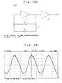
- Fig. 1(a) is a diagram showing an embodiment of a high-frequency oscillation circuit using a logic element "NAND” and a crystal oscillator having a basic oscillation frequency of 50 MHz.
- Fig. 1(b) is a graph showing an oscillation waveform of the circuit in Fig. 1(a).
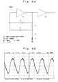
- Fig. 2(a) is a diagram showing an embodiment of a high-frequency oscillation circuit using a logic element "NAND” and a crystal oscillator having a basic oscillation frequency of 100 MHz.
- Fig. 2(b) is a graph showing an oscillation waveform of the circuit in Fig. 2(a).
- Fig. 3(a) is a diagram showing an embodiment of a high-frequency oscillation circuit using a logic element "inverter” and a crystal oscillator having a basic oscillation frequency of 155 MHz.
- Fig. 3(b) is a graph showing an oscillation waveform of the circuit in Fig. 3(a).
- Fig. 4(a) is a diagram showing an embodiment of a high-frequency oscillation circuit using a logic element "inverter” and an overtone crystal oscillator of 100 MHz.
- Fig. 4(b) is a graph showing an oscillation waveform of the circuit in Fig. 4(a).
- Fig. 5 is a graph showing the stability of an oscillation frequency per hour of the circuit shown in Fig. 2(a) in case of using a normal crystal oscillator.
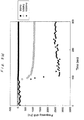
- Fig. 6 is a graph showing the stability of an oscillation frequency per hour of the circuit shown in Fig. 2(a) in case of using a crystal oscillator on which a styrene film was deposited for one minute by the plasma polymerization method.
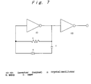
- Fig. 7 is a diagram showing another embodiment of the high-frequency oscillation circuit of the present invention.
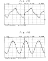
- Fig. 8(a) is a graph showing an oscillation waveform measured by oscilloscope in case a crystal oscillator having a basic oscillation frequency of 20 MHz is used in the circuit shown in Fig. 7.
- Fig. 8(b) is a graph showing an oscillation waveform measured by oscilloscope in case a crystal oscillator having a basic oscillation frequency of 33 MHz is used in the circuit shown in Fig. 7.
- Fig. 8(c) is a graph showing an oscillation waveform measured by oscilloscope in case a crystal oscillator with a basic oscillation frequency of 50 MHz is used in the circuit shown in Fig. 7.
- Fig. 8(d) is a graph showing an oscillation waveform measured by oscilloscope in case a crystal oscillator having a basic oscillation frequency of 155 MHz is used in the circuit shown in Fig. 7.
- Fig. 9(a) is a graph showing changes in the oscillation frequency with the lapse of time when one of the oscillation circuits of Fig. 7 is used and saturated acetone steam of the same concentration is adsorbed on crystal oscillators coated with a plasma polymerized styrene film of the same weight .
- Fig. 9(b) is an enlarged graph of the measurement result by using the crystal oscillator having the basic oscillation frequency of 9 MHz in Fig. 9(a).
- the inventor used a readily available logic element, made a closed circuit by connecting its input and output with a capacitor, a resistor and a crystal oscillator having a natural oscillation frequency in a high-frequency area, and discovered that an oscillation circuit capable of keeping a more stable high-frequency oscillation can be unexpectedly obtained by the operation time or response speed of the logic element, the time constant of the capacitor and the resistor or the like, resulting in completion of the present invention.
- the present invention provides a high-frequency oscillation circuit characterized by incorporating a crystal oscillator having a natural oscillation frequency (i.e., basic oscillation frequency) in a high-frequency area into a closed circuit including a logic element.
- a natural oscillation frequency i.e., basic oscillation frequency
- a closed circuit is formed by using a logic element.
- a logic element such as NAND circuit, NOR circuit, inverter or the like which is heretofore publicly known, but it is preferable to use a high-speed TTL (Transistor-Transistor Logic) element or CMOS (Complementary Metal Oxide Semiconductor) element so as to cope with a high-frequency oscillation.
- TTL Transistor-Transistor Logic
- CMOS Complementary Metal Oxide Semiconductor
- a crystal oscillator having a natural oscillation frequency in a high-frequency area a crystal oscillator having a natural oscillation frequency corresponding to the oscillation frequency of the circuit generally between 30 and 1800 MHz, preferably between 50 and 1800 MHz, more preferably between 100 and 1800 MHz, and the most preferably between 150 and 1800 MHz can be given.
- a crystal oscillator for high frequency a crystal oscillator having a basic oscillation frequency corresponding to an oscillation frequency generally between 1 MHz and 2GHz, preferably of 150 MHz or more can be given as an example.
- the high-frequency oscillation circuit in the high-frequency oscillation circuit relative to the present invention, it is possible to incorporate a crystal oscillator having a basic oscillation frequency in a high-frequency area into a closed circuit including a high-frequency CMOS as a logic element.
- This oscillation circuit has quite a novel circuit content and circuit constitution of a type that could not be anticipated or expected by the conventional electronic circuit.
- Such a high-frequency oscillation circuit as this is suited for oscillation of an oscillator, particularly a crystal oscillator for chemical measurement.
- the closed circuit in the present invention can be formed by connecting a capacitor, a resistor and a crystal oscillator having a natural oscillation frequency in a high-frequency area to the input and output of such a logic element, and properly adjusting an operation time or response speed of the logic element, the natural oscillation frequency of the crystal oscillator, and the time constant or the like of the capacitor and resistor.
- an embodiment to select a high-speed TTL or CMOS to suit the natural oscillation frequency in a high-frequency area of the crystal oscillator incorporated into the closed circuit, or an embodiment to select a logic element CMOS having a response speed capable of coping with the basic oscillation frequency in the high-frequency area is preferable.
- Figs. 1 and 2 The high-frequency oscillation circuits, in case a logic element NAND is used, are shown in Figs. 1 and 2, respectively.
- Fig. 1(a) shows an example of an oscillation circuit when a crystal oscillator X1 for a basic frequency of 50 MHz is used;
- Fig. 1(b) shows an oscillation waveform of the same circuit as measured by using an oscilloscope.
- Fig. 2(a) shows an example of an oscillation circuit when an overtone (oscillation frequency of a sub-oscillation) crystal oscillator X2 in the 3rd or 5th order of 100 MHz is used;
- Fig. 2(b) shows an oscillation waveform of the same circuit as measured by using an oscilloscope.
- IC1 - IC3 are NANDs as logic elements
- X1 is a crystal oscillator having a basic oscillation frequency of 50 MHz
- X2 is a crystal oscillator having a basic oscillation frequency of 100 MHz
- C1 - C3 are capacitors
- R1 - R2 are resistors.
- Each closed circuit is constituted by connecting the output of the logic element IC1 to the input of IC2, and connecting the output of IC2 to the input of IC1.
- IC3 is a buffer for taking out the output of the oscillation circuit to the outside.
- a crystal oscillator X1 or X2 is disposed in each of closed circuits. The impedance of each of the crystal oscillators X1 and X2 becomes the lowest at their natural oscillation frequencies (i.e., basic oscillation frequencies).
- each capacitor C and each resistor R are set at such a value as the circuit impedance has the lowest value where the impedance of the crystal oscillators X1 or X2 is the lowest, in view of the operating speed of the logic element IC.
- Fig. 1(a) and Fig. 2(a) The values of the above circuit components (parts) and the names of the logic elements are shown in Fig. 1(a) and Fig. 2(a), respectively.
- Fig. 1(a) the type of the logic elements IC1, IC2 and IC3 are 74LS00; C1 is 10pF; C2 is 7pF; C3 is 100pF; R1 is 470 ⁇ ; and R2 is 330 ⁇ .
- Fig. 2(a) the type of the logic elements IC1, IC2 and IC3 are 74HC00; C2 is 1pF; C3 is 100pF; R1 and R2 are 300 ⁇ .
- Figs. 3 and 4 show oscillation circuits, in case an inverter is used as a logic element, respectively.
- Fig. 3 shows an example of using a crystal oscillator X1 having a basic oscillation frequency of 155 MHz.
- Fig. 4 shows an example of using an overtone crystal oscillator X2 in the 3rd or 5th of 100 MHz.
- the logic element IC is an inverter and L1 is an inductance. Also, IC2 is a buffer to take out the output of the oscillation circuit outside.
- a closed circuit is constituted by connecting the input and output of the inverter IC1.
- the crystal oscillator X1 or X2 is disposed in this closed circuit. The impedance of each of the crystal oscillators X1 and X2 becomes the lowest at their natural oscillation frequencies. Consequently, each oscillation circuit oscillates at the natural oscillation frequency of the crystal oscillator X1 or X2.
- Fig. 3(a) shows an example of a circuit which excites the optimum oscillation at the basic oscillation frequency of the crystal oscillator X1.
- the basic oscillation frequency of the crystal oscillator X1 in this example is 155 MHz.
- the values of the capacitor C1 and the resistor R1 which are concrete circuit parts as well as the name of the logic element IC are shown in the drawing.
- Fig. 4(a) shows an example of a circuit which oscillates the most favorably at each overtone.
- C1 and L1 are for selecting a desired order.
- the drawings show the value of the circuit parts and the name of the logic element in case the circuit is oscillated at the natural oscillation frequency of 100 MHz by using the 5th order (or 3rd order of 33 MHz) of the crystal oscillator X2 having the basic oscillation frequency of 20 MHz.
- the type of the logic elements IC1 and IC2 are 74HCU04AP; C1 is 50pF; R1 is 500k ⁇ ; and L1 is 0.5 ⁇ H.
- the type of the logic elements IC1 and IC2 are 74HCU04; C1 is 150pF; R1 is 100 ⁇ ; and L1 is 0.5 ⁇ H.
- circuit parts and name of logic element are not definite, but it is the same as in case of Embodiments 1 in that, if a value is in the vicinity, the impedance of the circuit is low enough, so the circuit will oscillate at the natural oscillation frequency of the crystal oscillator X1 or X2.
- the waveforms at the above circuit constant show a substantially pure sine wave, and the frequency can be measured accurately enough by an ordinary frequency counter.
- Fig. 5 shows the degree of stability of the oscillation frequency in an hour in case of the circuit having the oscillation frequency of 100 MHz using an ordinary crystal oscillator, in the Embodiment shown in Fig. 2(a).
- Fig. 6 shows the degree of stability of the oscillation frequency in an hour in case of the circuit using a crystal oscillator on which a styrene film is deposited for one minute by a plasma-polymerization method, in which the circuit having an oscillation frequency of 100 MHz is the same one of the embodiment as shown in Fig. 2(a).
- the variation in oscillation frequency of the circuit per hour is of a value within the range of 10 Hz.
- the variation in oscillation frequency per hour of the circuit using the crystal oscillator on which a styrene film is deposited for one minute by plasma polymerization method is also within the range of 10 Hz.
- each of the circuits in Embodiments 2 shows the same oscillation property of a highly stable high-frequency as in Embodiments 1.
- FIG. 7 shows an oscillation circuit using a crystal oscillator whose basic oscillation frequency is between 20 MHz and 155 MHz.
- IC1 and IC2 are inverters as logic elements; X is a crystal oscillator; C is a capacitor; and R is a resistor. The concrete values of the capacitor C and the resistor R and the name of the logic element IC are shown in the drawing. Further, IC2 is a buffer to take out the output of the oscillation circuit outside.
- a closed circuit is constituted by connecting the input and the output of the inverter IC1.
- the crystal oscillator X is placed in this closed circuit.
- the impedance of the crystal oscillator X becomes the lowest at its basic oscillation frequency. Accordingly, the circuit will oscillate at the natural oscillation frequency of the crystal oscillator X.
- the oscillation frequency can be 1 to 19 MHz, 20 MHz, 33 MHz, 50 MHz, and 155 MHz in the circuit of Fig. 7.
- the type of the inverter IC1 and IC2 is 74HCU04AP; R is 500 k ⁇ ; and C is 1000 pF.
- the above values of the circuit elements and the names of the logic elements are not restrictive, but, since the impedance of the circuit is low enough in the vicinities, the oscillation circuit oscillates at the basic oscillation frequency of the crystal oscillator X. It is desirable to select a logic element CMOS capable of coping with this range of frequency.
- Fig 8(a), (b), (c) and (d) show output waveforms measured by an oscilloscope in case crystal oscillators X having basic oscillation frequencies of 20 MHz, 33 MHz, 50 MHz, and 155 MHz are respectively used in the circuit of Fig. 7.
- the output waveform by the above circuit constant has a shape between a rectangular and a sine wave and shows approximately a sine wave at 155 MHz.
- the oscillation frequency of the oscillation circuit showing these output waveforms can be sufficiently measured by an ordinary frequency counter.
- crystal oscillators X having various basic oscillation frequencies from 1 MHz to 2 GHz, they can be oscillated on the same circuit at the basic oscillation frequency of each crystal oscillator.
- crystal oscillators X having various basic oscillation frequencies from 1 MHz to 2 GHz, they can be oscillated on the same circuit at the basic oscillation frequency of each crystal oscillator.
- it has been a common knowledge to design and constitute an oscillation circuit the most favorable for each crystal oscillator.
- the present invention overturns the common knowledge regarding conventional oscillation circuits.
- Figs. 9(a) and 9(b) show changes in the oscillation frequency with the lapse of time when one of the oscillation circuits of Fig. 7 is used and saturated acetone steam of the same concentration (as measured by extracting 2 ml of head space of the acetone solution and injecting it into a gas adsorption measurement vessel of 1000 ml) is adsorbed on crystal oscillators (of 9 MHz, 50 MHz, 155 MHz) coated with a plasma polymerized styrene film of the same weight (subjected to electric discharge output of 100 W, monomer pressure of 100 Pa, and 1 minute of polymerization time).
- gas adsorption responses are shown, when measured, respectively, by using: ( ⁇ ) a crystal oscillator having a basic oscillation frequency of 9 MHz; ( ⁇ ) a crystal oscillator having a basic oscillation frequency of 50 MHz; and ( ⁇ ) a crystal oscillator having a basic oscillation frequency of 155 MHz.
- the basic oscillation frequencies of the crystal increase, the amount of change in frequency responding to the acetone steam of the same concentration remarkably increases.
- the high-frequency oscillation circuit using the logic elements according to the present invention continues highly stable oscillation by a crystal oscillator having a high natural oscillation frequency.
- the high-frequency oscillation circuit of the present invention enables to measure precisely a delicate change in natural oscillation frequency of a crystal oscillator as a sensor, and a use of such a high-frequency oscillation circuit enables to readily fabricate a super-high-sensitive, precision measurement instrument favorable for measurement such as a super-high sensitive weight sensor, a viscosity sensor, and the like.
Landscapes
- Oscillators With Electromechanical Resonators (AREA)
Abstract
Description
Claims (10)
- A high-frequency oscillation circuit comprising a closed circuit including one or more logic elements, and a crystal oscillator for high frequency disposed within said closed circuit.
- A high-frequency oscillation circuit as claimed in claim 1, further comprising a capacitor and a resistor disposed within said closed circuit.
- A high-frequency oscillation circuit as claimed in claim 1, further comprising a resistor disposed within said closed circuit, and a capacitor disposed outside said closed circuit and connected with said closed circuit.
- A high-frequency oscillation circuit as claimed in one of claims 1 through 3, wherein said logic element includes a high-speed TTL or CMOS.
- A high-frequency oscillation circuit as claimed in one of claims 1 through 4, wherein a crystal oscillator of high frequency of 30 MHz or more is used as said crystal oscillator.
- A high-frequency oscillation circuit as claimed in one of claims 1 through 3, wherein said closed circuit is formed by disposing one logic element and wherein said crystal oscillator has a basic oscillation frequency in a high frequency area.
- A high-frequency oscillation circuit as claimed in claim 6, wherein said logic element includes a high-speed CMOS.
- A high-frequency oscillation circuit as claimed in claim 6 or 7, which is oscillated by a crystal oscillator having a basic oscillation frequency in an oscillation frequency area of 1 MHz to 500 MHz or more than 500 MHz with the same circuit constitution.
- A high-frequency oscillation circuit as claimed in one of claims 6 through 8, wherein said crystal oscillator is used as a sensor element for chemical measurement.
- A high-frequency oscillation circuit as claimed in one of claims 1 through 9, wherein said closed circuit is formed so as to connect the input and output of said logic elements.
Applications Claiming Priority (4)
| Application Number | Priority Date | Filing Date | Title |
|---|---|---|---|
| JP2000031513A JP2001221732A (en) | 2000-02-09 | 2000-02-09 | High frequency oscillation circuit showing high frequency stability |
| JP2000031513 | 2000-02-09 | ||
| JP2000103709 | 2000-04-05 | ||
| JP2000103709A JP2001289765A (en) | 2000-04-05 | 2000-04-05 | High-frequency oscillation circuit that drives a crystal oscillator for chemical measurement |
Publications (4)
| Publication Number | Publication Date |
|---|---|
| EP1146634A2 true EP1146634A2 (en) | 2001-10-17 |
| EP1146634A3 EP1146634A3 (en) | 2002-02-06 |
| EP1146634B1 EP1146634B1 (en) | 2010-03-17 |
| EP1146634B8 EP1146634B8 (en) | 2010-05-26 |
Family
ID=26585087
Family Applications (1)
| Application Number | Title | Priority Date | Filing Date |
|---|---|---|---|
| EP00127908A Expired - Lifetime EP1146634B8 (en) | 2000-02-09 | 2000-12-20 | High frequency oscillation circuit |
Country Status (6)
| Country | Link |
|---|---|
| US (1) | US6798306B2 (en) |
| EP (1) | EP1146634B8 (en) |
| AU (1) | AU767454B2 (en) |
| CA (1) | CA2328813C (en) |
| DE (1) | DE60044021D1 (en) |
| NZ (1) | NZ508983A (en) |
Families Citing this family (3)
| Publication number | Priority date | Publication date | Assignee | Title |
|---|---|---|---|---|
| JP2004023109A (en) * | 2002-06-12 | 2004-01-22 | Seiko Epson Corp | Oscillation circuit and semiconductor integrated circuit |
| EP2779456B1 (en) * | 2013-03-15 | 2018-08-29 | Dialog Semiconductor B.V. | Method for reducing overdrive need in mos switching and logic circuit |
| DE102020001370A1 (en) * | 2020-02-25 | 2021-08-26 | Hilti Aktiengesellschaft | Method and device for the capacitive measurement of substance concentrations |
Family Cites Families (12)
| Publication number | Priority date | Publication date | Assignee | Title |
|---|---|---|---|---|
| US3879992A (en) | 1970-05-12 | 1975-04-29 | California Inst Of Techn | Multiple crystal oscillator measuring apparatus |
| US3689907A (en) * | 1970-08-03 | 1972-09-05 | Robbins Aviat Inc | Dewpoint monitor |
| US3676801A (en) * | 1970-10-28 | 1972-07-11 | Motorola Inc | Stabilized complementary micro-power square wave oscillator |
| US3760290A (en) | 1972-06-16 | 1973-09-18 | Quinder Electronics Inc | Crystal controlled variable frequency oscillator |
| US4321562A (en) * | 1979-01-11 | 1982-03-23 | Nippon Electric Co., Ltd. | Crystal oscillator circuit capable of changing the number of inverter stages coupled in series |
| CA1227357A (en) * | 1985-02-12 | 1987-09-29 | Minister Of National Defence | Method and apparatus for detecting presence and concentration of vapours in gaseous fluids |
| US4862114A (en) * | 1988-06-23 | 1989-08-29 | The United States Of America As Represented By The Administrator Of The National Aeronautics And Space Administration | Crystal oscillators using negative voltage gain, single pole response amplifiers |
| JPH0752592B2 (en) | 1989-08-18 | 1995-06-05 | 株式会社東芝 | Semiconductor memory device |
| JPH03165236A (en) | 1989-11-24 | 1991-07-17 | Seiko Instr Inc | Oscillating circuit for piezoelectric element |
| JPH05273106A (en) | 1992-03-24 | 1993-10-22 | Toshiba Corp | Sulfur hexafluoride decomposed gas sensor |
| JPH07131249A (en) | 1993-10-29 | 1995-05-19 | Meidensha Corp | Crystal oscillation circuit |
| WO1996003799A1 (en) * | 1994-07-27 | 1996-02-08 | Citizen Watch Co., Ltd. | Temperature compensation type quartz oscillator |
-
2000
- 2000-12-18 CA CA002328813A patent/CA2328813C/en not_active Expired - Fee Related
- 2000-12-19 NZ NZ508983A patent/NZ508983A/en unknown
- 2000-12-19 AU AU72381/00A patent/AU767454B2/en not_active Ceased
- 2000-12-20 DE DE60044021T patent/DE60044021D1/en not_active Expired - Lifetime
- 2000-12-20 EP EP00127908A patent/EP1146634B8/en not_active Expired - Lifetime
- 2000-12-20 US US09/739,812 patent/US6798306B2/en not_active Expired - Fee Related
Also Published As
| Publication number | Publication date |
|---|---|
| AU767454B2 (en) | 2003-11-13 |
| EP1146634B8 (en) | 2010-05-26 |
| AU7238100A (en) | 2001-08-16 |
| CA2328813C (en) | 2005-09-20 |
| EP1146634B1 (en) | 2010-03-17 |
| US20020075089A1 (en) | 2002-06-20 |
| DE60044021D1 (en) | 2010-04-29 |
| NZ508983A (en) | 2002-10-25 |
| CA2328813A1 (en) | 2001-08-09 |
| US6798306B2 (en) | 2004-09-28 |
| EP1146634A3 (en) | 2002-02-06 |
Similar Documents
| Publication | Publication Date | Title |
|---|---|---|
| US8434350B2 (en) | Apparatus for determining and/or monitoring a process variable of a medium | |
| RU2271603C2 (en) | Time standard built around adjustable integrated micromechanical tuning-fork resonator | |
| US4507970A (en) | Pressure sensitive element and a sensor comprising such an element | |
| US4734609A (en) | Gas density transducer | |
| KR102799340B1 (en) | FBAR Oscillator and Gas Sensing System using the FBAR Oscillator | |
| US7378781B2 (en) | Acoustic wave resonator with integrated temperature control for oscillator purposes | |
| JP5013250B2 (en) | Acceleration sensor | |
| Kaajakari et al. | A 32.768 kHz MEMS resonator with+/-20 ppm tolerance in 0.9 mm x 0.6 mm chip scale package | |
| JP2009100480A (en) | Quartz crystal unit and method of manufacturing quartz crystal oscillator | |
| JPH08278336A (en) | Electrostatic sensor device | |
| EP1146634B1 (en) | High frequency oscillation circuit | |
| JPH10142134A (en) | Odor measurement device | |
| JP5040798B2 (en) | Piezoelectric oscillator | |
| RU2352907C2 (en) | Device for determination and/or control of medium process parameter | |
| EP1679506A2 (en) | SC cut crystal microbalance | |
| JP4773656B2 (en) | Frequency warping to improve the S / N ratio of the resonator | |
| CN116436408A (en) | Square wave generating circuit | |
| KR100500356B1 (en) | Piezoelectric resonator and fm detection circuit incorporating the same | |
| JP2004328701A (en) | Manufacturing method of crystal oscillator | |
| JP2001289765A (en) | High-frequency oscillation circuit that drives a crystal oscillator for chemical measurement | |
| JP3849014B2 (en) | High frequency oscillation circuit | |
| JP2009272734A (en) | Piezoelectric oscillator | |
| JP2686991B2 (en) | Overtone oscillator circuit | |
| Zakrzewski | Error propagation in the Interface Electronics for passive sensors | |
| KR100210334B1 (en) | Vibration gyroscope and method for adjusting vibration-gyroscope characteristics |
Legal Events
| Date | Code | Title | Description |
|---|---|---|---|
| PUAI | Public reference made under article 153(3) epc to a published international application that has entered the european phase |
Free format text: ORIGINAL CODE: 0009012 |
|
| 17P | Request for examination filed |
Effective date: 20001220 |
|
| AK | Designated contracting states |
Kind code of ref document: A2 Designated state(s): CH DE FR GB LI SE Kind code of ref document: A2 Designated state(s): AT BE CH CY DE DK ES FI FR GB GR IE IT LI LU MC NL PT SE TR |
|
| AX | Request for extension of the european patent |
Free format text: AL;LT;LV;MK;RO;SI |
|
| PUAL | Search report despatched |
Free format text: ORIGINAL CODE: 0009013 |
|
| AK | Designated contracting states |
Kind code of ref document: A3 Designated state(s): AT BE CH CY DE DK ES FI FR GB GR IE IT LI LU MC NL PT SE TR |
|
| AX | Request for extension of the european patent |
Free format text: AL;LT;LV;MK;RO;SI |
|
| 17Q | First examination report despatched |
Effective date: 20020612 |
|
| AKX | Designation fees paid |
Free format text: CH DE FR GB LI SE |
|
| GRAP | Despatch of communication of intention to grant a patent |
Free format text: ORIGINAL CODE: EPIDOSNIGR1 |
|
| GRAS | Grant fee paid |
Free format text: ORIGINAL CODE: EPIDOSNIGR3 |
|
| GRAA | (expected) grant |
Free format text: ORIGINAL CODE: 0009210 |
|
| AK | Designated contracting states |
Kind code of ref document: B1 Designated state(s): CH DE FR GB LI SE |
|
| REG | Reference to a national code |
Ref country code: GB Ref legal event code: FG4D |
|
| REG | Reference to a national code |
Ref country code: CH Ref legal event code: EP |
|
| REF | Corresponds to: |
Ref document number: 60044021 Country of ref document: DE Date of ref document: 20100429 Kind code of ref document: P |
|
| RAP2 | Party data changed (patent owner data changed or rights of a patent transferred) |
Owner name: NATIONAL INSTITUTE OF ADVANCED INDUSTRIAL SCIENCE |
|
| PG25 | Lapsed in a contracting state [announced via postgrant information from national office to epo] |
Ref country code: SE Free format text: LAPSE BECAUSE OF FAILURE TO SUBMIT A TRANSLATION OF THE DESCRIPTION OR TO PAY THE FEE WITHIN THE PRESCRIBED TIME-LIMIT Effective date: 20100317 |
|
| PLBE | No opposition filed within time limit |
Free format text: ORIGINAL CODE: 0009261 |
|
| STAA | Information on the status of an ep patent application or granted ep patent |
Free format text: STATUS: NO OPPOSITION FILED WITHIN TIME LIMIT |
|
| 26N | No opposition filed |
Effective date: 20101220 |
|
| REG | Reference to a national code |
Ref country code: CH Ref legal event code: PL |
|
| REG | Reference to a national code |
Ref country code: FR Ref legal event code: ST Effective date: 20110831 |
|
| PG25 | Lapsed in a contracting state [announced via postgrant information from national office to epo] |
Ref country code: CH Free format text: LAPSE BECAUSE OF NON-PAYMENT OF DUE FEES Effective date: 20101231 Ref country code: LI Free format text: LAPSE BECAUSE OF NON-PAYMENT OF DUE FEES Effective date: 20101231 Ref country code: FR Free format text: LAPSE BECAUSE OF NON-PAYMENT OF DUE FEES Effective date: 20110103 |
|
| REG | Reference to a national code |
Ref country code: DE Ref legal event code: R119 Ref document number: 60044021 Country of ref document: DE Effective date: 20110701 |
|
| PG25 | Lapsed in a contracting state [announced via postgrant information from national office to epo] |
Ref country code: DE Free format text: LAPSE BECAUSE OF NON-PAYMENT OF DUE FEES Effective date: 20110701 |
|
| PGFP | Annual fee paid to national office [announced via postgrant information from national office to epo] |
Ref country code: GB Payment date: 20121220 Year of fee payment: 13 |
|
| GBPC | Gb: european patent ceased through non-payment of renewal fee |
Effective date: 20131220 |
|
| PG25 | Lapsed in a contracting state [announced via postgrant information from national office to epo] |
Ref country code: GB Free format text: LAPSE BECAUSE OF NON-PAYMENT OF DUE FEES Effective date: 20131220 |