EP1146613A1 - Semiconductor laser module and method of driving semiconductor laser module - Google Patents
Semiconductor laser module and method of driving semiconductor laser module Download PDFInfo
- Publication number
- EP1146613A1 EP1146613A1 EP00927782A EP00927782A EP1146613A1 EP 1146613 A1 EP1146613 A1 EP 1146613A1 EP 00927782 A EP00927782 A EP 00927782A EP 00927782 A EP00927782 A EP 00927782A EP 1146613 A1 EP1146613 A1 EP 1146613A1
- Authority
- EP
- European Patent Office
- Prior art keywords
- thermomodule
- semiconductor laser
- optical fiber
- laser element
- substrate
- Prior art date
- Legal status (The legal status is an assumption and is not a legal conclusion. Google has not performed a legal analysis and makes no representation as to the accuracy of the status listed.)
- Granted
Links
- 239000004065 semiconductor Substances 0.000 title claims abstract description 175
- 238000000034 method Methods 0.000 title claims description 14
- 238000010438 heat treatment Methods 0.000 claims abstract description 71
- 230000009471 action Effects 0.000 claims abstract description 32
- 238000001816 cooling Methods 0.000 claims abstract description 19
- 239000013307 optical fiber Substances 0.000 claims description 79
- 239000000758 substrate Substances 0.000 claims description 53
- 230000004044 response Effects 0.000 claims description 9
- 230000005540 biological transmission Effects 0.000 claims description 8
- 239000000463 material Substances 0.000 claims description 5
- 238000011144 upstream manufacturing Methods 0.000 claims description 5
- 239000004020 conductor Substances 0.000 claims description 4
- 238000002844 melting Methods 0.000 claims description 4
- 230000008018 melting Effects 0.000 claims description 4
- 230000002265 prevention Effects 0.000 claims description 4
- 230000003287 optical effect Effects 0.000 description 18
- 238000010276 construction Methods 0.000 description 12
- 229910000679 solder Inorganic materials 0.000 description 12
- 239000003990 capacitor Substances 0.000 description 11
- 230000008878 coupling Effects 0.000 description 8
- 238000010168 coupling process Methods 0.000 description 8
- 238000005859 coupling reaction Methods 0.000 description 8
- 238000010521 absorption reaction Methods 0.000 description 3
- 230000000694 effects Effects 0.000 description 3
- 238000003780 insertion Methods 0.000 description 3
- 230000037431 insertion Effects 0.000 description 3
- 229910052751 metal Inorganic materials 0.000 description 3
- 239000002184 metal Substances 0.000 description 3
- 239000013078 crystal Substances 0.000 description 2
- 230000007547 defect Effects 0.000 description 2
- 230000006866 deterioration Effects 0.000 description 2
- 230000002542 deteriorative effect Effects 0.000 description 2
- 230000005496 eutectics Effects 0.000 description 2
- 238000005086 pumping Methods 0.000 description 2
- 238000005476 soldering Methods 0.000 description 2
- 229910017709 Ni Co Inorganic materials 0.000 description 1
- 229910003267 Ni-Co Inorganic materials 0.000 description 1
- 229910003262 Ni‐Co Inorganic materials 0.000 description 1
- 229910020658 PbSn Inorganic materials 0.000 description 1
- 101150071746 Pbsn gene Proteins 0.000 description 1
- VYPSYNLAJGMNEJ-UHFFFAOYSA-N Silicium dioxide Chemical compound O=[Si]=O VYPSYNLAJGMNEJ-UHFFFAOYSA-N 0.000 description 1
- 230000002159 abnormal effect Effects 0.000 description 1
- 229910045601 alloy Inorganic materials 0.000 description 1
- 239000000956 alloy Substances 0.000 description 1
- PNEYBMLMFCGWSK-UHFFFAOYSA-N aluminium oxide Inorganic materials [O-2].[O-2].[O-2].[Al+3].[Al+3] PNEYBMLMFCGWSK-UHFFFAOYSA-N 0.000 description 1
- PMHQVHHXPFUNSP-UHFFFAOYSA-M copper(1+);methylsulfanylmethane;bromide Chemical compound Br[Cu].CSC PMHQVHHXPFUNSP-UHFFFAOYSA-M 0.000 description 1
- 238000010586 diagram Methods 0.000 description 1
- 230000002349 favourable effect Effects 0.000 description 1
- 230000004927 fusion Effects 0.000 description 1
- 239000011521 glass Substances 0.000 description 1
- 238000009413 insulation Methods 0.000 description 1
- 238000012986 modification Methods 0.000 description 1
- 230000004048 modification Effects 0.000 description 1
- 230000005855 radiation Effects 0.000 description 1
- 239000010935 stainless steel Substances 0.000 description 1
- 229910001220 stainless steel Inorganic materials 0.000 description 1
- 238000003466 welding Methods 0.000 description 1
Images


Classifications
-
- H—ELECTRICITY
- H01—ELECTRIC ELEMENTS
- H01S—DEVICES USING THE PROCESS OF LIGHT AMPLIFICATION BY STIMULATED EMISSION OF RADIATION [LASER] TO AMPLIFY OR GENERATE LIGHT; DEVICES USING STIMULATED EMISSION OF ELECTROMAGNETIC RADIATION IN WAVE RANGES OTHER THAN OPTICAL
- H01S5/00—Semiconductor lasers
- H01S5/02—Structural details or components not essential to laser action
- H01S5/024—Arrangements for thermal management
- H01S5/02407—Active cooling, e.g. the laser temperature is controlled by a thermo-electric cooler or water cooling
- H01S5/02415—Active cooling, e.g. the laser temperature is controlled by a thermo-electric cooler or water cooling by using a thermo-electric cooler [TEC], e.g. Peltier element
-
- H—ELECTRICITY
- H01—ELECTRIC ELEMENTS
- H01S—DEVICES USING THE PROCESS OF LIGHT AMPLIFICATION BY STIMULATED EMISSION OF RADIATION [LASER] TO AMPLIFY OR GENERATE LIGHT; DEVICES USING STIMULATED EMISSION OF ELECTROMAGNETIC RADIATION IN WAVE RANGES OTHER THAN OPTICAL
- H01S5/00—Semiconductor lasers
- H01S5/02—Structural details or components not essential to laser action
- H01S5/022—Mountings; Housings
- H01S5/0225—Out-coupling of light
- H01S5/02251—Out-coupling of light using optical fibres
-
- H—ELECTRICITY
- H01—ELECTRIC ELEMENTS
- H01S—DEVICES USING THE PROCESS OF LIGHT AMPLIFICATION BY STIMULATED EMISSION OF RADIATION [LASER] TO AMPLIFY OR GENERATE LIGHT; DEVICES USING STIMULATED EMISSION OF ELECTROMAGNETIC RADIATION IN WAVE RANGES OTHER THAN OPTICAL
- H01S5/00—Semiconductor lasers
- H01S5/04—Processes or apparatus for excitation, e.g. pumping, e.g. by electron beams
- H01S5/042—Electrical excitation ; Circuits therefor
Definitions
- the present invention relates to a semiconductor laser module used in the field of optical transmissions and a method for driving the semiconductor laser module, and in particular the invention provides a transmission device equipped with the semiconductor laser module.
- FIG. 6(a) is a view exemplarily showing one configurational example of a semiconductor laser module, in cross section.
- FIG. 6(b) shows one example of electric wiring diagram of the semiconductor laser module shown in the same drawing 6(a).
- the semiconductor laser module 1 shown in FIG. 6(a) is such that a semiconductor laser element 2 and an optical fiber 3 are optically coupled to each other to be made into a module.
- thermomodule 5 is provided on the inner bottom wall plane 4a of a package 4.
- the thermomodule 5 is constructed in such a form that a plurality of Peltier elements 5a are placed between plate members 5b and 5c (the first substrate and the second substrate) which are insulation substrates made of, for example, alumina, aluminum nitride, etc.
- the plate member 5b is fixed on the inner bottom wall plane 4a of the package 4, and the heat radiation side of the Peltier elements 5a are secured on the plate member 5b by soldering, and the plate member 5c is secured on the heat absorption side of the Peltier elements 5a by soldering.
- thermomodule 5 changes the heat emission action (heating action) and the heat absorption action (cooling action) in response to orientation of a current which flows in the Peltier elements 5a, wherein the heat emission quantity and heat absorption quantity vary in response to the amount of current flow of the Peltier elements 5a.
- a substrate 6 which is a member for attaching components is installed and fixed on the upper side of the thermomodule 5 (that is, on the plate member 5c) by solder (for example, InPbAg eutectic solder (melting point: 148°C)).
- solder for example, InPbAg eutectic solder (melting point: 148°C)
- Supporting members 7 and 8, and a lens 9 are fixed on the upper side of the substrate 6.
- the semiconductor laser element 2 is disposed, and at the same time, a thermister 10 for detecting the temperature of the semiconductor laser element 2 is provided.
- a photo diode 11 is disposed, which monitors a light emitting state of the semiconductor laser element 2.
- those having signal light wavelength bands of, for example, 1310nm and 1550nm, and wavelength bands of pumping light for optical fiber amplifiers such as a 1480nm band and a 980nm band, etc., may be used.
- a through hole 4c is provided at the side wall 4b of the package 4, and an optical fiber supporting member 12 is fitted in the through hole 4c and mounted therein.
- the optical fiber supporting member 12 has an insertion hole 12a, wherein the end portion side of an optical fiber 3 is introduced from the outside of the package 4 through the inside of the insertion hole 12a.
- a lens 14 is disposed inside the insertion hole 12a with a spacing between it and the end of the optical fiber 3.
- a plurality of lead pins 6 (14 pins in the example shown in FIG. 6(b)) are formed at the package 4 so as to protrude upward therefrom.
- connecting means 17 such as conductor patterns and lead wires, etc. are provided in the package 4, which electrically connect the semiconductor laser element 2, thermomodule 5, thermister 10, and photo diode 11 to the abovementioned lead pins 16.
- the semiconductor laser element 2, thermomodule 5, thermister 10 and photo diode 11 can, respectively, be electrically connected to a drive controlling means (not illustrated) for driving the semiconductor laser module.
- the semiconductor laser element 2 is electrically connected to the drive controlling means by the connecting means 17 and lead pins 16 (16g and 16h), the thermomodule 5 by the connecting means 17 and lead pins 16 (16a and 16f), the thermister 10 by the connecting means 17 and lead pins 16 (16b and 16e), and the photo diode 11 by the connecting means 17 and lead pins (16c and 16d).
- a semiconductor laser module 1 shown in FIG. 6 is constructed as described above.
- a semiconductor laser module 1 is electrically connected to the drive controlling means and current flown from the drive controlling means to the semiconductor laser element 2 of the semiconductor laser module 1, laser light is emitted from the semiconductor laser element 2.
- the emitted laser light is condensed by a optical coupling system consisting of the lenses 9 and 14 and is permitted to enter the optical fiber 3, wherein the light propagates through the optical fiber 3 and is used for appointed applications.
- the drive controlling means controls the orientation of a current of the thermomodule 5 and the amount of the current thereof on the basis of the output value outputted from the thermister 10, thereby controlling the heating action and cooling action of the thermomodule 5.
- the semiconductor laser element 2 can be kept at an almost constant temperature, whereby the intensity and wavelength of the laser light emitted from the semiconductor laser element 2 can be kept constant.
- thermomodule 5 is extraordinarily heated to cause components such as the semiconductor laser 2, substrate 6, lens 9, etc., to be heated quickly (for example, so quickly that the indication temperature of the thermister 10 rises to more than 200°C in, for example, 10 seconds).
- thermomodule 5 in a case where the plate member 5c of the thermomodule 5 is thermally connected to the side wall of the package 4 and the optical fiber supporting member 12, a portion, part of the heat emitted from the thermomodule 5 is discharged outside via the side wall of the package 4 and the optical fiber supporting member 12. Therefore, when the thermomodule 5 is extraordinarily heated as described above, a part of the high temperature heat is discharged from the thermomodule 5 to the outside via the optical fiber supporting member 12, the amount of heat transmitted to components on the thermomodule 5 such as the semiconductor laser element 2, lens 9, etc., is suppressed to relieve the temperature rise of the components on the thermomodule 5.
- thermomodule 5 the components on the thermomodule 5 are thermally isolated from the sidewall of the package and the optical fiber supporting member 12. Therefore, there is almost no case where the heat of the components on the thermomodule 5 is discharged to the outside of the package 4 through the side wall of the package 4 and the optical fiber supporting member 12. In such a case, when the thermomodule 5 is extraordinarily heated to a high temperature, the high temperature heat of the thermomodule 5 is transmitted to the components on the thermomodule 5 and is accumulated there. Accordingly, the temperature rise of the components on the thermomodule 5 becomes remarkable, and the following situations which constitute problems may occur.
- thermomodule 5 resulting from an overcurrent flowing in the heating direction
- the substrate 6 is fixed on the plate member 5c of the thermomodule 5 by, for example, solder (thermal-fusion type connection material) such as In PbAg eutectic solder (melting point: 148°C).
- solder thermal-fusion type connection material
- In PbAg eutectic solder melting point: 148°C
- the glass-made lens 9 is adhered to , for example, a metal-made holder, utilizing glass solder which is fixed at the substrate 6 in order to fix the lens 9 to the substrate 6.
- a crack occurs at the conjunction point (glass solder) between the lens 9 and the metal holder by a large difference in the thermal expansion ratio between glass and metal.
- the lens 9 comes off from the metal holder, and the optical coupling between the semiconductor laser element 2 and the optical fiber 3 may be disrupted.
- thermomodule 5 itself may be damaged.
- the invention was developed to solve the abovementioned problems, and it is therefore an object of the invention to provide a semiconductor laser module that can prevent overcurrent and overvoltage onto a thermomodule in the heating direction whereby evading problems resulting from overcurrent, and a method for driving the same semiconductor laser module.
- a semiconductor laser module has a semiconductor laser element, a thermomodule for adjusting the temperature of the semiconductor laser element, an optical fiber optically coupled to laser light emitted from the semiconductor laser element, in which the thermomodule is constructed so as to vary and adjust the temperature of a semiconductor laser in response to the amount of a current in the thermomodule, comprises any one or both of an overcurrent limiting means to suppress overcurrent that flows into the thermomodule, and an overvoltage limiting means to suppress that overvoltage is applied to the thermomodule.
- a semiconductor laser module in addition the semiconductor laser module described above, a semiconductor laser module is further provided with a reverse current flow prevention means which prevents a current from flowing into the thermomodule in the reverse direction of the drive current direction of the thermomodule.
- thermomodule is constructed so that it can vary a heating action and a cooling action in response to the orientation of the flowing current, wherein the overcurrent limiting means is connected to a current flowing channel by which a current in the heating direction to cause the thermomodule to carry out a heating action is permitted to flow.
- the current flowing channel by which a current in the heating direction is caused to flow is provided with a bypass channel by which the upstream side and downstream side of the thermomodule are connected to each other, bypassing the thermomodule, and a resistor intervenes in the bypass channel, and at the same time, a diode is provided in series with the resistor such that the current direction for heating made to be a forward direction, wherein the bypass channel, resistor and diode construct an overcurrent limiting means to relieve a flow of the overcurrent in the heating direction into the thermomodule by shunting the current in the heating direction to the thermomodule and bypass channel .
- a semiconductor laser module is composed so that the thermomodule is constructed by placing Peltier elements between the first substrate and second substrate, a semiconductor laser element is disposed at any one of the first and the second substrate, thereby being thermally connected to the thermomodule, and a lens is provided to condense laser light emitted from the semiconductor laser and to introduce it into an optical fiber, wherein the lens is thermally connected to a substrate at the side, on which a semiconductor laser element of the thermomodule is disposed, via a thermally melting connection material by which a member for attaching the corresponding lens is fixed.
- an optical fiber that constitutes a semiconductor laser module according to the invention may be a lensed optical fiber in which a lens to condense laser light emitted from a semiconductor laser element is formed at the tip end portion into which the laser light is made incident.
- thermomodule is constructed by placing Peltier elements between the first substrate and the second substrate, and a semiconductor element is disposed on any one of the first substrate and the second substrate thereby being thermally connected to the thermomodule, wherein the semiconductor laser element and thermomodule are disposed and accommodated in a package which is provided with a through hole communicating from the inside of the package to the outside thereof, an optical fiber supporting member consisting of a thermally conducting member is inserted into and fitted in the through hole, an end portion side of an optical fiber is introduced from the outside of a package into the inside thereof through a hole provided in the optical fiber supporting member, the substrate of the thermomodule at the side, where a semiconductor laser element is disposed, is thermally isolated from the optical fiber supporting member, and the discharge of heat from the substrate of the thermomodule at the side, where the semiconductor laser element is disposed, to the outside of the package via the optical fiber supporting member is limited.
- the first aspect of a method for driving a semiconductor laser module resides in a method for driving a semiconductor laser module having a semiconductor laser element, a thermomodule for adjusting the temperature of the semiconductor laser element, and an optical fiber optically coupled to laser light emitted from the semiconductor laser element, comprising the steps of: thermally connecting the thermomodule to the semiconductor laser element; adjusting the temperature of the semiconductor laser element in response to the amount of a current flowing into the thermomodule; and suppressing the overcurrent flow into the thermomodule by providing an overcurrent flow limiting means in a current flow channel to the thermomodule.
- the second aspect of a method for driving a semiconductor laser module resides in a method for driving a semiconductor laser module having a semiconductor laser element, a thermomodule for adjusting the temperature of the semiconductor laser element, and an optical fiber optically coupled to laser light emitted from the semiconductor laser element, wherein the thermomodule is constructed so that it changes the heating action and the cooling action in response to the orientation of a current flow, comprising the steps of: thermally connecting the thermomodule to a semiconductor laser element; providing a current path, by which a current is supplied in the heating direction to cause the thermomodule to carry out a heating action, with a bypass channel which connects the upstream side and downstream side of the thermomodule, bypassing the thermomodule; interposing a resistor in the bypass channel, and relieving the overcurrent flow to the thermomodule in the heating direction by shunting the current in the heating direction to the thermomodule and to the bypass channel.
- the invention provides a transmission device which is provided with a semiconductor laser module having semiconductor laser element, a thermomodule for adjusting the temperature of the semiconductor laser element, and an optical fiber optically coupled to laser light emitted from the semiconductor laser element; wherein the thermomodule is constructed so that it variably adjust the temperature of a semiconductor laser element in response to an amount of a current that flows into the thermomodule, and wherein the transmission device is provided with any one or both of an overcurrent limiting means to suppress an overcurrent from flowing into the thermomodule and an overvoltage limiting means to suppress overvoltage from being applied to the thermomodule.
- any one or both of the overcurrent limiting means and overvoltage limiting means is provided in a power source apparatus.
- the overcurrent limiting means can suppress an overcurrent from flowing into the thermomodule when the overcurrent occurs resulting from an mis-operation or the occurrence of overvoltage.
- the overcurrent flow can be prevented from flowing into the thermomodule, it is possible to prevent various problems resulting from an overcurrent flow into the thermomodule in the heating direction. Therefore, it becomes possible to remarkably improve the optical coupling, durability and reliability of the semiconductor laser module. Still further, the invention can bring about the following effects.
- an overcurrent limiting means is provided inside or outside the semiconductor laser module, and an overvoltage limiting means is provided for the semiconductor laser module if necessary, whereby an overcurrent flowing into a thermomodule and overvoltage application thereto can be suppressed.
- an overcurrent flowing into a thermomodule and overvoltage application thereto can be suppressed.
- thermomodule is provided in a current path which permits a current in the heating direction, which cause the thermomodule to perform a heating action, to flow into the thermomodule
- overcurrent limiting means it is possible to suppress the overcurrent flow into the thermomodule in the heating direction by the overcurrent limiting means. If an overcurrent in the heating direction is supplied into the thermomodule, the thermomodule is overheated to an extraordinarily high temperature, resulting in various problems.
- the overcurrent limiting means is provided to suppress the overcurrent in the heating direction, it is possible to prevent various problems from occurring, which may result from the overcurrent flowing into the thermomodule in the heating direction.
- thermomodule deterioration of the performace of a semiconductor laser element, optical decoupling, optical coupling disruption due to a coming off of a lens, and breakage of the thermomodule, all of which result from extraordinary heating of the thermomodule, can be prevented from occurring.
- the overcurrent limiting means is comprising a bypass line, a resistor, and a diode, although being simple in structure, it is possible to suppress the overcurrent flow into the thermomodule.
- thermomodule at the side at which a semiconductor laser element is disposed is thermally isolated from the optical fiber supporting member, and the discharge of heat from the substrate of the thermomodule to the outside of the package via the optical fiber supporting member is limited, when an overcurrent flows to the thermomodule in the heating direction, high temperature heat emitted from the thermomodule is not discharged to the outside of the package and almost all the heat is transmitted to and accumulated in components such as the semiconductor laser element, etc., which are thermally connected to the thermomodule, whereby a quick temperature rise occurs in those components, possibly leading to various serious problems.
- an overcurrent limiting means which is a characteristic of the invention is provided in such a construction, it is possible to suppress the overcurrent flow to the thermomodule in the heating direction, whereby the serious problems can be effectively prevented from occurring.
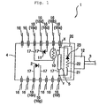
- FIG. 1 shows an example of electric wiring characteristic of a semiconductor laser module according to the first embodiment of the invention.
- a characteristic point resides in that, as shown in FIG. 1, an overcurrent limiting circuit 20 which is an overcurrent limiting means (also functioning as a reverse current flow limiting means) is provided.
- the construction other than the above is similar to the semiconductor laser module illustrated in FIG. 6.
- parts which are identical to those in the semiconductor laser module shown in FIG. 6 are given the same reference numbers, and overlapping description thereof is omitted or simplified.
- thermomodule 5 carries out only a cooling action.
- an overcurrent limiting circuit 20 as shown below is provided in a package 4.
- the overcurrent limiting circuit 20 is comprising a bypass line 21, a resistor 22, and a diode 23.
- one end side of the bypass line 21 is connected to point X at the lead pin 16a side from the thermomodule 5, and the other end side of the bypass line 21 is connected to point Y at the lead pin 16f side from the thermomodule 5.
- the first embodiment is constructed so that the thermomodule 5 carries out a heating action, when a current flows in a direction from the lead pin 16f through the lead pin 16a, and so that the thermomodule 5 carries out a cooling action, when current flows in the direction from the lead pin 16a through the lead pin 16f.
- the bypass line 21 is provided to connect the upstream side Y and downstream side X of the thermomodule 5 in the current flow channel in the heating direction of the thermomodule 5, bypassing the thermomodule 5.
- the semiconductor laser module 1 shown in the first embodiment is constructed as described above.
- a brief description is given of examples of circuit operation of the abovementioned overcurrent limiting circuit 20.
- the semiconductor laser module is electrically connected to a drive controlling means for driving the semiconductor laser module, through lead pins 16.
- thermomodule reverse current
- the diode 23 is turned on, whereby a current in the heating direction is shunted to the thermomodule 5 and bypass path 21 in proportion to the ratio of the resistance value of the thermomodule 5 to that of the resistor 22.
- the overcurrent is shunted into the thermomodule 5 and bypass line 21 as described above, whereby, in comparison with a case where all the overcurrent flows into the thermomodule 5, the overcurrent flowing into the thermomodule 5 can be relieved.
- the resistance value of the resistor 22 may be adequately established in compliance with specifications.
- the substrate (plate member (herein, the plate member 5c)) of the thermomodule 5 at the side where a semiconductor laser element is disposed is thermally isolated from the sidewall of the package 4 and the optical fiber supporting member 12. Therefore, in the circuit configuration of the prior art example shown in FIG. 6(b), when an overcurrent flows to the thermomodule 5 in the heating direction, high temperature heat of the thermomodule 5 resulting from the overcurrent is not discharged to the outside of the package 4 via the sidewall thereof and the optical fiber supporting member 12, leading to the heat accumlation in components on the thermomodule 5 and likely to various problems arising therefrom.
- the overcurrent limiting circuit 20 is provided, by which a reverse overcurrent flow to the thermomodule 5 in the heating direction may be relieved (limited). Therefore, it is possible to evade various problems resulting from the overcurrent flow to the thermomodule 5 in the heating direction.
- the semiconductor laser element 2 can be prevented from being heated to a high temperature. Accordingly, the growth of defects in crystal of the semiconductor laser element 2 due to the high temperature heating can be prevented from occurring, whereby it is possible to prevent the characteristics of the semiconductor laser element 2 from deteriorating.
- thermomodule 5 it is possible to prevent a thermal fusion connecting material such as solder, by which a substrate 6 being a member for attaching a semiconductor laser element 2 and components such as lens 9, etc., is connected to the thermomodule 5, from being melted as a result of high temperature heating of the thermomodule 5, whereby it is possible to prevent the substrate 6 from shifting in position. Therefore, since the positional shift of the semiconductor laser element 2 and lens 9 with respect to the optical fiber 3 can be evaded, an optical decoupling (misalignment) between the optical fiber 3 and the semiconductor laser element 2 can be prevented from occurring, thereby preventing a lowering of optical output.
- a thermal fusion connecting material such as solder
- thermomodule 5 it is possible to prevent generation of cracks at the joint between the lens 9 and metallic holder which originates from a quick temperature rise at the substrate 5c side of the thermomodule 5. Thereby, it is possible to prevent the coming off of a lens 9 originated from the generation of cracks , and to avoid such asituation where the optical coupling of the semiconductor laser element 2 and optical fiber 3 may be disrupted.
- thermomodule 5 itself can be avoided.
- thermomodule 5 As described above, by providing an overcurrent limiting circuit 20 which is characteristic in the first embodiment, it is possible to prevent various problems from occurring due to a reverse overcurrent flowing into the thermomodule 5 in the heating direction. Therefore, optical coupling, durability and reliability of a semiconductor laser module 1 can be remarkably improved.
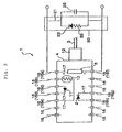
- thermomodule 5 A characteristic point at which the second embodiment differs from the abovementioned first embodiment resides in that, as shown in FIG. 2, a capacitor 25 for a surge current flow is provided in parallel to the thermomodule 5. The construction other than this is similar to that of the first embodiment.
- parts which are identical to those in the first embodiment are given the same reference numbers, and overlapping description thereof is omitted.
- thermomodule 5 since the capacitor 25 is provided in parallel to the thermomodule 5, no surge current, which is an instantaneous large current, is allowed to flow into the thermomodule 5 since the surge current flows into the capacitor 25 should any surge current occur. Therefore, it is possible to prevent the thermomodule 5 from being damaged due to any surge current flow.
- thermomodule 5 the frequency of a surge current is high, and the higher the frequency becomes in a capacitor, the smaller the impedance thereof becomes. Therefore, even though a surge current is generated and tries to enter the thermomodule 5, almost all of the surge current will flow into the capacitor 25, whereby it is possible to suppress the surge current from flowing into the thermomodule 5, and to prevent the thermomodule from being damaged due to the surge current. Also, there is a fear that components on the thermomodule 5 will be subjected to a quick temperature rise and various problems occur as described above if a surge current flows into the thermomodule 5 in the heating direction.
- thermomodule 5 Such a surge current flow to the thermomodule 5 can be prevented by the capacitor 25 in the second embodiment as described above, and therefore, various problems such as deterioration of the characteristics of the semiconductor laser element 2, an optical decoupling between the semiconductor laser element 2 and the optical fiber 3, and disruption of the optical coupling due to a coming-off of a lens, can be securely prevented from occurring.
- thermomodule 5 since an overcurrent limiting circuit 20 is provided, it is possible to suppress (limit) a reverse overcurrent flow to the thermomodule 5 in the heating direction by the abovementioned overcurrent limiting circuit 20 as in the first embodiment whereby various problems arising from the overcurrent flow in the heating direction can be prevented. Furthermore, as described above, since the capacitor 25 is provided in parallel to the thermomodule 5, the capacitor 25 can prevent various problems from occurring due to a surge current flow.
- the invention is not limited to the abovementioned respective embodiments, but it may be subjected to various modifications or embodiments.
- the thermomodule 5 taking into consideration a case where a semiconductor laser module 1 is used not only at a ambient temperature higher than normal but also at (ambient temperature) lower (than normal), it was assumed that the thermomodule 5 carries out not only a cooling action but also a heating action. Therefore, in order to feed a current (reverse current) to the thermomodule 5 in the heating direction, a resistor 22 was interposed in the bypass line 21.
- the semiconductor laser module 1 is used only at ambient temperature higher than normal, that is, where it is assumed that the thermomodule 5 carries out only a cooling action, there may be no need to provide the resistor 22.
- thermomodule carries out only a cooling action, and therefore it is not necessary to feed a current (reverse current) to the thermomodule 5 in the heating direction
- a diode in which the current direction for cooling is made into a forward direction may be provided in series for the thermomodule 5 as a reverse current flow prevention means with no bypass line 21 provided. That is, it may be constructed so that the current flowing into the thermomodule 5 in the heating direction is completely prevented by the diode.
- an example is illustrated of a semiconductor laser module with an overcurrent flow limiting feature, in which the abovementioned overcurrent limiting circuit 20 is provided in the package 4.
- an overcurrent limiting circuit 20 consisting of a bypass line 21, a resistor 22, and a diode 23, which are covered by a dashed line in Fig. 3, maybe provided between a semiconductor laser module 1 having a similar construction to the prior art (construction shown in FIG. 6) and a drive controlling means for the semiconductor laser module, in order to drive the semiconductor laser module .
- a capacitor 25 similar to that in the second embodiment may be provided outside the semiconductor laser module 1 as shown with a dotted line in FIG. 3.
- the overcurrent limiting means is not limited to an overcurrent limiting circuit 20 consisting of a bypass line 21, a resistor 22, and a diode 23 as illustrated in Fig. 3, but it can be achieved by other circuit means having similar functions or a software means. Further, it is needless to say that effects of the invention can be brought about by using as a drive power source of the Peltier module 5 a power source circuit (power source apparatus) equipped with similar functions .
- a method for driving a semiconductor laser module according to the invention may be applicable to various types of transmission devices incorporating (or equipped with) a semiconductor laser module that controls the temperature of the semiconductor laser element by a Peltier element.
- a semiconductor pumping laser module at the 1480nm and the 980nm band for use in a high output optical fiber amplifier generates much heat, at the semiconductor laser element, and is mostly used in high temperature environment, a current flown into the Peltier module to cool down the semiconductor laser element is very large. Therefore, a method for driving a semiconductor laser module according to the invention is favorable as a method for driving a semiconductor laser module in an optical fiber amplifier.
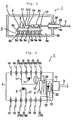
- a coupling optical system is formed of discrete lenses 9 and 14 from the optical fiber 3 as shown in FIG. 6(a), it may be formed of a lensed optical fiber 3 without utilizing the (discrete) lenses 9 and 14 as shown in Fig. 4.
- the lensed optical fiber 3 is an optical fiber having a lens 3a for focussing laser light emitted from a semiconductor laser element 2.
- the lensed optical fiber 3 is incorporated in the semiconductor laser module 1 as described below.
- a fixing member 27 for example, made of stainless steel
- an optical fiber supporting member 28 is fixed at the fixing member 27 by YAG laser welding, etc.
- another optical fiber supporting member 29 is fitted into and attached in a through hole 4c formed at the package 4 and is fixed therein by a connection material 30 such as PbSn solder, etc.
- the optical fiber supporting members 28 and 29 are, respectively, provided with a through hole though which an optical fiber 3 is introduced from outside of the package 4 into the inside thereof with the tip of the optical fiber and the semiconductor laser element 2 being disposed with an adequate spacing to be optically coupled to each other. Constructions other than the above are similar to those shown in FIG. 6(a), and overlapping description thereof is omitted herein.
- the optical fiber supporting members 28 and 29 are constructed of, for example, a thermally conductive material such as, for example, Fe-Ni-Co alloy, etc. Strictly speaking, in the construction shown in FIG. 4, a substrate (that is, a plate member 5c) of the thermomodule 2 at the side where the semiconductor laser element 2 is disposed is thermally connected to the optical fiber supporting member 29 via the optical fiber 3. But, since the optical fiber 3 is made of quartz glass having a very thin diameter of 125 ⁇ m or so, the quantity of heat transmitted from the plate member 5c of the thermomodule 5 to the optical fiber supporting member 29 via the optical fiber 3 is very slight.
- the plate member 5c of the thermomodule 5 is thermally isolated from the abovementioned optical fiber supporting member 29. That is, the configuration shown in FIG. 4 is such that discharge of heat from the plate member 5c of the thermomodule 5 to the outside of the package 4 via the optical fiber supporting member 29 is limited.
- an electric wiring configuration shown in FIG. 6 is employed when discharge of the heat is limited, high temperature heat is accumulated in components on the thermomodule 5 and causes various problems if the thermomodule 5 is heated to an extraordinarily high temperature due to an overcurrent flow to the thermomodule 5.
- the semiconductor laser module with a construction for suppressing an overcurrent flow to the thermomodule 5 as shown in the abovementioned respective embodiments, various problems resulting from the overcurrent flow to the thermomodule 5 can be effectively prevented from occurring.
- FIG. 5 a construction shown in FIG. 5 is proposed as still another embodiment of the invention.
- the example shown in FIG. 5 does not correspond to current control with respect to the thermomodule 5, but it corresponds to voltage control with respect to the thermomodule 5. That is, with this construction, it is possible to avoid problems that result from the application of overvoltage to the thermomodule 5.
- an overvoltage limiting means 31 is provided in series with respect to the thermomodule 5.
- the overvoltage limiting means 31 is composed of a parallel connection body consisting of a diode 32 in which the current flow direction in the cooling direction is made forward to be, and a resistor 33.
- thermomodule 5 when voltage in the cooling direction is applied to the thermomodule 5, the diode 32 turns on, wherein almost no current flows into the resistor 33, while almost all current flows in the diode 32. Thereby, almost all voltage applied between the lead pins 16a and 16f is applied to the thermomodule 5.
- thermomodule 5 when voltage in the heating direction is applied to the thermomodule 5, the diode 32 turns off, wherein the current flows into the resistor 33, and the voltage applied between the lead pin 16a and 16f is divided to be applied to the thermomodule 5 and resistor 3. Based thereon, where overvoltage occurs between the lead pins 16a and 16f occurs, the overvoltage is divided to be applied to the thermomodule 5 and the resistor 33. Therefore, it is possible to relieve (limit) the overvoltage application onto the thermomodule 5, and to prevent various problems arising from the application of overvoltage to the thermomodule 5. Any one or both of such overvoltage limiting means and an overcurrent limiting means shown with respect to the abovementioned respective embodiments may be provided in a semiconductor laser module according to the invention.
- a semiconductor laser module and a method for driving the semiconductor laser module according to the invention is capable of preventing the semiconductor laser and its related components from deteriorating or being damaged, circuit operations from becoming unstable, and the optical system from the semiconductor laser to an optical fiber from misaligning, all of which result from excessive heating, etc., by suppressing overcurrent and overvoltage. Therefore, they are suitable as a means for carrying out highly reliable optical transmissions.
Landscapes
- Physics & Mathematics (AREA)
- Condensed Matter Physics & Semiconductors (AREA)
- General Physics & Mathematics (AREA)
- Electromagnetism (AREA)
- Optics & Photonics (AREA)
- Optical Couplings Of Light Guides (AREA)
- Semiconductor Lasers (AREA)
Abstract
Description
Claims (13)
- A semiconductor laser module comprising a semiconductor laser element, a thermomodule for adjusting the temperature of the semiconductor laser element, an optical fiber optically coupled to laser light emitted from the semiconductor laser element,
wherein said thermomodule is constructed so as to variably adjust the temperature of a semiconductor laser in compliance with the amount of a current flowing into said thermomodule, and any one or both of an overcurrent limiting means to suppress an overcurrent flowing into the thermomodule, and an overvoltage limiting means to suppress overvoltage application onto said thermomodule is provided. - A semiconductor laser module as set forth in Claim 1, wherein a reverse current flow prevention means which prevents a current from flowing into said thermomodule in a direction opposite to that of a drive current of said thermomodule is provided.
- A semiconductor laser module as set forth in Claim 1, wherein said thermomodule is constructed so that it can change the heating action and the cooling action in compliance with the orientation of the flowing current, and said overcurrent limiting means is connected to a current flowing channel by which a current in the heating direction to cause said thermomodule to carry out a heating action is permitted to flow.
- A semiconductor laser module as set forth in Claim 3, wherein said current flowing channel by which a current in the heating direction is flown is provided with a bypass channel by which the upstream side and downstream side of said thermomodule are connected to each other, bypassing the thermomodule, and a resistor intervenes in the bypass channel, and at the same time, a diode in which the current direction for heating is made to be a forward direction is provided in series with the resistor;
wherein said bypass channel, resistor and diode are constructed as an overcurrent limiting means to relieve the flow of an overcurrent in the heating direction into said thermomodule by shunting the current in the heating direction to said thermomodule and bypass channel. - A semiconductor laser module as set forth in any one of Claims 1 through 4, wherein said thermomodule is constructed by placing Peltier elements between the first substrate and second substrate, a semiconductor laser element is disposed at any one of said first substrate and said second substrate, and is thermally connected to said thermomodule, and a lens is provided to focuss laser light emitted from the semiconductor laser and to introduce said laser light into an optical fiber, wherein said lens is thermally connected to a substrate of said thermomodule at the side at which a semiconductor laser element is disposed, via a thermally melting connection material by which a member for attaching said lens is fixed.
- A semiconductor laser module as set forth in any one of Claims 1 through 4, wherein said optical fiber is a lensed optical fiber in which a lens to condense laser light emitted from said semiconductor laser element is formed at the tip end portion into which laser light is made incident.
- A semiconductor laser module as set forth in any one of Claims 1 through 4, wherein said thermomodule is constructed by placing Peltier elements between the first substrate and the second substrate, and a semiconductor element is disposed on any one of the first substrate and the second substrate and is thermally connected to the thermomodule,
wherein said semiconductor laser element and thermomodule are disposed and accommodated in a package which is provided with a through hole communicating from the inside of said package to the outside thereof, an optical fiber supporting member consisting of a thermally conducting member is inserted into and fitted in said through hole, the end portion side of an optical fiber is introduced from the outside of said package into the inside thereof via a through hole provided in said optical fiber supporting member, the substrate of said thermomodule at the side at which a semiconductor laser element is disposed is thermally isolated from said optical fiber supporting member, and discharge of heat from the substrate of said thermomodule at the side at which the semiconductor laser element is disposed, to the outside of the package via the optical fiber supporting member is limited. - A semiconductor laser module as set forth in Claim 5, wherein said thermomodule is constructed by placing Peltier elements between the first substrate and the second substrate, and a semiconductor element is disposed on any one of the first substrate and the second substrate and is thermally connected to the thermomodule,
wherein said semiconductor laser element and thermomodule are disposed and accommodated in a package which is provided with a through hole communicating from the inside of said package to the outside thereof, an optical fiber supporting member consisting of a thermally conducting material is inserted into and fitted in said through hole, the end portion side of an optical fiber is introduced from the outside of said package into the inside thereof via a through hole provided in said optical fiber supporting member, the substrate of said thermomodule at the side at which a semiconductor laser element is disposed, is thermally isolated from said optical fiber supporting member, and discharge of heat from the substrate of said thermomodule at the side at which the semiconductor laser element is disposed, to the outside of the package via the optical fiber supporting member is limited. - A semiconductor laser module as set forth in any one of Claim 6, wherein said thermomodule is constructed by placing Pettier elements between the first substrate and the second substrate, and a semiconductor element is disposed on any one of the first substrate and the second substrate and is thermally connected to the thermomodule,
wherein said semiconductor laser element and thermomodule are disposed and accommodated in a package which is provided with a through hole communicating from the inside of said package to the outside thereof, an optical fiber supporting member consisting of a thermally conducting material is inserted into and fitted in said through hole, the end portion side of an optical fiber is introduced from the outside of said package into the inside thereof via a through hole provided in said optical fiber supporting member, the substrate of said thermomodule at the side at which a semiconductor laser element is disposed, is thermally isolated from said optical fiber supporting member, and discharge of heat from the substrate of said thermomodule at the side at which the semiconductor laser element of said thermomodule is disposed, to the outside of the package via the optical fiber supporting member is limited. - A method for driving a semiconductor laser module having a semiconductor laser element, a thermomodule for adjusting the temperature of the semiconductor laser element, and an optical fiber optically coupled to laser light emitted from said semiconductor laser element, comprising the steps of:thermally connecting said thermomodule to said semiconductor laser element;adjusting the temperature of the semiconductor laser element in compliance with the amount of a current flowing into the thermomodule; andsuppressing the overcurrent flow into the thermomodule by providing an overcurrent flow limiting means in a current flow channel to the thermomodule.
- A method for driving a semiconductor laser module having a semiconductor laser element, a thermomodule for adjusting the temperature of said semiconductor laser element, and an optical fiber optically coupled to laser light emitted from the semiconductor laser element, wherein said thermomodule is constructed so that it changes the heating action and the cooling action in response to the orientation of a current flow; comprising the steps of:thermally connecting said thermomodule to a semiconductor laser element;providing a current path, by which a current is supplied in the heating direction to cause said thermomodule to carry out a heating action, with a bypass channel which connects the upstream side and downstream side of said thermomodule, bypassing said thermomodule;interposing a resistor in the bypass channel, andrelieving the overcurrent flow to said thermomodule in the heating direction by shunting the current in the heating direction to said thermomodule and bypass channel.
- A transmission device comprising a semiconductor laser module having a semiconductor laser element, a thermomodule for adjusting the temperature of said semiconductor laser element, and an optical fiber optically coupled to laser light emitted from said semiconductor laser element; wherein said thermomodule is constructed so that it variably adjusts the temperature of a semiconductor laser element in compliance with the amount of a current flowing into said thermomodule, and wherein any one or both of an overcurrent limiting means which suppresses an overcurrent from flowing into said thermomodule, and an overvoltage limiting means which suppresses overvoltage from being applied to said thermomodule is provided.
- A transmission device as set forth in Claim 12, wherein any one or both of said overcurrent limiting means and overvoltage limiting means is or are provided in a power source apparatus.
Applications Claiming Priority (3)
| Application Number | Priority Date | Filing Date | Title |
|---|---|---|---|
| JP31099299 | 1999-11-01 | ||
| JP31099299A JP3469833B2 (en) | 1998-11-19 | 1999-11-01 | Semiconductor laser module, overcurrent limiting circuit therefor, and method of driving semiconductor laser module |
| PCT/JP2000/003147 WO2001033680A1 (en) | 1999-11-01 | 2000-05-17 | Semiconductor laser module and method of driving semiconductor laser module |
Publications (3)
| Publication Number | Publication Date |
|---|---|
| EP1146613A1 true EP1146613A1 (en) | 2001-10-17 |
| EP1146613A4 EP1146613A4 (en) | 2006-07-05 |
| EP1146613B1 EP1146613B1 (en) | 2010-06-23 |
Family
ID=18011842
Family Applications (1)
| Application Number | Title | Priority Date | Filing Date |
|---|---|---|---|
| EP00927782A Expired - Lifetime EP1146613B1 (en) | 1999-11-01 | 2000-05-17 | Semiconductor laser module and method of driving semiconductor laser module |
Country Status (3)
| Country | Link |
|---|---|
| EP (1) | EP1146613B1 (en) |
| CA (1) | CA2358441C (en) |
| DE (1) | DE60044577D1 (en) |
Cited By (1)
| Publication number | Priority date | Publication date | Assignee | Title |
|---|---|---|---|---|
| EP1168537A1 (en) * | 2000-06-22 | 2002-01-02 | The Furukawa Electric Co., Ltd. | Semiconductor laser module, and method for driving the semiconductor laser module |
Family Cites Families (1)
| Publication number | Priority date | Publication date | Assignee | Title |
|---|---|---|---|---|
| JPS58176988A (en) * | 1982-04-09 | 1983-10-17 | Olympus Optical Co Ltd | Semiconductor laser temperature control apparatus |
-
2000
- 2000-05-17 EP EP00927782A patent/EP1146613B1/en not_active Expired - Lifetime
- 2000-05-17 CA CA2358441A patent/CA2358441C/en not_active Expired - Fee Related
- 2000-05-17 DE DE60044577T patent/DE60044577D1/en not_active Expired - Lifetime
Cited By (1)
| Publication number | Priority date | Publication date | Assignee | Title |
|---|---|---|---|---|
| EP1168537A1 (en) * | 2000-06-22 | 2002-01-02 | The Furukawa Electric Co., Ltd. | Semiconductor laser module, and method for driving the semiconductor laser module |
Also Published As
| Publication number | Publication date |
|---|---|
| CA2358441C (en) | 2010-03-30 |
| EP1146613A4 (en) | 2006-07-05 |
| DE60044577D1 (en) | 2010-08-05 |
| CA2358441A1 (en) | 2001-05-10 |
| EP1146613B1 (en) | 2010-06-23 |
Similar Documents
| Publication | Publication Date | Title |
|---|---|---|
| US5068865A (en) | Semiconductor laser module | |
| JP3488159B2 (en) | Alignment device for light source and optical fiber and light source module having the same | |
| CN102043208B (en) | Cooled laser module | |
| US7011457B2 (en) | Optical coupling apparatus | |
| US5706302A (en) | Temperature control type semiconductor laser device | |
| US20060022213A1 (en) | TO-can heater on flex circuit | |
| JP4087190B2 (en) | OPTICAL DEVICE, OPTICAL DEVICE START-UP METHOD AND DRIVE METHOD, AND OPTICAL COMMUNICATION DEVICE | |
| EP1146613B1 (en) | Semiconductor laser module and method of driving semiconductor laser module | |
| US6385222B1 (en) | Semiconductor laser module, and method for driving the semiconductor laser module | |
| JP3469833B2 (en) | Semiconductor laser module, overcurrent limiting circuit therefor, and method of driving semiconductor laser module | |
| US20050117231A1 (en) | Optical transmission module with temperature control | |
| US6996145B2 (en) | Semiconductor laser module, and method for driving the semiconductor laser module | |
| CA2351260C (en) | Semiconductor laser module, and method for driving the semiconductor laser module | |
| JP2016004989A (en) | Optical communication package and optical module | |
| JP3938496B2 (en) | Driving method of semiconductor laser module | |
| JP2002009383A (en) | Semiconductor laser module and thermo module | |
| JP4043886B2 (en) | Semiconductor laser device start-up method and optical communication device using semiconductor laser device | |
| JP3566911B2 (en) | Semiconductor laser module, method of driving the same, overcurrent limiting circuit, and communication device using semiconductor laser module | |
| JP3858001B2 (en) | Semiconductor laser module and driving method of semiconductor laser module | |
| JPH0452636B2 (en) | ||
| JP3938497B2 (en) | Optical communication equipment with semiconductor laser module | |
| WO2001033680A1 (en) | Semiconductor laser module and method of driving semiconductor laser module | |
| KR0121330B1 (en) | Semiconductor laser module optical | |
| JP2007025433A (en) | Optical element module and optical transmitter | |
| JPH10300988A (en) | Optical module |
Legal Events
| Date | Code | Title | Description |
|---|---|---|---|
| PUAI | Public reference made under article 153(3) epc to a published international application that has entered the european phase |
Free format text: ORIGINAL CODE: 0009012 |
|
| 17P | Request for examination filed |
Effective date: 20010525 |
|
| AK | Designated contracting states |
Kind code of ref document: A1 Designated state(s): AT BE CH CY DE DK ES FI FR GB GR IE IT LI LU MC NL PT SE |
|
| RBV | Designated contracting states (corrected) |
Designated state(s): DE FR GB IT |
|
| A4 | Supplementary search report drawn up and despatched |
Effective date: 20060606 |
|
| 17Q | First examination report despatched |
Effective date: 20080429 |
|
| GRAP | Despatch of communication of intention to grant a patent |
Free format text: ORIGINAL CODE: EPIDOSNIGR1 |
|
| RIN1 | Information on inventor provided before grant (corrected) |
Inventor name: AIKIYO, TAKESHI,THE FURUKAWA ELECTRIC CO., LTD. |
|
| RAP1 | Party data changed (applicant data changed or rights of an application transferred) |
Owner name: THE FURUKAWA ELECTRIC CO., LTD. |
|
| GRAS | Grant fee paid |
Free format text: ORIGINAL CODE: EPIDOSNIGR3 |
|
| GRAA | (expected) grant |
Free format text: ORIGINAL CODE: 0009210 |
|
| AK | Designated contracting states |
Kind code of ref document: B1 Designated state(s): DE FR GB IT |
|
| REF | Corresponds to: |
Ref document number: 60044577 Country of ref document: DE Date of ref document: 20100805 Kind code of ref document: P |
|
| PG25 | Lapsed in a contracting state [announced via postgrant information from national office to epo] |
Ref country code: IT Free format text: LAPSE BECAUSE OF FAILURE TO SUBMIT A TRANSLATION OF THE DESCRIPTION OR TO PAY THE FEE WITHIN THE PRESCRIBED TIME-LIMIT Effective date: 20100623 |
|
| PLBE | No opposition filed within time limit |
Free format text: ORIGINAL CODE: 0009261 |
|
| STAA | Information on the status of an ep patent application or granted ep patent |
Free format text: STATUS: NO OPPOSITION FILED WITHIN TIME LIMIT |
|
| 26N | No opposition filed |
Effective date: 20110324 |
|
| REG | Reference to a national code |
Ref country code: DE Ref legal event code: R097 Ref document number: 60044577 Country of ref document: DE Effective date: 20110323 |
|
| REG | Reference to a national code |
Ref country code: DE Ref legal event code: R119 Ref document number: 60044577 Country of ref document: DE Effective date: 20111201 |
|
| PG25 | Lapsed in a contracting state [announced via postgrant information from national office to epo] |
Ref country code: DE Free format text: LAPSE BECAUSE OF NON-PAYMENT OF DUE FEES Effective date: 20111201 |
|
| REG | Reference to a national code |
Ref country code: FR Ref legal event code: PLFP Year of fee payment: 16 |
|
| PGFP | Annual fee paid to national office [announced via postgrant information from national office to epo] |
Ref country code: GB Payment date: 20150513 Year of fee payment: 16 |
|
| PGFP | Annual fee paid to national office [announced via postgrant information from national office to epo] |
Ref country code: FR Payment date: 20150508 Year of fee payment: 16 |
|
| GBPC | Gb: european patent ceased through non-payment of renewal fee |
Effective date: 20160517 |
|
| REG | Reference to a national code |
Ref country code: FR Ref legal event code: ST Effective date: 20170131 |
|
| PG25 | Lapsed in a contracting state [announced via postgrant information from national office to epo] |
Ref country code: FR Free format text: LAPSE BECAUSE OF NON-PAYMENT OF DUE FEES Effective date: 20160531 |
|
| PG25 | Lapsed in a contracting state [announced via postgrant information from national office to epo] |
Ref country code: GB Free format text: LAPSE BECAUSE OF NON-PAYMENT OF DUE FEES Effective date: 20160517 |