EP1146395A2 - Lithographic apparatus, device manufacturing method, and device manufactured by said method - Google Patents
Lithographic apparatus, device manufacturing method, and device manufactured by said method Download PDFInfo
- Publication number
- EP1146395A2 EP1146395A2 EP01303299A EP01303299A EP1146395A2 EP 1146395 A2 EP1146395 A2 EP 1146395A2 EP 01303299 A EP01303299 A EP 01303299A EP 01303299 A EP01303299 A EP 01303299A EP 1146395 A2 EP1146395 A2 EP 1146395A2
- Authority
- EP
- European Patent Office
- Prior art keywords
- substrate
- support structure
- wafer
- radiation
- level sensor
- Prior art date
- Legal status (The legal status is an assumption and is not a legal conclusion. Google has not performed a legal analysis and makes no representation as to the accuracy of the status listed.)
- Granted
Links
Images




Classifications
-
- G—PHYSICS
- G03—PHOTOGRAPHY; CINEMATOGRAPHY; ANALOGOUS TECHNIQUES USING WAVES OTHER THAN OPTICAL WAVES; ELECTROGRAPHY; HOLOGRAPHY
- G03F—PHOTOMECHANICAL PRODUCTION OF TEXTURED OR PATTERNED SURFACES, e.g. FOR PRINTING, FOR PROCESSING OF SEMICONDUCTOR DEVICES; MATERIALS THEREFOR; ORIGINALS THEREFOR; APPARATUS SPECIALLY ADAPTED THEREFOR
- G03F9/00—Registration or positioning of originals, masks, frames, photographic sheets or textured or patterned surfaces, e.g. automatically
- G03F9/70—Registration or positioning of originals, masks, frames, photographic sheets or textured or patterned surfaces, e.g. automatically for microlithography
- G03F9/7003—Alignment type or strategy, e.g. leveling, global alignment
- G03F9/7023—Aligning or positioning in direction perpendicular to substrate surface
- G03F9/7034—Leveling
-
- G—PHYSICS
- G03—PHOTOGRAPHY; CINEMATOGRAPHY; ANALOGOUS TECHNIQUES USING WAVES OTHER THAN OPTICAL WAVES; ELECTROGRAPHY; HOLOGRAPHY
- G03F—PHOTOMECHANICAL PRODUCTION OF TEXTURED OR PATTERNED SURFACES, e.g. FOR PRINTING, FOR PROCESSING OF SEMICONDUCTOR DEVICES; MATERIALS THEREFOR; ORIGINALS THEREFOR; APPARATUS SPECIALLY ADAPTED THEREFOR
- G03F7/00—Photomechanical, e.g. photolithographic, production of textured or patterned surfaces, e.g. printing surfaces; Materials therefor, e.g. comprising photoresists; Apparatus specially adapted therefor
- G03F7/70—Microphotolithographic exposure; Apparatus therefor
- G03F7/70216—Mask projection systems
- G03F7/70358—Scanning exposure, i.e. relative movement of patterned beam and workpiece during imaging
Definitions
- the present invention relates to the control of leveling, for example of the substrate and/or mask, during exposures in lithographic apparatus. More particularly, the invention relates to a system for leveling control in a lithographic projection apparatus comprising:
- Lithographic projection apparatus can be used, for example, in the manufacture of integrated circuits (ICs).
- the patterning means may generate a circuit pattern corresponding to an individual layer of the IC, and this pattern can be imaged onto a target portion (e.g. comprising one or more dies) on a substrate (silicon wafer) that has been coated with a layer of radiation-sensitive material (resist).
- a target portion e.g. comprising one or more dies
- a substrate silicon wafer
- a layer of radiation-sensitive material resist
- a single wafer will contain a whole network of adjacent target portions that are successively irradiated via the projection system, one at a time.
- employing patterning by a mask on a mask table a distinction can be made between two different types of machine.
- each target portion is irradiated by exposing the entire mask pattern onto the target portion in one go; such an apparatus is commonly referred to as a wafer stepper.
- a wafer stepper In an alternative apparatus ⁇ commonly referred to as a step-and-scan apparatus ⁇ each target portion is irradiated by progressively scanning the mask pattern under the projection beam in a given reference direction (the "scanning" direction) while synchronously scanning the substrate table parallel or anti-parallel to this direction; since, in general, the projection system will have a magnification factor M (generally ⁇ 1), the speed V at which the substrate table is scanned will be a factor M times that at which the mask table is scanned. More information with regard to lithographic devices as here described can be gleaned, for example, from US 6,046,792, incorporated herein by reference.
- a pattern (e.g. in a mask) is imaged onto a substrate that is at least partially covered by a layer of radiation-sensitive material (resist).
- the substrate Prior to this imaging step, the substrate may undergo various procedures, such as priming, resist coating and a soft bake. After exposure, the substrate may be subjected to other procedures, such as a post-exposure bake (PEB), development, a hard bake and measurement/inspection of the imaged features.
- PEB post-exposure bake
- This array of procedures is used as a basis to pattern an individual layer of a device, e.g. an IC.
- Such a patterned layer may then undergo various processes such as etching, ion-implantation (doping), metallization, oxidation, chemo-mechanical polishing, etc., all intended to finish off an individual layer. If several layers are required, then the whole procedure, or a variant thereof, will have to be repeated for each new layer. Eventually, an array of devices will be present on the substrate (wafer). These devices are then separated from one another by a technique such as dicing or sawing, whence the individual devices can be mounted on a carrier, connected to pins, etc.
- the projection system may hereinafter be referred to as the "lens"; however, this term should be broadly interpreted as encompassing various types of projection system, including refractive optics, reflective optics, and catadioptric systems, for example.
- the radiation system may also include components operating according to any of these design types for directing, shaping or controlling the projection beam of radiation, and such components may also be referred to below, collectively or singularly, as a "lens”.
- the lithographic apparatus may be of a type having two or more substrate tables (and/or two or more mask tables). In such "multiple stage” devices the additional tables may be used in parallel, or preparatory steps may be carried out on one or more tables while one or more other tables are being used for exposures. Twin stage lithographic apparatus are described, for example, in US 5,969,441 and WO 98/40791, incorporated herein by reference.
- lithographic apparatus contained a single mask table and a single substrate table.
- machines are now becoming available in which there are at least two independently moveable substrate tables; see, for example, the multi-stage apparatus described in International Patent Applications WO98/28665 and WO98/40791.
- the basic operating principle behind such multi-stage apparatus is that, while a first substrate table is at the exposure position underneath the projection system for exposure of a first substrate located on that table, a second substrate table can run to a loading position, discharge a previously exposed substrate, pick up a new substrate, perform some initial measurements on the new substrate and then stand ready to transfer the new substrate to the exposure position underneath the projection system as soon as exposure of the first substrate is completed; the cycle then repeats.
- the same principle could be used with just one substrate table which is moved between exposure and measurement positions.
- An object of the present invention is to provide a control system capable of improved "on-the-fly" leveling (that is leveling based on position measurements made during the exposure rather than in advance) performed on a substrate or mask in a lithographic projection apparatus during exposure processes and in particular to reduce focussing errors, cross-talk between tilts and horizontal shifts and unnecessary object table movements.
- a lithographic projection apparatus as specified in the opening paragraph, characterized by a filter connected between said level sensor and said servo system for filtering said position signal.
- the present invention by interposing a filter between the level sensor and the servo system for leveling, enables improvements in the leveling performance. In particular, undesirable movements to follow high spatial frequency (height) variations in the substrate surface can be avoided. Also, trade-offs between performance in different degrees of freedom can be made, especially to avoid cross-talk into horizontal displacements of the substrate which would result in overlay errors.
- the level sensor optionally in cooperation with a position sensor such as an interferometer or a Linear Variable Differential Transformer (LVDT) measurement system, generates a setpoint which the servo system aims to follow. The filter then filters that setpoint.
- LVDT Linear Variable Differential Transformer
- a device manufacturing method comprising the steps of:
- UV radiation e.g. with a wavelength of 365, 248, 193, 157 or 126 nm
- EUV or XUV radiation e.g. having a wavelength in the range 5-20 nm
- particle beams such as ion beams or electron beams.
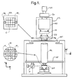
- Figure 1 schematically depicts a lithographic projection apparatus according to a particular embodiment of the invention.
- the apparatus comprises:
- the apparatus is of a transmissive type (i.e. has a transmissive mask). However, in general, it may also be of a reflective type, for example (with a reflective mask). Alternatively, the apparatus may employ another kind of patterning means, such as a programmable mirror array of a type as referred to above.
- the source LA e.g. a Hg lamp, excimer laser, an undulator provided around the path of an electron beam or storage ring or synchrotron, a laser-produced plasma source, a discharge source or an electron or ion beam source
- the illuminator IL may comprise adjusting means AM for setting the outer and/or inner radial extent (commonly referred to as ⁇ -outer and ⁇ -inner, respectively) of the intensity distribution in the beam.
- it will generally comprise various other components, such as an integrator IN and a condenser CO.
- the beam PB impinging on the mask MA has a desired uniformity and intensity distribution in its cross-section.
- the source LA may be within the housing of the lithographic projection apparatus (as is often the case when the source LA is a mercury lamp, for example), but that it may also be remote from the lithographic projection apparatus, the radiation beam which it produces being led into the apparatus (e.g. with the aid of suitable directing mirrors); this latter scenario is often the case when the source LA is an excimer laser.
- the current invention and Claims encompass both of these scenarios.
- the beam PB subsequently intercepts the mask MA, which is held on a mask table MT. Having traversed the mask MA, the beam PB passes through the lens PL, which focuses the beam PB onto a target portion C of the substrate W. With the aid of the second positioning means (and interferometric measuring means IF), the substrate table WT can be moved accurately, e.g. so as to position different target portions C in the path of the beam PB. Similarly, the first positioning means can be used to accurately position the mask MA with respect to the path of the beam PB, e.g. after mechanical retrieval of the mask MA from a mask library, or during a scan.
- the mask table MT may just be connected to a short-stroke actuator, or may be fixed.
- the depicted apparatus can be used in two different modes:
- Unflatness may be caused, for example, by variations in wafer thickness, distortion of the shape of the wafer or contaminants on the wafer table. The presence of structures due to previous process steps also significantly affects the wafer height (flatness). In the present invention, the cause of unflatness is largely irrelevant; only the height of the top surface of the wafer is considered. Unless the context otherwise requires, references below to "the wafer surface” refer to the top surface of the wafer onto which will be projected the mask image.
- the perpendicular, or vertical, position (Z) and parallel, or horizontal, tilts (Rx, Ry) of the wafer table WT are adjusted to keep the wafer surface at the optimal focus position.
- the perpendicular, or vertical, position refers to the position along an axis substantially perpendicular to the plane of the wafer surface
- the parallel, or horizontal, tilts refer to tilts along at least one axis parallel to the plane of the wafer surface.
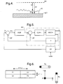
- the detector referred to herein as the level sensor, which may be used for this is shown in Figure 2.
- It comprises a radiation source S which has two emitting areas S1, S2 and supplies two beams, a reference beam and a measurement beam having a wide wavelength band. Also shown are an object grating G1 and an image grating G2. Optical systems (depicted for clarity as simple lenses) L1 and L2 image the object grating G1 onto the image grating G2, the reference beam having been reflected by the outer surface RP of the projection optics PL and the measurement beam by the wafer surface.
- Detectors DE2, DE1 behind the image grating G2 give, when irradiated, signals which can be measured by a meter ME or other suitable instrument, indicative of the relative positions of the points where the reference beam and measurement beam are reflected by the projection optics PL and wafer surface respectively.
- a meter ME or other suitable instrument
- the relative heights of a corresponding number of points on the wafer surface can be measured and local tilts of the wafer surface determined.
- the level sensor is described in greater detail in EP-0 502 583-A and US 5,191,200, for example, which documents are incorporated herein by reference.
- FIG. 3 A schematic of the leveling control system is shown in Figure 3.
- the physical components of the system are the level sensor LS, wafer shape filter WSF and servo system SV.
- the servo system SV is a closed-loop system, including necessary control circuitry, a mechanism for driving the wafer table and a positioning system.
- the level sensor output ls is filtered by the wafer shape filter WSF to give a filtered signal ls' which forms the setpoint of the servo system.
- the servo system drives the wafer table WT to a vertical position vp and may introduce a horizontal servo error hse in the horizontal position of the wafer.
- Such an error can be caused by a non-zero Abbe arm for the Rx and Ry rotations carried out by the servo system, for example.
- the servo system rotates the wafer table about axes not lying exactly on the wafer surface.
- Any error vse in the vertical position signals output by the servo system SV can be measured by subtracting the filtered level sensor signal ls' from the measured vertical position vp ( vp is measured using an interferometer or LVDT, for example).
- vp is measured using an interferometer or LVDT, for example.
- Figure 3 shows general control architectures applicable for all three degrees of freedom Z, Rx and Ry.
- signals such as ls , ls' , Zif , etc., include data of those three degrees of freedom.
- H_aa is the transfer function of element AA in the control system.
- Ztotal is a combination of Z, Rx and Ry errors in such a way that it represents the maximal Z displacement in the radiation system's exposure slit, effectively the maximum Z error on one of the four corners of the slit.
- Ztotal is calculated as Z ⁇ Rx.slitsizeY/2 ⁇ Ry.slitsizeX/2.
- SlitsizeY is defined as the width of said projection beam in a scanning direction of one of the support structure and the wafer table, and slitsizeX refers to a width of said projection beam in a direction substantially perpendicular to the said scanning direction.
- the transfer function H_wsf of the wafer shape filter is determined for each application to provide the desired improvements to the above errors.
- the transfer function H_wsf may be empirically derived to compensate for the divergence of the transfer function H_ls of the actual level sensor LS and so reduces the dynamic measurement error dme to zero.
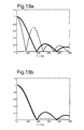
- the ideal level sensor transfer function has a magnitude that decreases with spatial frequency, and a first zero-crossing at a spatial frequency equal to the inverse of the width of the exposure slit in the scan direction (in the case of a step-and-scan apparatus). This is advantageous as it prevents the wafer table attempting to follow variations in the wafer surface of wavelength shorter than the slit width and in particular reduces undesired horizontal movements due to high-frequency cross-talk.
- the wafer shape filter transfer function can also be adjusted to compensate for or compromise between the other errors.
- Appropriate forms for the wafer shape filter transfer function to achieve the desired effects can be derived empirically or by modeling the servo system. For example, in one servo system it was determined that Y errors were out of specification whilst Ztotal and Rx errors were comfortably within limits.
- a notch filter in the Rx wafer shape filter transfer function with a center frequency equal to the peak frequency of the Y moving average error was found to improve Y accuracy at an acceptable cost to Rx and Ztotal.
- the damping coefficients were selected to provide the desired improvement in Y whilst reducing the cost to Rx and Ztotal.
- control system makes use of information indicating the position of the wafer table WT provided by an interferometric displacement measurement system IF.
- interferometric displacement measurement system IF Suitable three, five and six-axis interferometric metrology systems are described in WO99/28790 and WO99/32940, for example, which are incorporated herein by reference.
- An LVDT measurement system may also be used in place of the interferometer. In such a system, three LVDTs are located under the wafer table WT and their outputs transformed to give Z, Rx and Ry data.
- the interferometer system IF measures the position Zif of the wafer table WT (sometimes referred to as the mirror block, as the interferometer system makes use of mirrors bonded to the sides of the wafer table) relative to the focal plane FP of the projection lens system PL whilst the level sensor measures the height ls of the upper surface of the wafer W.
- the interferometer data though denoted simply Zif , includes information regarding the horizontal tilt, Rx and Ry, of the wafer table as well as vertical position, Z.
- the wafer shape filter WSF provides the filtered wafer shape signal ws' which acts as setpoint data for an inner closed-loop control system (within the double dotted line in Figure 5) comprising controller CONT, the short-stroke table drive system MECH, the interferometer IF and a subtractor which subtracts the position of the wafer table as indicated by the interferometer data Zif from the filtered wafer shape data ws '.
- the wafer shape filter WSF acts on the wafer shape data ws (which represents the actual shape of the wafer) rather than the level sensor data (which includes the instantaneous position of the wafer table).
- the inner loop has a high bandwidth, e.g. 50 or 100 Hz or more, and is able to follow the wafer shape setpoint ws' accurately.
- the outer loop determines the setpoint by filtering the wafer shape signal ws .
- the wafer shape filter WSF will therefore not affect the performance of the inner loop.
- the outer loop needs to be stable and to have limited closed-loop amplification.
- the wafer shape filter is selected to correct measurement errors in the level sensor LS and to reduce vertical (tilt) to horizontal crossover.
- a third embodiment of the invention is described with reference to Figures 6 and 7.
- the third embodiment incorporates so-called "look-ahead" in the level sensor LS to compensate for delay which is caused in the wafer shape filter.
- the level sensor including look-ahead is denoted LS' and utilizes a measurement spot pattern as depicted in Figure 6.
- Measurement spots P1 and Q2 are positioned ahead of the center of the projection lens whilst Q1 and P2 are behind.
- the corresponding signals are denoted as ZP1, ZQ2, ZQ1, ZP2, respectively.
- sensor look-ahead for Z and Ry position is effected by weighting the advance spot measurements more heavily than the back spots.
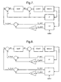
- control system shown in Figure 7 is then essentially the same as that of the second embodiment, shown in Figure 5, save that the level sensor LS' is adapted to provide the gradient signals, and a look-ahead multiplier y_l_a and adder are introduced to generate the sensor look-ahead data.
- the fourth embodiment which is shown in Figure 8, is similar to the third but includes look-ahead in the interferometer IF, or LVDT measurement system, as well.
- This avoids errors in ls_front Z which may occur in the third embodiment when there is a significant Rx tilt.
- the Z level sensor front signal and the Z interferometer signal are not measured at exactly the same spot so that there will be an error in the Z wafer shape signal ws if there is a significant Rx tilt.
- the interferometer gradients for Rx and Ry are defined as zero so that the corresponding look-ahead signals are equal to the center signals.
- control system architecture of a fifth embodiment of the invention is shown in Figure 9. This arrangement is effectively the same as the fourth embodiment but, by subtracting the center and gradient signals before multiplication by y_l_a , one multiplier is saved.
- a sixth embodiment of the invention is shown in Figure 10.
- the sixth embodiment incorporates an additional correction AF_corr to compensate for changes in the position of the actual best focal plane.
- Such changes may be effected deliberately or may be caused by temperature variations in the elements of the projection optical system PL and temperature or pressure variation in the gas or air filling the projection optical system PL.
- a measured or predicted change of the actual focal plane in Z or Ry is automatically compensated for in the level sensor LS' which measures the position of the wafer surface relative to the optimum focal plane.
- a change of the optimum focal plane in Rx will, with sensor look-ahead, result in an error in the Z position of the wafer surface.
- the wafer shape Z value is corrected by - ⁇ Rx.
- ⁇ Rx is the change in the position of the optimum focal plane, or the Z gradient is corrected by - ⁇ R x.
- AF_corr is subtracted from the differential gradient signal if_grad - ls_gra d.
- AF_corr is defined as ⁇ Rx for Z and zero for Rx and Ry.
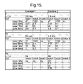
- Example 1 no Rx wafer shape filter was used and the wafer shape filter acts on a time series of values representing heights at positions spaced in the Y (scanning) direction.
- Example 2 an Rx filter was added to the filter of example 1 to improve the Y performance at the expense of Rx performance.
- Simulations were carried out using test data derived from a sample of six test wafers. In the simulations, moving averages (MA) and moving standard deviations (MSD) for servo errors in Ztotal, Z, Rz, Ry, X and Y, as well as dynamic leveling errors in Ztotal, Z, Rx and Ry, were calculated, i.e. a total of 120 values.
- MA moving averages
- MSD moving standard deviations
- Example 1 reduced the number of out-of-spec results from 20 to 11 whilst Example 2 reduced this to 1.
- the wafer shape filter settings of Examples 1 and 2 are based on a scanning speed of 250mm/s.
- the look-ahead distances and filters can be adapted, e.g. so as to maintain a constant look-ahead time, rather than distance.
- the frequency values of the wafer shape filter can be made proportional to scanning speed so that they represent constant spatial frequencies.
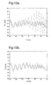
- Figures 11 to 14 show test results obtained using the filter of Example 1 and a test wafer with a special (waved) step topology.
- the surface has a step topology with decreasing wavelength in the Y direction.
- the positive X half is flat.
- Figures 11A and 11B show actual Z position movements (dashed) on this wafer compared to ideal (solid), without and with wafer shape filtering respectively.
- Figures 12A and 12B show actual Ry movements (dashed) compared to ideal (solid), without and with wafer shape filtering respectively.
- Figures 13A and 13B show actual Z level sensor transfer functions (dashed) compared to ideal (solid), without and with wafer shape filtering respectively.
- Figures 14A and 14B show actual Ry level sensor transfer functions (dashed) compared to ideal (solid), without and with wafer shape filtering respectively. It can readily be seen that with the invention the transfer functions and wafer movements are considerably closer to the ideal. In particular, undesirable high-frequency movements of the wafer table are avoided.
- the actual form of the filter will be determined according to the specific embodiment of the invention and the desired performance criteria.
- One approach to selection of a suitable filter is to first find a level sensor look-ahead distance which ensures that the look-ahead transfer function of the level sensor lies above the ideal transfer function, at least up to the first zero-crossing at 1/slitsizeY. Using a two-notch filter, the first notch is then used to shape the transfer function up to the first zero-crossing. The second notch is used to filter off the frequencies higher than the first zero-crossing and to adjust the phase of the transfer function up to the first zero-crossing.
Landscapes
- Physics & Mathematics (AREA)
- General Physics & Mathematics (AREA)
- Exposure And Positioning Against Photoresist Photosensitive Materials (AREA)
- Exposure Of Semiconductors, Excluding Electron Or Ion Beam Exposure (AREA)
Abstract
Description
- a radiation system for supplying a projection beam of radiation;
- a support structure for supporting patterning means, the patterning means serving to pattern the projection beam according to a desired pattern;
- a substrate table for holding a substrate; and
- a projection system for projecting the patterned beam onto a target portion of the substrate;
- a level sensor for measuring at least one of a perpendicular position and tilt about at least one parallel axis of a surface of an object held by one of the support structure and the substrate table, and generating a position signal indicative thereof, perpendicular referring to a direction substantially perpendicular to the said surface and parallel referring to a direction substantially parallel to said surface; and
- a servo system responsive to said position signal for moving said object to a desired position.
- A mask. The concept of a mask is well known in lithography, and it includes mask types such as binary, alternating phase-shift, and attenuated phase-shift, as well as various hybrid mask types. Placement of such a mask in the radiation beam causes selective transmission (in the case of a transmissive mask) or reflection (in the case of a reflective mask) of the radiation impinging on the mask, according to the pattern on the mask. In the case of a mask, the support structure will generally be a mask table, which ensures that the mask can be held at a desired position in the incoming radiation beam, and that it can be moved relative to the beam if so desired.
- A programmable mirror array. An example of such a device is a matrix-addressable surface having a viscoelastic control layer and a reflective surface. The basic principle behind such an apparatus is that (for example) addressed areas of the reflective surface reflect incident light as diffracted light, whereas unaddressed areas reflect incident light as undiffracted light. Using an appropriate filter, the said undiffracted light can be filtered out of the reflected beam, leaving only the diffracted light behind; in this manner, the beam becomes patterned according to the addressing pattern of the matrix-adressable surface. The required matrix addressing can be performed using suitable electronic means. More information on such mirror arrays can be gleaned, for example, from United States Patents US 5,296,891 and US 5,523,193, which are incorporated herein by reference. In the case of a programmable mirror array, the said support structure may be embodied as a frame or table, for example, which may be fixed or movable as required.
- A programmable LCD array. An example of such a construction is given in United States Patent US 5,229,872, which is incorporated herein by reference. As above, the support structure in this case may be embodied as a frame or table, for example, which may be fixed or movable as required.
filtering said position signal before it is used by said servo system to control the position of said object.
These various transfer functions will in general be functions of Z, Rx and Ry and may include terms representing cross-talk into other degrees of freedom. Of these errors, the first four are defined for Z, Rx, Ry and Ztotal, the last only for X and Y. Ztotal is a combination of Z, Rx and Ry errors in such a way that it represents the maximal Z displacement in the radiation system's exposure slit, effectively the maximum Z error on one of the four corners of the slit. Ztotal is calculated as Z ±Rx.slitsizeY/2 ±Ry.slitsizeX/2. SlitsizeY is defined as the width of said projection beam in a scanning direction of one of the support structure and the wafer table, and slitsizeX refers to a width of said projection beam in a direction substantially perpendicular to the said scanning direction.
Claims (15)
- A lithographic projection apparatus comprising:a radiation system for supplying a projection beam of radiation;a support structure for holding patterning means, the patterning means serving to pattern the projection beam according to a desired pattern;a substrate table for holding a substrate; anda projection system for projecting the patterned beam onto a target portion of the substrate;a level sensor for measuring at least one of a perpendicular position and tilt about at least one parallel axis of a surface of an object held by one of the support structure and the substrate table, and generating a position signal indicative thereof, perpendicular referring to a direction substantially perpendicular to the said surface and parallel referring to a direction substantially parallel to said surface; anda servo system responsive to said position signal for moving said object to a desired position; characterized by:
a filter connected between said level sensor and said servo system for filtering said position signal. - Apparatus according to claim 1, wherein the filtered position signal forms a setpoint for said servo system.
- Apparatus according to claim 2, wherein said filter is a low-pass filter arranged to pass components of said position signal having a spatial frequency lower than a predetermined spatial frequency.
- Apparatus according to claim 3, wherein at least one of the support structure and the substrate table are moveable to effect a scanning exposure of a substrate held on said substrate table, and said predetermined spatial frequency is substantially equal to 1 divided by the width of said projection beam in the scanning direction of the apparatus.
- Apparatus according to claim 1, 2, 3 or 4, wherein said filter is adapted to reduce cross-talk between rotation of said object about a parallel axis and parallel translations of said object.
- Apparatus according to any one of the preceding claims, further comprising a position sensor for detecting a position of said at least one of said support structure and said substrate table, an output of said position sensor being subtracted from an output of said level sensor to form said position signal; and wherein said servo system comprises an inner control loop including said position sensor for controlling the position of said at least one of said support structure and said substrate table, and said filtered position signal forms a setpoint for said inner control loop.
- Apparatus according to claim 6, wherein said position sensor comprises an interferometric displacement measuring system or a Linear Variable Differential Transformer (LVDT) measuring system.
- Apparatus according to any one of the preceding claims, wherein at least one of said support structure and said substrate table are moveable to effect a scanning exposure of a substrate held on said substrate table, and said level sensor is arranged to measure at least one of the perpendicular position and the tilt about at least one parallel axis of a measurement point on said surface of said object ahead of the center of said projection beam in the scanning direction.
- Apparatus according to claim 8 when dependent on claim 6 or 7, wherein said position sensor is arranged to measure the position of said at least one of said support structure and said substrate table at a point corresponding to said measurement point of said level sensor.
- Apparatus according to claim 8 or 9, wherein the distance of said measurement point ahead of said center of said projection beam is dependent on the speed of said scanning exposure.
- Apparatus according to claim 8, 9 or 10, wherein said filter has a transfer function that is dependent on the speed of said scanning exposure.
- Apparatus according to the preceding claims, wherein said object is one of the positioning means and the substrate held by one of the support structure and substrate table, respectively.
- Apparatus according to the preceding claims, wherein the support structure comprises a mask table for holding a mask.
- A method of manufacturing a device comprising the steps of:characterized by the step of:providing a substrate that is at least partially covered by a layer of radiation-sensitive material;providing a projection beam of radiation using a radiation system;using patterning means to endow the projection beam with a pattern in its cross-section;measuring at least one of a perpendicular position and tilt about at least one parallel axis of a surface of an object held by one of said support structure and said substrate table, and for generating a position signal indicative thereof, perpendicular referring to a direction substantially perpendicular to the said surface and parallel referring to a direction substantially parallel to said surface;providing a servo system responsive to said position signal for moving said object to a desired position; andprojecting the patterned beam of radiation onto a target portion of the layer of radiation-sensitive material whilst operating said servo system to maintain said object at said desired position;
filtering said position signal before it is used by said servo system to control the position of said object. - A device manufactured according to the method of claim 14.
Priority Applications (1)
| Application Number | Priority Date | Filing Date | Title |
|---|---|---|---|
| EP20010303299 EP1146395B1 (en) | 2000-04-10 | 2001-04-06 | Lithographic apparatus, device manufacturing method, and device manufactured by said method |
Applications Claiming Priority (3)
| Application Number | Priority Date | Filing Date | Title |
|---|---|---|---|
| EP00302996 | 2000-04-10 | ||
| EP00302996 | 2000-04-10 | ||
| EP20010303299 EP1146395B1 (en) | 2000-04-10 | 2001-04-06 | Lithographic apparatus, device manufacturing method, and device manufactured by said method |
Publications (3)
| Publication Number | Publication Date |
|---|---|
| EP1146395A2 true EP1146395A2 (en) | 2001-10-17 |
| EP1146395A3 EP1146395A3 (en) | 2004-10-06 |
| EP1146395B1 EP1146395B1 (en) | 2006-06-21 |
Family
ID=26073102
Family Applications (1)
| Application Number | Title | Priority Date | Filing Date |
|---|---|---|---|
| EP20010303299 Expired - Lifetime EP1146395B1 (en) | 2000-04-10 | 2001-04-06 | Lithographic apparatus, device manufacturing method, and device manufactured by said method |
Country Status (1)
| Country | Link |
|---|---|
| EP (1) | EP1146395B1 (en) |
Cited By (2)
| Publication number | Priority date | Publication date | Assignee | Title |
|---|---|---|---|---|
| US7492443B2 (en) | 2001-06-20 | 2009-02-17 | Asml Netherlands B.V. | Device manufacturing method, device manufactured thereby and a mask for use in the method |
| WO2021037453A1 (en) * | 2019-08-23 | 2021-03-04 | Asml Netherlands B.V. | Method of controlling a position of a first object relative to a second object, control unit, stage apparatus and lithographic apparatus. |
Families Citing this family (1)
| Publication number | Priority date | Publication date | Assignee | Title |
|---|---|---|---|---|
| DE102007037197A1 (en) | 2007-08-07 | 2009-02-12 | Wacker Chemie Ag | Crosslinkable compositions based on organosilicon compounds |
Family Cites Families (3)
| Publication number | Priority date | Publication date | Assignee | Title |
|---|---|---|---|---|
| DE3571273D1 (en) * | 1985-03-15 | 1989-08-03 | Toshiba Kk | Device for measuring the position of an object |
| JP3303463B2 (en) * | 1993-09-14 | 2002-07-22 | 株式会社ニコン | Surface position setting device and exposure device |
| KR100358422B1 (en) * | 1993-09-14 | 2003-01-24 | 가부시키가이샤 니콘 | Plain positioning device, scanning exposure device, scanning exposure method and device manufacturing method |
-
2001
- 2001-04-06 EP EP20010303299 patent/EP1146395B1/en not_active Expired - Lifetime
Cited By (3)
| Publication number | Priority date | Publication date | Assignee | Title |
|---|---|---|---|---|
| US7492443B2 (en) | 2001-06-20 | 2009-02-17 | Asml Netherlands B.V. | Device manufacturing method, device manufactured thereby and a mask for use in the method |
| WO2021037453A1 (en) * | 2019-08-23 | 2021-03-04 | Asml Netherlands B.V. | Method of controlling a position of a first object relative to a second object, control unit, stage apparatus and lithographic apparatus. |
| US11774865B2 (en) | 2019-08-23 | 2023-10-03 | Asml Netherlands B.V. | Method of controlling a position of a first object relative to a second object, control unit, lithographic apparatus and apparatus |
Also Published As
| Publication number | Publication date |
|---|---|
| EP1146395A3 (en) | 2004-10-06 |
| EP1146395B1 (en) | 2006-06-21 |
Similar Documents
| Publication | Publication Date | Title |
|---|---|---|
| EP1566696B1 (en) | Lithographic apparatus and device manufacturing method with feed-forward focus control. | |
| US6721036B2 (en) | Lithographic apparatus, device manufacturing method, and device manufactured thereby | |
| US6593585B1 (en) | Lithographic projection apparatus with positioning system for use with reflectors | |
| TWI649637B (en) | Lithography device, lithography projection device and device manufacturing method | |
| KR100706934B1 (en) | Correction of the position of the mask objective shift in the lens due to offset and non-vertical illumination | |
| JP5422633B2 (en) | Controller, lithographic apparatus, object position control method, and device manufacturing method | |
| US7170580B2 (en) | Lithographic apparatus, projection system, method of projecting and device manufacturing method | |
| US7256866B2 (en) | Lithographic apparatus and device manufacturing method | |
| US7505116B2 (en) | Lithographic apparatus and device manufacturing method | |
| JP3940329B2 (en) | Lithographic projection apparatus and device manufacturing method | |
| US7471373B2 (en) | Lithographic apparatus with patterning device position determination | |
| US7136148B2 (en) | Lithographic apparatus and device manufacturing method | |
| EP1146395B1 (en) | Lithographic apparatus, device manufacturing method, and device manufactured by said method | |
| WO2008147175A1 (en) | Lithographic apparatus and device manufacturing method | |
| EP1267213B1 (en) | Lithographic projection apparatus | |
| EP1385058A1 (en) | Lithographic apparatus and device manufacturing method |
Legal Events
| Date | Code | Title | Description |
|---|---|---|---|
| PUAI | Public reference made under article 153(3) epc to a published international application that has entered the european phase |
Free format text: ORIGINAL CODE: 0009012 |
|
| AK | Designated contracting states |
Kind code of ref document: A2 Designated state(s): AT BE CH CY DE DK ES FI FR GB GR IE IT LI LU MC NL PT SE TR |
|
| AX | Request for extension of the european patent |
Free format text: AL;LT;LV;MK;RO;SI |
|
| RAP1 | Party data changed (applicant data changed or rights of an application transferred) |
Owner name: ASML NETHERLANDS B.V. |
|
| PUAL | Search report despatched |
Free format text: ORIGINAL CODE: 0009013 |
|
| RAP1 | Party data changed (applicant data changed or rights of an application transferred) |
Owner name: ASML NETHERLANDS B.V. |
|
| AK | Designated contracting states |
Kind code of ref document: A3 Designated state(s): AT BE CH CY DE DK ES FI FR GB GR IE IT LI LU MC NL PT SE TR |
|
| AX | Request for extension of the european patent |
Extension state: AL LT LV MK RO SI |
|
| 17P | Request for examination filed |
Effective date: 20050404 |
|
| AKX | Designation fees paid |
Designated state(s): DE FR GB IT NL |
|
| GRAP | Despatch of communication of intention to grant a patent |
Free format text: ORIGINAL CODE: EPIDOSNIGR1 |
|
| GRAS | Grant fee paid |
Free format text: ORIGINAL CODE: EPIDOSNIGR3 |
|
| GRAA | (expected) grant |
Free format text: ORIGINAL CODE: 0009210 |
|
| AK | Designated contracting states |
Kind code of ref document: B1 Designated state(s): DE FR GB IT NL |
|
| PG25 | Lapsed in a contracting state [announced via postgrant information from national office to epo] |
Ref country code: IT Free format text: LAPSE BECAUSE OF FAILURE TO SUBMIT A TRANSLATION OF THE DESCRIPTION OR TO PAY THE FEE WITHIN THE PRESCRIBED TIME-LIMIT;WARNING: LAPSES OF ITALIAN PATENTS WITH EFFECTIVE DATE BEFORE 2007 MAY HAVE OCCURRED AT ANY TIME BEFORE 2007. THE CORRECT EFFECTIVE DATE MAY BE DIFFERENT FROM THE ONE RECORDED. Effective date: 20060621 |
|
| REG | Reference to a national code |
Ref country code: GB Ref legal event code: FG4D |
|
| REF | Corresponds to: |
Ref document number: 60120825 Country of ref document: DE Date of ref document: 20060803 Kind code of ref document: P |
|
| ET | Fr: translation filed | ||
| PLBE | No opposition filed within time limit |
Free format text: ORIGINAL CODE: 0009261 |
|
| STAA | Information on the status of an ep patent application or granted ep patent |
Free format text: STATUS: NO OPPOSITION FILED WITHIN TIME LIMIT |
|
| 26N | No opposition filed |
Effective date: 20070322 |
|
| PGFP | Annual fee paid to national office [announced via postgrant information from national office to epo] |
Ref country code: DE Payment date: 20080418 Year of fee payment: 8 |
|
| PGFP | Annual fee paid to national office [announced via postgrant information from national office to epo] |
Ref country code: IT Payment date: 20080423 Year of fee payment: 8 |
|
| PGFP | Annual fee paid to national office [announced via postgrant information from national office to epo] |
Ref country code: NL Payment date: 20080415 Year of fee payment: 8 |
|
| PGFP | Annual fee paid to national office [announced via postgrant information from national office to epo] |
Ref country code: FR Payment date: 20080412 Year of fee payment: 8 |
|
| PGFP | Annual fee paid to national office [announced via postgrant information from national office to epo] |
Ref country code: GB Payment date: 20080421 Year of fee payment: 8 |
|
| GBPC | Gb: european patent ceased through non-payment of renewal fee |
Effective date: 20090406 |
|
| NLV4 | Nl: lapsed or anulled due to non-payment of the annual fee |
Effective date: 20091101 |
|
| REG | Reference to a national code |
Ref country code: FR Ref legal event code: ST Effective date: 20091231 |
|
| PG25 | Lapsed in a contracting state [announced via postgrant information from national office to epo] |
Ref country code: DE Free format text: LAPSE BECAUSE OF NON-PAYMENT OF DUE FEES Effective date: 20091103 |
|
| PG25 | Lapsed in a contracting state [announced via postgrant information from national office to epo] |
Ref country code: NL Free format text: LAPSE BECAUSE OF NON-PAYMENT OF DUE FEES Effective date: 20091101 |
|
| PG25 | Lapsed in a contracting state [announced via postgrant information from national office to epo] |
Ref country code: GB Free format text: LAPSE BECAUSE OF NON-PAYMENT OF DUE FEES Effective date: 20090406 Ref country code: FR Free format text: LAPSE BECAUSE OF NON-PAYMENT OF DUE FEES Effective date: 20091222 |
|
| PG25 | Lapsed in a contracting state [announced via postgrant information from national office to epo] |
Ref country code: IT Free format text: LAPSE BECAUSE OF NON-PAYMENT OF DUE FEES Effective date: 20090406 |