EP1143622A1 - Phase-locked loop - Google Patents
Phase-locked loop Download PDFInfo
- Publication number
- EP1143622A1 EP1143622A1 EP00954915A EP00954915A EP1143622A1 EP 1143622 A1 EP1143622 A1 EP 1143622A1 EP 00954915 A EP00954915 A EP 00954915A EP 00954915 A EP00954915 A EP 00954915A EP 1143622 A1 EP1143622 A1 EP 1143622A1
- Authority
- EP
- European Patent Office
- Prior art keywords
- signal
- frequency
- voltage control
- voltage
- control oscillator
- Prior art date
- Legal status (The legal status is an assumption and is not a legal conclusion. Google has not performed a legal analysis and makes no representation as to the accuracy of the status listed.)
- Granted
Links
Images


Classifications
-
- H—ELECTRICITY
- H03—ELECTRONIC CIRCUITRY
- H03L—AUTOMATIC CONTROL, STARTING, SYNCHRONISATION OR STABILISATION OF GENERATORS OF ELECTRONIC OSCILLATIONS OR PULSES
- H03L7/00—Automatic control of frequency or phase; Synchronisation
- H03L7/06—Automatic control of frequency or phase; Synchronisation using a reference signal applied to a frequency- or phase-locked loop
- H03L7/08—Details of the phase-locked loop
-
- H—ELECTRICITY
- H03—ELECTRONIC CIRCUITRY
- H03L—AUTOMATIC CONTROL, STARTING, SYNCHRONISATION OR STABILISATION OF GENERATORS OF ELECTRONIC OSCILLATIONS OR PULSES
- H03L7/00—Automatic control of frequency or phase; Synchronisation
- H03L7/06—Automatic control of frequency or phase; Synchronisation using a reference signal applied to a frequency- or phase-locked loop
- H03L7/16—Indirect frequency synthesis, i.e. generating a desired one of a number of predetermined frequencies using a frequency- or phase-locked loop
- H03L7/18—Indirect frequency synthesis, i.e. generating a desired one of a number of predetermined frequencies using a frequency- or phase-locked loop using a frequency divider or counter in the loop
-
- H—ELECTRICITY
- H03—ELECTRONIC CIRCUITRY
- H03L—AUTOMATIC CONTROL, STARTING, SYNCHRONISATION OR STABILISATION OF GENERATORS OF ELECTRONIC OSCILLATIONS OR PULSES
- H03L7/00—Automatic control of frequency or phase; Synchronisation
- H03L7/06—Automatic control of frequency or phase; Synchronisation using a reference signal applied to a frequency- or phase-locked loop
- H03L7/08—Details of the phase-locked loop
- H03L7/10—Details of the phase-locked loop for assuring initial synchronisation or for broadening the capture range
- H03L7/101—Details of the phase-locked loop for assuring initial synchronisation or for broadening the capture range using an additional control signal to the controlled loop oscillator derived from a signal generated in the loop
-
- Y—GENERAL TAGGING OF NEW TECHNOLOGICAL DEVELOPMENTS; GENERAL TAGGING OF CROSS-SECTIONAL TECHNOLOGIES SPANNING OVER SEVERAL SECTIONS OF THE IPC; TECHNICAL SUBJECTS COVERED BY FORMER USPC CROSS-REFERENCE ART COLLECTIONS [XRACs] AND DIGESTS
- Y10—TECHNICAL SUBJECTS COVERED BY FORMER USPC
- Y10S—TECHNICAL SUBJECTS COVERED BY FORMER USPC CROSS-REFERENCE ART COLLECTIONS [XRACs] AND DIGESTS
- Y10S331/00—Oscillators
- Y10S331/02—Phase locked loop having lock indicating or detecting means
Definitions
- the present invention relates to a PLL circuit which generates and outputs a frequency signal which has a predetermined relationship with a reference frequency signal, and in particular, to a PLL circuit which enacts countermeasures in cases in which PLL operation stops.
- phase comparator 101 which is formed by an exclusive OR circuit or the like.
- the signal of the results of comparison is smoothed at a loop filter 102 to become a control voltage Vc.
- the frequency oscillated by a voltage control oscillator (VCO) 103 is controlled by this control voltage Vc, and the frequency signal fck obtained thereat is the output frequency signal.
- This output frequency signal fck is inputted to a frequency divider 104, and there, the frequency is made to be 1/N and the resulting signal is inputted as the comparison signal fc to the phase comparator 101.
- a PLL circuit such as that described above is used in order to generate a sampling clock.
- the frequency of the sampling clock extends over a wide range of from 10MHz to 100MHz or more depending on the type of image signal.
- the voltage control oscillator 103 that the maximum/minimum frequency ratio of the oscillation frequency thereof is two times or more, and that the oscillation frequency is greater than or equal to 200MHz.
- a voltage control oscillator of a wide frequency range that can cover such cases is used.
- the frequency dividing operation of the frequency dividing circuit 104 is not able to follow, and the output signal, i.e., the comparison signal fc, disappears.
- the phase comparator 101 judges that the oscillation frequency of the voltage control oscillator 103 has fallen, operates such that the oscillation frequency is increased, and boosts the control voltage Vc to the maximum oscillation frequency.
- a voltage limiting circuit 105 such as that illustrated in Fig. 8 was inserted between the voltage control oscillator 103 and the loop filter 102, so as to provide an upper limit for the control voltage Vc.
- the maximum value of the control voltage Vc is limited by a voltage-regulator diode ZD, and, as illustrated in Fig. 9, the oscillation frequency of the voltage control oscillator 103 is limited to fd which is sufficiently lower than the maximum value fmax.
- the frequency fck which oscillates at the voltage control oscillator 103, is in the range from the minimum frequency fmin to the upper limit frequency fd, and the above-described problem can be avoided.
- an object of the present invention is to provide a PLL circuit which can easily return to normal, even if the voltage control oscillator oscillates abnormally and PLL operation stops.
- a PLL circuit in which a phase comparator, a loop filter, a voltage control oscillator and a frequency divider are successively loop-connected, comprises: operation stoppage detecting means for detecting that PLL operation has stopped; and control means for, when said operation stoppage detecting means detects stoppage of operation, controlling the voltage control oscillator such that an oscillation frequency of the voltage control oscillator is low.
- operation stoppage detecting means for detecting that PLL operation has stopped
- control means for, when said operation stoppage detecting means detects stoppage of operation, controlling the voltage control oscillator such that an oscillation frequency of the voltage control oscillator is low.
- Fig. 1 is a block diagram of a PLL circuit of an embodiment of the present invention.
- 1 is a phase comparator which compares phases of a reference signal fr and a comparison signal fc and outputs a signal which corresponds to the results of the comparison
- 2 is a loop filter which smoothes the comparison signal
- 3 is a voltage control oscillator which oscillates a signal fck of a frequency which is proportional to an inputted control voltage Vc
- 4 is a frequency divider which frequency-divides the frequency of an inputted signal into 1/N
- 5 is a comparison signal presence/absence detector (operation stoppage detecting means) which detects the presence/absence of the comparison signal fc.
- the comparison signal presence/absence detector 5 is connected to the output side of the frequency divider 4.
- the signal outputted from the phase comparator 1 is a signal which controls the oscillation frequency fck of the voltage control oscillator 3 to a low frequency.
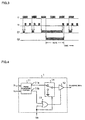
- Fig. 2 is a block diagram which illustrates the internal structure of the comparison signal presence/absence detector 5.
- 51, 52 are DFF circuits, and 53, 54 are inverters.
- a high level signal is inputted to the D terminal of the DFF circuit 51, and a test signal ft generated independently (and having a frequency less than or equal to 1/2 of the comparison signal fc and a duty ratio of 50%) is inputted to the CK terminal of the DFF circuit 51.
- the comparison signal fc is inputted to the R (reset) terminal of the DFF circuit 51 via the inverter 54.
- a signal from the Q1 terminal of the DFF circuit 51 is inputted to the D terminal of the DFF circuit 52, and the test signal ft is inverted at the inverter 53 and inputted to the CK terminal of the DFF circuit 52.
- Fig. 3 is a timing chart of operation of the comparison signal presence/absence detector 5.
- the Q1 terminal of the DFF circuit 51 senses a high level of the D terminal and becomes a high level.
- the comparison signal fc rises, the Q1 terminal of the DFF circuit 51 is reset and becomes a low level.
- the DFF circuit 52 outputs, to the Q2 terminal, data of the D terminal at the time the electric potential of the CK terminal rises.
- the comparison signal fc changes from H ⁇ L ⁇ H ⁇ ... at a predetermined period, even if the Q1 terminal of the DFF circuit 51 becomes a high level at the rise of the test signal ft, thereafter, the Q1 terminal of the DFF circuit 51 is reset at the rise of the comparison signal fc. Thus, thereafter, even if the test signal ft falls, the Q2 terminal of the DFF circuit 52 does not become a high level.
- the DFF circuit 51 when there is no comparison signal fc, in other words, when the comparison signal fc does not change to a high level, the DFF circuit 51 is not reset.
- the DFF circuit 52 senses the high level signal of the Q1 terminal and outputs it as a high level signal to the Q2 terminal, and thereafter continues this operation. Note that, thereafter, when the comparison signal fc starts to change again, the Q2 terminal of the DFF circuit 52 returns to a low level.
- Fig. 4 is a block diagram which illustrates the internal structure of the phase comparator 1 which is controlled by the signal detected at the comparison signal presence/absence detector 5.
- 11 is a phase comparing portion which is formed by an exclusive OR gate or the like
- 12 is a three state buffer
- 13 is an OR gate
- 14 is a switch circuit.
- the three state buffer 12, the OR gate 13 and the switch circuit 14 form a control means.
- the phase comparing portion 11 makes an output terminal 11a a low level.
- the phase comparing portion 11 makes the output terminal 11a a high level.
- the level is indefinite at times other than the times of phase comparison.
- a control terminal 11b of the phase comparing portion 11 is a high level, and at other times, is a low level.
- the OR gate 13 takes the logical sum of a control signal outputted from the control terminal 11b of the phase comparing portion 11 and a detection signal Va detected at the comparison signal presence/absence detector 5, and sends the logical sum to the control terminal of the buffer 12. Further, a signal of the output terminal 11a of the phase comparing portion 11 is inputted to the input side of the buffer 12 via the switch circuit 14. Moreover, the switch circuit 14 switches to the ground side (low level) when the detection signal Va becomes a high level.
- the buffer 12 is controlled according to the signal of the control terminal 11b of the phase comparing portion 11. Namely, during the time in which there is a phase offset between the comparison signal fc and the reference signal fr, the control terminal 11b is high level. Therefore, the buffer 12 is ON such that a signal can pass between the input and the output, and the signal of the output terminal 11a of the phase comparing portion 11 is outputted as it is via the switch circuit 14, and normal operation is carried out.
- the signal of the control terminal 11b When there is no phase offset (at times of PLL lock), the signal of the control terminal 11b is at a low level, and the output of the buffer 12 is high impedance. Due to the signal held at the loop filter 2 which is downstream of the phase comparator 1, thereafter, the voltage control oscillator 3 oscillates a constant frequency signal.
- the detection signal Va of the comparison signal presence/absence detector 5 is a signal-does-not-exist signal
- the detection signal Va when the detection signal Va is high level, the output of the switch circuit 14 is low level, and the buffer 12 turns ON such that a signal can pass between the input and the output. Therefore, the low level signal outputted from the switch circuit 14 is outputted as it is. Accordingly, the low level signal is inputted to the loop filter 2, and the control voltage Vc which is inputted to the voltage control oscillator 4 is low level, and the frequency oscillated thereat is low.
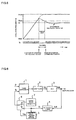
- Fig. 5 is a diagram which illustrates an operation characteristic of the voltage control oscillator 3.
- fo is a target frequency of the frequency signal fck
- fmax is an oscillation upper limit frequency
- fmin is a oscillation lower limit frequency
- flimit is an input frequency which is an operating limit of the frequency divider 4.
- the comparison signal fc disappears.
- the output signal of the phase comparator 1 is controlled to a low level
- the oscillation frequency of the voltage control oscillator 3 is controlled to a low frequency.
- the frequency divider 4 starts to operate again, and the PLL circuit returns to original operation, and the oscillation frequency fck settles to the target frequency fo.
- Fig. 6 is a block diagram which illustrates the structure of a PLL circuit of another embodiment.
- a switch circuit 6 is connected between the frequency divider 4 and the phase comparator 1.
- the switch circuit 6 is controlled such that the frequency divider 4 and the phase comparator 1 are connected to each other by the switch circuit 6.
- the switch circuit 6 is controlled so that a dummy pulse is inputted from a dummy pulse generator 7 as the comparison signal fc which is inputted to the phase comparator 1.
- the switch circuit 6 and the dummy pulse generator 7 form the control means.
- the dummy pulse may be a signal which is a higher frequency than a frequency of the frequency signal outputted from the frequency divider 4. In this way, in the present embodiment as well, when the voltage control oscillator 3 oscillates abnormally and the operation of the frequency divider 4 stops, operation can be returned to normal immediately.
- the output signal of the phase comparator 1 is forcibly made to be a special signal (low level signal) by the detection signal Va of the comparison signal presence/absence detector 5, or a special dummy pulse is inputted as the comparison signal to the phase comparator 1.
- the above-described embodiments are not limited to the same.
- the control voltage Vc of the voltage control oscillator 3 may be controlled directly by the detection signal Va of the comparison signal presence/absence detector 5 such that the oscillation frequency of the voltage control oscillator 3 is controlled to a specific low frequency. No special accuracy is demanded of this specific low frequency at this time.
- the operation stoppage state of the PLL circuit is judged by the presence/absence of an output signal of the frequency divider 4.
- the operation stoppage state of the PLL circuit may be judged by detecting by a separately provided voltage comparator whether or not the control voltage Va of the voltage control oscillator 3 is less than or equal to a predetermined level, or by detecting whether or not the oscillation frequency fck of the voltage control oscillator 3 is a frequency of a predetermined value or more.
- the signal of the frequency fck may be converted into a voltage signal by a frequency/voltage converter, and this voltage signal compared with a predetermined value by a voltage comparator.
- the present invention there is the advantage that, when an oscillation frequency of a voltage control oscillator exceeds a predetermined value and a PLL circuit stops operating, operation can return to normal quickly with a simple structure.
- the present invention is suitable for generation of a sampling clock of a wide range which is used when digitally processing analog image signals, and for the like.
Landscapes
- Stabilization Of Oscillater, Synchronisation, Frequency Synthesizers (AREA)
Abstract
Description
Claims (6)
- A PLL circuit in which a phase comparator, a loop filter, a voltage control oscillator and a frequency divider are successively loop-connected, said PLL circuit comprising:
operation stoppage detecting means for detecting that PLL operation has stopped; and control means for, when said operation, controlling the voltage control oscillator such that an oscillation frequency of the voltage control oscillator is low. - A PLL circuit according to claim 1, wherein said operation stoppage detecting means is a means for detecting presence/absence of an output signal of the frequency divider.
- A PLL circuit according to claim 1, wherein said operation stoppage detecting means is a means for detecting whether or not a control voltage of the voltage control oscillator is a value that oscillates a frequency which is greater than or equal to a predetermined value.
- A PLL circuit according to claim 1, wherein said operation stoppage detecting means is a means for detecting whether or not an oscillation frequency of the voltage control oscillator is value higher than a predetermined value.
- A PLL circuit according to any one of claims 1 through 4, wherein said control means is a means for switching an output of the phase comparator to a value at which an oscillation frequency of the voltage control oscillator decreases.
- A PLL circuit according to any one of claims 1 through 4, wherein said control means is a means for switching a comparison signal inputted to the phase comparator such that an oscillation frequency of the voltage control oscillator decreases.
Applications Claiming Priority (3)
| Application Number | Priority Date | Filing Date | Title |
|---|---|---|---|
| JP26716899 | 1999-09-21 | ||
| JP26716899A JP3849368B2 (en) | 1999-09-21 | 1999-09-21 | PLL circuit |
| PCT/JP2000/005629 WO2001022593A1 (en) | 1999-09-21 | 2000-08-23 | Phase-locked loop |
Publications (3)
| Publication Number | Publication Date |
|---|---|
| EP1143622A1 true EP1143622A1 (en) | 2001-10-10 |
| EP1143622A4 EP1143622A4 (en) | 2002-05-15 |
| EP1143622B1 EP1143622B1 (en) | 2003-10-15 |
Family
ID=17441057
Family Applications (1)
| Application Number | Title | Priority Date | Filing Date |
|---|---|---|---|
| EP00954915A Expired - Lifetime EP1143622B1 (en) | 1999-09-21 | 2000-08-23 | Phase-locked loop |
Country Status (13)
| Country | Link |
|---|---|
| US (1) | US6768357B1 (en) |
| EP (1) | EP1143622B1 (en) |
| JP (1) | JP3849368B2 (en) |
| KR (1) | KR100534196B1 (en) |
| CN (1) | CN1321360A (en) |
| AT (1) | ATE252292T1 (en) |
| AU (1) | AU771267B2 (en) |
| CA (1) | CA2351759C (en) |
| DE (1) | DE60005924T2 (en) |
| ES (1) | ES2204675T3 (en) |
| RU (1) | RU2235421C2 (en) |
| TW (1) | TW456107B (en) |
| WO (1) | WO2001022593A1 (en) |
Families Citing this family (7)
| Publication number | Priority date | Publication date | Assignee | Title |
|---|---|---|---|---|
| JP2002318265A (en) * | 2001-04-24 | 2002-10-31 | Hitachi Ltd | Semiconductor integrated circuit and method of testing semiconductor integrated circuit |
| US7085982B2 (en) * | 2002-01-18 | 2006-08-01 | Hitachi, Ltd. | Pulse generation circuit and semiconductor tester that uses the pulse generation circuit |
| JP2006254122A (en) * | 2005-03-10 | 2006-09-21 | Fujitsu Ltd | PLL circuit and method of controlling oscillation operation of PLL circuit |
| JP2007181046A (en) * | 2005-12-28 | 2007-07-12 | Matsushita Electric Ind Co Ltd | Receiving circuit, receiving apparatus and receiving method |
| KR100862509B1 (en) | 2007-03-09 | 2008-10-08 | 삼성전기주식회사 | Low Power Stack Structure Phase-Locked Loop |
| JP4667525B2 (en) * | 2007-06-22 | 2011-04-13 | 富士通セミコンダクター株式会社 | PLL control circuit, PLL device, and PLL control method |
| CN109379076A (en) * | 2018-10-24 | 2019-02-22 | 佛山市秀声电子科技有限公司 | A kind of low-frequency phase-locking ring that modulus combines |
Family Cites Families (15)
| Publication number | Priority date | Publication date | Assignee | Title |
|---|---|---|---|---|
| SU535715A1 (en) * | 1974-08-02 | 1976-11-15 | Северо-Западный Заочный Политехнический Институт | Device for phase locked loop |
| JPS51114058A (en) * | 1975-04-01 | 1976-10-07 | Nippon Gakki Seizo Kk | Pll system |
| US4461990A (en) * | 1982-10-01 | 1984-07-24 | General Electric Company | Phase control circuit for low voltage load |
| US4769704A (en) * | 1985-06-04 | 1988-09-06 | Matsushita Electric Industrial Co., Ltd. | Synchronization signal generator |
| JP2610171B2 (en) * | 1988-08-31 | 1997-05-14 | 日本電気エンジニアリング株式会社 | Phase locked loop |
| JP2710990B2 (en) * | 1989-07-12 | 1998-02-10 | 三菱電機株式会社 | Video intermediate frequency signal processing circuit |
| JPH04142812A (en) * | 1990-10-04 | 1992-05-15 | Toshiba Corp | Phase locked loop circuit |
| JPH06338786A (en) * | 1993-05-31 | 1994-12-06 | Sanyo Electric Co Ltd | Microcomputer |
| JP3395411B2 (en) * | 1994-11-21 | 2003-04-14 | ソニー株式会社 | Phase comparison circuit and phase synchronization circuit |
| US5598396A (en) * | 1995-02-15 | 1997-01-28 | Matsushita Electric Industrial Co., Ltd. | Optical disk reproducing apparatus |
| WO1997007594A1 (en) * | 1995-08-14 | 1997-02-27 | Hitachi, Ltd. | Pll circuit and picture reproducing device |
| DE19600722A1 (en) | 1996-01-11 | 1997-07-17 | Bayer Ag | Process for the preparation of optionally substituted 4-aminodiphenylamines |
| JPH10107627A (en) * | 1996-10-01 | 1998-04-24 | Kawasaki Steel Corp | PLL circuit |
| JPH11122102A (en) * | 1997-10-14 | 1999-04-30 | Kawasaki Steel Corp | PLL circuit |
| US5939949A (en) * | 1998-03-16 | 1999-08-17 | National Semiconductor Corporation | Self-adjusting startup control for charge pump current source in phase locked loop |
-
1999
- 1999-09-21 JP JP26716899A patent/JP3849368B2/en not_active Expired - Fee Related
-
2000
- 2000-07-29 TW TW089115257A patent/TW456107B/en not_active IP Right Cessation
- 2000-08-23 DE DE60005924T patent/DE60005924T2/en not_active Expired - Lifetime
- 2000-08-23 ES ES00954915T patent/ES2204675T3/en not_active Expired - Lifetime
- 2000-08-23 EP EP00954915A patent/EP1143622B1/en not_active Expired - Lifetime
- 2000-08-23 AT AT00954915T patent/ATE252292T1/en not_active IP Right Cessation
- 2000-08-23 US US09/806,054 patent/US6768357B1/en not_active Expired - Lifetime
- 2000-08-23 KR KR10-2001-7006351A patent/KR100534196B1/en not_active Expired - Fee Related
- 2000-08-23 AU AU67257/00A patent/AU771267B2/en not_active Ceased
- 2000-08-23 CA CA002351759A patent/CA2351759C/en not_active Expired - Fee Related
- 2000-08-23 CN CN00801804A patent/CN1321360A/en active Pending
- 2000-08-23 RU RU2001117072/09A patent/RU2235421C2/en not_active IP Right Cessation
- 2000-08-23 WO PCT/JP2000/005629 patent/WO2001022593A1/en not_active Ceased
Also Published As
| Publication number | Publication date |
|---|---|
| CN1321360A (en) | 2001-11-07 |
| CA2351759A1 (en) | 2001-03-29 |
| US6768357B1 (en) | 2004-07-27 |
| KR20010093790A (en) | 2001-10-29 |
| DE60005924D1 (en) | 2003-11-20 |
| AU771267B2 (en) | 2004-03-18 |
| TW456107B (en) | 2001-09-21 |
| KR100534196B1 (en) | 2005-12-08 |
| EP1143622B1 (en) | 2003-10-15 |
| EP1143622A4 (en) | 2002-05-15 |
| ATE252292T1 (en) | 2003-11-15 |
| AU6725700A (en) | 2001-04-24 |
| JP3849368B2 (en) | 2006-11-22 |
| JP2001094416A (en) | 2001-04-06 |
| ES2204675T3 (en) | 2004-05-01 |
| DE60005924T2 (en) | 2004-05-06 |
| RU2235421C2 (en) | 2004-08-27 |
| WO2001022593A1 (en) | 2001-03-29 |
| CA2351759C (en) | 2004-03-09 |
Similar Documents
| Publication | Publication Date | Title |
|---|---|---|
| US7622996B2 (en) | Multi-loop phase locked loop circuit | |
| US6483361B1 (en) | Lock detector for determining phase lock condition in PLL on a period-by-period basis according to desired phase error | |
| US7558311B2 (en) | Spread spectrum clock generator and method for generating a spread spectrum clock signal | |
| US7321649B2 (en) | Phase locked loop with improved phase lock/unlock detection function | |
| US12401367B2 (en) | PLL circuit and transmission system | |
| US20100156482A1 (en) | Means to detect a missing pulse and reduce the associated pll phase bump | |
| US7663417B2 (en) | Phase-locked loop circuit | |
| EP0094837A2 (en) | Phase-locked circuit loop having improved locking capabilities | |
| EP0798861A1 (en) | Phase synchronization system | |
| US6792064B2 (en) | Multiple phase-locked loop circuit | |
| EP1143622B1 (en) | Phase-locked loop | |
| US6518845B2 (en) | PLL frequency synthesizer circuit | |
| US6757349B1 (en) | PLL frequency synthesizer with lock detection circuit | |
| US6965660B2 (en) | Digital phase-locked loop | |
| US20030214330A1 (en) | Phase-locked loop circuit | |
| JP3356715B2 (en) | PLL circuit | |
| US20020021368A1 (en) | PLL circuit for CRT monitor horizontal drive signal | |
| US6559725B1 (en) | Phase noise reduction system for frequency synthesizer and method thereof | |
| JPH08172355A (en) | PLL circuit | |
| JPH10233681A (en) | PLL circuit | |
| US7355487B2 (en) | Method for reducing phase lock time and jittering and phase lock loop using the same | |
| JP2000022529A (en) | Phase locked loop | |
| JPH07326969A (en) | Pll circuit | |
| JP2000078003A (en) | PLL circuit | |
| JP2003152532A (en) | Phase locked loop circuit |
Legal Events
| Date | Code | Title | Description |
|---|---|---|---|
| PUAI | Public reference made under article 153(3) epc to a published international application that has entered the european phase |
Free format text: ORIGINAL CODE: 0009012 |
|
| 17P | Request for examination filed |
Effective date: 20010305 |
|
| AK | Designated contracting states |
Kind code of ref document: A1 Designated state(s): AT BE CH CY DE DK ES FI FR GB GR IE IT LI LU MC NL PT SE |
|
| A4 | Supplementary search report drawn up and despatched |
Effective date: 20020328 |
|
| AK | Designated contracting states |
Kind code of ref document: A4 Designated state(s): AT BE CH CY DE DK ES FI FR GB GR IE IT LI LU MC NL PT SE |
|
| RIC1 | Information provided on ipc code assigned before grant |
Free format text: 7H 03L 7/083 A, 7H 03L 7/10 B |
|
| 17Q | First examination report despatched |
Effective date: 20020913 |
|
| GRAH | Despatch of communication of intention to grant a patent |
Free format text: ORIGINAL CODE: EPIDOS IGRA |
|
| GRAS | Grant fee paid |
Free format text: ORIGINAL CODE: EPIDOSNIGR3 |
|
| GRAA | (expected) grant |
Free format text: ORIGINAL CODE: 0009210 |
|
| AK | Designated contracting states |
Kind code of ref document: B1 Designated state(s): AT BE CH CY DE DK ES FI FR GB GR IE IT LI LU MC NL PT SE |
|
| PG25 | Lapsed in a contracting state [announced via postgrant information from national office to epo] |
Ref country code: CH Free format text: LAPSE BECAUSE OF FAILURE TO SUBMIT A TRANSLATION OF THE DESCRIPTION OR TO PAY THE FEE WITHIN THE PRESCRIBED TIME-LIMIT Effective date: 20031015 Ref country code: CY Free format text: LAPSE BECAUSE OF FAILURE TO SUBMIT A TRANSLATION OF THE DESCRIPTION OR TO PAY THE FEE WITHIN THE PRESCRIBED TIME-LIMIT Effective date: 20031015 Ref country code: FI Free format text: LAPSE BECAUSE OF FAILURE TO SUBMIT A TRANSLATION OF THE DESCRIPTION OR TO PAY THE FEE WITHIN THE PRESCRIBED TIME-LIMIT Effective date: 20031015 Ref country code: LI Free format text: LAPSE BECAUSE OF FAILURE TO SUBMIT A TRANSLATION OF THE DESCRIPTION OR TO PAY THE FEE WITHIN THE PRESCRIBED TIME-LIMIT Effective date: 20031015 Ref country code: BE Free format text: LAPSE BECAUSE OF FAILURE TO SUBMIT A TRANSLATION OF THE DESCRIPTION OR TO PAY THE FEE WITHIN THE PRESCRIBED TIME-LIMIT Effective date: 20031015 Ref country code: AT Free format text: LAPSE BECAUSE OF FAILURE TO SUBMIT A TRANSLATION OF THE DESCRIPTION OR TO PAY THE FEE WITHIN THE PRESCRIBED TIME-LIMIT Effective date: 20031015 |
|
| REG | Reference to a national code |
Ref country code: GB Ref legal event code: FG4D Ref country code: CH Ref legal event code: EP |
|
| REG | Reference to a national code |
Ref country code: IE Ref legal event code: FG4D |
|
| REF | Corresponds to: |
Ref document number: 60005924 Country of ref document: DE Date of ref document: 20031120 Kind code of ref document: P |
|
| PG25 | Lapsed in a contracting state [announced via postgrant information from national office to epo] |
Ref country code: GR Free format text: LAPSE BECAUSE OF FAILURE TO SUBMIT A TRANSLATION OF THE DESCRIPTION OR TO PAY THE FEE WITHIN THE PRESCRIBED TIME-LIMIT Effective date: 20040115 Ref country code: DK Free format text: LAPSE BECAUSE OF FAILURE TO SUBMIT A TRANSLATION OF THE DESCRIPTION OR TO PAY THE FEE WITHIN THE PRESCRIBED TIME-LIMIT Effective date: 20040115 Ref country code: SE Free format text: LAPSE BECAUSE OF FAILURE TO SUBMIT A TRANSLATION OF THE DESCRIPTION OR TO PAY THE FEE WITHIN THE PRESCRIBED TIME-LIMIT Effective date: 20040115 |
|
| REG | Reference to a national code |
Ref country code: CH Ref legal event code: PL |
|
| REG | Reference to a national code |
Ref country code: ES Ref legal event code: FG2A Ref document number: 2204675 Country of ref document: ES Kind code of ref document: T3 |
|
| ET | Fr: translation filed | ||
| PLBE | No opposition filed within time limit |
Free format text: ORIGINAL CODE: 0009261 |
|
| STAA | Information on the status of an ep patent application or granted ep patent |
Free format text: STATUS: NO OPPOSITION FILED WITHIN TIME LIMIT |
|
| PG25 | Lapsed in a contracting state [announced via postgrant information from national office to epo] |
Ref country code: LU Free format text: LAPSE BECAUSE OF NON-PAYMENT OF DUE FEES Effective date: 20040823 Ref country code: IE Free format text: LAPSE BECAUSE OF NON-PAYMENT OF DUE FEES Effective date: 20040823 |
|
| PG25 | Lapsed in a contracting state [announced via postgrant information from national office to epo] |
Ref country code: MC Free format text: LAPSE BECAUSE OF NON-PAYMENT OF DUE FEES Effective date: 20040831 |
|
| 26N | No opposition filed |
Effective date: 20040716 |
|
| REG | Reference to a national code |
Ref country code: IE Ref legal event code: MM4A |
|
| PG25 | Lapsed in a contracting state [announced via postgrant information from national office to epo] |
Ref country code: PT Free format text: LAPSE BECAUSE OF NON-PAYMENT OF DUE FEES Effective date: 20040315 |
|
| REG | Reference to a national code |
Ref country code: GB Ref legal event code: 732E |
|
| NLS | Nl: assignments of ep-patents |
Owner name: CANON INC. Effective date: 20080731 |
|
| PGFP | Annual fee paid to national office [announced via postgrant information from national office to epo] |
Ref country code: ES Payment date: 20080922 Year of fee payment: 9 Ref country code: NL Payment date: 20080803 Year of fee payment: 9 |
|
| PGFP | Annual fee paid to national office [announced via postgrant information from national office to epo] |
Ref country code: FR Payment date: 20080818 Year of fee payment: 9 Ref country code: IT Payment date: 20080828 Year of fee payment: 9 |
|
| REG | Reference to a national code |
Ref country code: FR Ref legal event code: TP |
|
| REG | Reference to a national code |
Ref country code: ES Ref legal event code: PC2A |
|
| REG | Reference to a national code |
Ref country code: NL Ref legal event code: V1 Effective date: 20100301 |
|
| REG | Reference to a national code |
Ref country code: FR Ref legal event code: ST Effective date: 20100430 |
|
| PG25 | Lapsed in a contracting state [announced via postgrant information from national office to epo] |
Ref country code: NL Free format text: LAPSE BECAUSE OF NON-PAYMENT OF DUE FEES Effective date: 20100301 Ref country code: FR Free format text: LAPSE BECAUSE OF NON-PAYMENT OF DUE FEES Effective date: 20090831 |
|
| REG | Reference to a national code |
Ref country code: ES Ref legal event code: FD2A Effective date: 20090824 |
|
| PG25 | Lapsed in a contracting state [announced via postgrant information from national office to epo] |
Ref country code: IT Free format text: LAPSE BECAUSE OF NON-PAYMENT OF DUE FEES Effective date: 20090823 |
|
| PG25 | Lapsed in a contracting state [announced via postgrant information from national office to epo] |
Ref country code: ES Free format text: LAPSE BECAUSE OF NON-PAYMENT OF DUE FEES Effective date: 20090824 |
|
| PGFP | Annual fee paid to national office [announced via postgrant information from national office to epo] |
Ref country code: DE Payment date: 20130831 Year of fee payment: 14 |
|
| PGFP | Annual fee paid to national office [announced via postgrant information from national office to epo] |
Ref country code: GB Payment date: 20130822 Year of fee payment: 14 |
|
| REG | Reference to a national code |
Ref country code: DE Ref legal event code: R119 Ref document number: 60005924 Country of ref document: DE |
|
| GBPC | Gb: european patent ceased through non-payment of renewal fee |
Effective date: 20140823 |
|
| REG | Reference to a national code |
Ref country code: DE Ref legal event code: R119 Ref document number: 60005924 Country of ref document: DE Effective date: 20150303 |
|
| PG25 | Lapsed in a contracting state [announced via postgrant information from national office to epo] |
Ref country code: GB Free format text: LAPSE BECAUSE OF NON-PAYMENT OF DUE FEES Effective date: 20140823 Ref country code: DE Free format text: LAPSE BECAUSE OF NON-PAYMENT OF DUE FEES Effective date: 20150303 |