EP1143518A1 - Resin-molded unit including an electronic circuit component covered by a protective magnetic film - Google Patents
Resin-molded unit including an electronic circuit component covered by a protective magnetic film Download PDFInfo
- Publication number
- EP1143518A1 EP1143518A1 EP01108513A EP01108513A EP1143518A1 EP 1143518 A1 EP1143518 A1 EP 1143518A1 EP 01108513 A EP01108513 A EP 01108513A EP 01108513 A EP01108513 A EP 01108513A EP 1143518 A1 EP1143518 A1 EP 1143518A1
- Authority
- EP
- European Patent Office
- Prior art keywords
- resin
- magnetic
- frequency
- molded unit
- electronic circuit
- Prior art date
- Legal status (The legal status is an assumption and is not a legal conclusion. Google has not performed a legal analysis and makes no representation as to the accuracy of the status listed.)
- Withdrawn
Links
Images



Classifications
-
- H—ELECTRICITY
- H10—SEMICONDUCTOR DEVICES; ELECTRIC SOLID-STATE DEVICES NOT OTHERWISE PROVIDED FOR
- H10W—GENERIC PACKAGES, INTERCONNECTIONS, CONNECTORS OR OTHER CONSTRUCTIONAL DETAILS OF DEVICES COVERED BY CLASS H10
- H10W74/00—Encapsulations, e.g. protective coatings
- H10W74/01—Manufacture or treatment
-
- H—ELECTRICITY
- H10—SEMICONDUCTOR DEVICES; ELECTRIC SOLID-STATE DEVICES NOT OTHERWISE PROVIDED FOR
- H10W—GENERIC PACKAGES, INTERCONNECTIONS, CONNECTORS OR OTHER CONSTRUCTIONAL DETAILS OF DEVICES COVERED BY CLASS H10
- H10W74/00—Encapsulations, e.g. protective coatings
- H10W74/10—Encapsulations, e.g. protective coatings characterised by their shape or disposition
- H10W74/111—Encapsulations, e.g. protective coatings characterised by their shape or disposition the semiconductor body being completely enclosed
- H10W74/121—Encapsulations, e.g. protective coatings characterised by their shape or disposition the semiconductor body being completely enclosed by multiple encapsulations, e.g. by a thin protective coating and a thick encapsulation
-
- H—ELECTRICITY
- H10—SEMICONDUCTOR DEVICES; ELECTRIC SOLID-STATE DEVICES NOT OTHERWISE PROVIDED FOR
- H10W—GENERIC PACKAGES, INTERCONNECTIONS, CONNECTORS OR OTHER CONSTRUCTIONAL DETAILS OF DEVICES COVERED BY CLASS H10
- H10W42/00—Arrangements for protection of devices
-
- H—ELECTRICITY
- H10—SEMICONDUCTOR DEVICES; ELECTRIC SOLID-STATE DEVICES NOT OTHERWISE PROVIDED FOR
- H10W—GENERIC PACKAGES, INTERCONNECTIONS, CONNECTORS OR OTHER CONSTRUCTIONAL DETAILS OF DEVICES COVERED BY CLASS H10
- H10W42/00—Arrangements for protection of devices
- H10W42/20—Arrangements for protection of devices protecting against electromagnetic or particle radiation, e.g. light, X-rays, gamma-rays or electrons
-
- H—ELECTRICITY
- H10—SEMICONDUCTOR DEVICES; ELECTRIC SOLID-STATE DEVICES NOT OTHERWISE PROVIDED FOR
- H10W—GENERIC PACKAGES, INTERCONNECTIONS, CONNECTORS OR OTHER CONSTRUCTIONAL DETAILS OF DEVICES COVERED BY CLASS H10
- H10W42/00—Arrangements for protection of devices
- H10W42/20—Arrangements for protection of devices protecting against electromagnetic or particle radiation, e.g. light, X-rays, gamma-rays or electrons
- H10W42/261—Arrangements for protection of devices protecting against electromagnetic or particle radiation, e.g. light, X-rays, gamma-rays or electrons characterised by their shapes or dispositions
- H10W42/276—Arrangements for protection of devices protecting against electromagnetic or particle radiation, e.g. light, X-rays, gamma-rays or electrons characterised by their shapes or dispositions the arrangements being on an external surface of the package, e.g. on the outer surface of an encapsulation
-
- H—ELECTRICITY
- H10—SEMICONDUCTOR DEVICES; ELECTRIC SOLID-STATE DEVICES NOT OTHERWISE PROVIDED FOR
- H10W—GENERIC PACKAGES, INTERCONNECTIONS, CONNECTORS OR OTHER CONSTRUCTIONAL DETAILS OF DEVICES COVERED BY CLASS H10
- H10W42/00—Arrangements for protection of devices
- H10W42/20—Arrangements for protection of devices protecting against electromagnetic or particle radiation, e.g. light, X-rays, gamma-rays or electrons
- H10W42/281—Arrangements for protection of devices protecting against electromagnetic or particle radiation, e.g. light, X-rays, gamma-rays or electrons characterised by their materials
- H10W42/287—Arrangements for protection of devices protecting against electromagnetic or particle radiation, e.g. light, X-rays, gamma-rays or electrons characterised by their materials materials for magnetic shielding, e.g. ferromagnetic materials
-
- H—ELECTRICITY
- H10—SEMICONDUCTOR DEVICES; ELECTRIC SOLID-STATE DEVICES NOT OTHERWISE PROVIDED FOR
- H10W—GENERIC PACKAGES, INTERCONNECTIONS, CONNECTORS OR OTHER CONSTRUCTIONAL DETAILS OF DEVICES COVERED BY CLASS H10
- H10W44/00—Electrical arrangements for controlling or matching impedance
- H10W44/20—Electrical arrangements for controlling or matching impedance at high-frequency [HF] or radio frequency [RF]
-
- H—ELECTRICITY
- H10—SEMICONDUCTOR DEVICES; ELECTRIC SOLID-STATE DEVICES NOT OTHERWISE PROVIDED FOR
- H10W—GENERIC PACKAGES, INTERCONNECTIONS, CONNECTORS OR OTHER CONSTRUCTIONAL DETAILS OF DEVICES COVERED BY CLASS H10
- H10W72/00—Interconnections or connectors in packages
- H10W72/071—Connecting or disconnecting
- H10W72/075—Connecting or disconnecting of bond wires
-
- H—ELECTRICITY
- H10—SEMICONDUCTOR DEVICES; ELECTRIC SOLID-STATE DEVICES NOT OTHERWISE PROVIDED FOR
- H10W—GENERIC PACKAGES, INTERCONNECTIONS, CONNECTORS OR OTHER CONSTRUCTIONAL DETAILS OF DEVICES COVERED BY CLASS H10
- H10W72/00—Interconnections or connectors in packages
- H10W72/90—Bond pads, in general
- H10W72/951—Materials of bond pads
-
- H—ELECTRICITY
- H10—SEMICONDUCTOR DEVICES; ELECTRIC SOLID-STATE DEVICES NOT OTHERWISE PROVIDED FOR
- H10W—GENERIC PACKAGES, INTERCONNECTIONS, CONNECTORS OR OTHER CONSTRUCTIONAL DETAILS OF DEVICES COVERED BY CLASS H10
- H10W74/00—Encapsulations, e.g. protective coatings
-
- H—ELECTRICITY
- H10—SEMICONDUCTOR DEVICES; ELECTRIC SOLID-STATE DEVICES NOT OTHERWISE PROVIDED FOR
- H10W—GENERIC PACKAGES, INTERCONNECTIONS, CONNECTORS OR OTHER CONSTRUCTIONAL DETAILS OF DEVICES COVERED BY CLASS H10
- H10W90/00—Package configurations
- H10W90/701—Package configurations characterised by the relative positions of pads or connectors relative to package parts
- H10W90/751—Package configurations characterised by the relative positions of pads or connectors relative to package parts of bond wires
- H10W90/756—Package configurations characterised by the relative positions of pads or connectors relative to package parts of bond wires between a chip and a stacked lead frame, conducting package substrate or heat sink
Definitions
- This invention relates to a resin-molded unit comprising an electronic circuit component, such as a semiconductor chip, sealed in a resin mold.
- an electronic circuit component such as a semiconductor chip
- resin mold a resin-molded unit
- the term "resin-molded unit” is used in a broad sense including a resin case and a resin housing also.
- RAM random access memory
- ROM read only memory
- MPU microprocessor
- CPU central processing unit
- IPALU image processor arithmetic logic unit
- a resin-molded unit comprising an electronic circuit component, such as a semiconductor chip, sealed in a resin mold. It is pointed out that such resin-molded unit has a problem of undesired radiation produced from a power supply line. In order to avoid the problem, various countermeasures have been taken. For example, a lumped constant component such as a decoupling capacitor is inserted into the power supply line.
- the noise generated as mentioned above will contain a harmonic component.
- a signal path exhibits the behavior as a distributed constant circuit. Therefore, the conventional technique of preventing the noise is not effective because such technique assumes a lumped constant circuit.
- a resin-molded unit comprising an electronic circuit component, a resin molding the electronic circuit component therein, and a high-frequency current suppressor covering at least one part of the resin, the high-frequency current suppressor being made of a magnetic loss film.
- a resin-molded unit comprising an electronic circuit component, a resin molding the electronic circuit component therein, and a high-frequency current suppressor covering at least one part of the resin, the high-frequency current suppressor being made of a magnetic loss film which serves to attenuate a high-frequency current flowing through the electronic circuit component and having a frequency within a frequency band between several tens MHz and several GHz.
- a resin-molded unit comprising an electronic circuit component, a resin molding the electronic circuit component therein, and a high-frequency current suppressor covering at least one part of the resin, the high-frequency current suppressor being made of a magnetic loss film which is made of a magnetic substance of a magnetic composition comprising M, X and Y, where M is a metallic magnetic material consisting of Fe, Co, and/or Ni, X being element or elements other than M and Y, and Y being F, N, and/or O, the M-X-Y magnetic composition having a concentration of M in the composition so that the M-X-Y magnetic composition has a saturation magnetization of 35-80% of that of the metallic bulk of magnetic material comprising M alone, the magnetic composition having the maximum value ⁇ " max of an imaginary part ⁇ " of relative permeability in a frequency range of 0.1-10 gigahertz (GHz).
- M is a metallic magnetic material consisting of Fe, Co, and/or Ni
- X being element or elements other than M and Y
- Y
- the resin-molded unit is depicted by a reference numeral 1 and contains a semiconductor bear chip 2 arranged inside and sealed in an epoxy resin mold 3. From the semiconductor bear chip 2, a plurality of lead frames 4 are extracted through the epoxy resin mold 3 to the outside.
- the epoxy resin mold 3 is entirely covered with a high-frequency current suppressor 5.
- the high-frequency current suppressor 5 is a thin film magnetic substance formed in the form of a film by sputtering or vapor deposition known in the art, having a thickness between 0.3 ⁇ m and 20 ⁇ m, and exhibiting the conductivity in a frequency band lower than several tens MHz.
- the high-frequency current suppressor 5 serves to attenuate a high-frequency current flowing through a circuit portion inside the epoxy resin mold 3 and having a frequency within a frequency band between several tens MHz and several GHz.
- CVD chemical vapor deposition
- ion beam deposition ion beam deposition
- gas deposition ion beam deposition
- pattern transfer in addition to the sputtering or the vapor deposition mentioned above.
- a narrow-band magnetic loss material which has an M-X-Y composition as a mixture of components or elements M (M being at least one of Fe, Co, and Ni), Y (Y being at least one of F, N, and O), and X (X being at least one element other than those contained in M and Y) and which has a permeability characteristic, given as a relationship between a frequency and an imaginary part ⁇ " with respect to a real part ⁇ ' of relative permeability, such that the maximum value ⁇ " max of the imaginary part ⁇ " (which may be called a magnetic loss term) is present within a frequency range between 100MHz and 10GHz and that a relative bandwidth bwr is not greater than 200% where the relative bandwidth bwr is obtained by extracting a frequency bandwidth between two frequencies at which the value of ⁇ " is 50% of the maximum ⁇ " max and normalizing the frequency bandwidth at the center frequency thereof.
- M being at least one of Fe, Co, and Ni
- Y being at least one of F, N, and O
- the narrow-band magnetic loss material has saturation magnetization between 80% and 60% of that of a metal magnetic material comprising the component M alone and a d.c. electric resistance between 100 ⁇ ⁇ ⁇ cm and 700 ⁇ ⁇ ⁇ cm.
- a wide-band magnetic loss material which has an M-X-Y composition as a mixture of components M (M being at least one of Fe, Co, and Ni), Y (Y being at least one of F, N, and O), and X (X being at least one element other than those contained in M and Y) and which has a permeability characteristic, given as a relationship between a frequency and an imaginary part ⁇ " with respect to a real part ⁇ ' of relative permeability, such that the maximum value ⁇ " max of the imaginary part ⁇ " is present within a frequency range between 100MHz and 10GHz and that a relative bandwidth bwr is not smaller than 150% where the relative bandwidth bwr is obtained by extracting a frequency bandwidth between two frequencies at which the value of ⁇ " is 50% of the maximum ⁇ " max and normalizing the frequency bandwidth at the center frequency thereof. It is assumed here that the wide-band magnetic loss material has saturation magnetization between M (M being at least one of Fe, Co, and Ni), Y (Y being at least one of F, N
- the component X is at least one of C, B, Si, Al, Mg, Ti, Zn, Hf, Sr, Nb, Ta, and rare earth elements.
- the component M is present in a granular structure where particles or grains of the component M are dispersed in a matrix of a compound of the components X and Y. The particles have an average particle size between 1 nm and 40nm.
- the narrow-band or the wide-band magnetic loss material has an anisotropic magnetic field of 47400 A/m or less.
- the M-X-Y composition of the wide-band or the narrow-band magnetic loss material is an Fe-Al-O composition or an Fe-Si-O composition.
- the resin-molded unit 1 is similar in appearance to that of the conventional product but is superior in effect. Specifically, even in occurrence of a harmonic current as an undesired harmonic having a frequency ranging from several tens MHz to several GHz, such high-frequency can be sufficiently attenuated by the high-frequency current suppressor 5. As a result, production of a high-frequency noise can be prevented so as to remove an adverse affect by the high-frequency noise.
- the high-frequency current suppressor 5 use is made of a thin-film magnetic substance which is small in volume and therefore requires less space and which is a magnetic loss material having a large imaginary part (i.e., a "magnetic loss term") ⁇ " of relative permeability so as to provide effective protection against undesired radiation.
- a magnetic substance which shows large magnetic loss a granular magnetic material is known. Specifically, in case where the concentration of magnetic metal particles in the granular magnetic material falls within a particular range, excellent magnetic loss characteristic can be obtained in a high-frequency region.
- particles 11 of metallic magnetic material M are uniformly or evenly distributed in a matrix 12 consisting of X and Y.
- the sputtering apparatus has a conventional structure and comprises a vacuum container 20, a shutter 21, an atmospheric gas source 22, a substrate or a glass plate 23, chips 24 (X or X-Y), a target 25 (M), an RF power source, and a vacuum pump 27.
- the atmospheric gas source 22 and the vacuum pump 27 are connected to the vacuum container 20.
- the substrate 23 confronts to the target 25 on which chips 24 are disposed.
- the shutter 21 is disposed in front of the substrate 21.
- the RF power source 26 is connected to the target 25.
- a vapor deposition apparatus shown therein was also used another apparatus for producing samples in the following examples and comparative examples.
- the vapor deposition apparatus has a conventional structure and has vacuum container 20, atmospheric gas source 22, and vacuum pump 27 similar to the sputtering apparatus but has a crucible 28 including materials (X-Y) in place of chips 24, target 25 and RF power source 26.
- a thin film of M-X-Y magnetic composition was made on a glass plate by use of the sputtering apparatus shown in Fig. 3A at a sputtering condition shown in Table 1.
- Vacuum degree before sputtering ⁇ 1 ⁇ 10 -6 Torr Atmosphere Ar gas Electric Power RF Targets Fe (diameter of 100mm) and Al 2 O 3 chip (120 pieces) (chip size: 5mm ⁇ 5mm ⁇ 2mm)
- the film sample 1 produced was analyzed by a fluorescent X-ray spectroscopy and confirmed as a film of a composition Fe 72 Al 11 O 17 .
- the film sample 1 had 2.0 micrometer ( ⁇ m) in thickness, 530 micro ohm centimeters ( ⁇ ⁇ • cm) in DC specific resistance, 18 Oe in anisotropy field (Hk), and 16,800 Gauss in saturation magnetization (Ms).
- a percent ratio of the saturation magnetization of the film sample 1 and that of the metallic material M itself ⁇ Ms(M-X-Y)/Ms(M) ⁇ 100 was 72.2%.
- the film sample 1 was formed in a ribbon like form and inserted in a coil. Under application of a bias magnetic field, an impedance variation of the coil was measured in response to frequency change of AC current applied to the coil. The measurement was several times for different values of the bias magnetic field. From the measured impedance variation in response to frequency variation, the permeability frequency response ( ⁇ "-f response) was calculated and is shown in Fig. 4. It will be noted from Fig. 4 that the imaginary part of relative permeability has a high peak or the maximum value ( ⁇ " max ) and rapidly falls either side of the peak. The natural resonance frequency (f( ⁇ " max )) showing the maximum value ( ⁇ " max ) is about 700 MHz.
- a relative bandwidth bwr was determined as a percentage ratio of bandwidth between two frequency points which shows the imaginary part of relative permeability as a half value ⁇ " 50 of the maximum value ⁇ " max , to center frequency of said bandwidth.
- the relative bandwidth bwr was 148%.
- Example 2 In a condition similar to that in Example 1 but using of 150 Al 2 O 3 chips, a film sample 2 was formed on a glass plate.
- the film sample 2 produced was analyzed by a fluorescent X-ray spectroscopy and confirmed as a film of a composition Fe 44 Al 22 O 34 .
- the film sample 2 had 1.2 micrometer ( ⁇ m) in thickness, 2400 micro ohm centimeters ( ⁇ ⁇ ⁇ cm) in DC specific resistance, 120 Oe in anisotropy field (Hk), and 9600 Gauss in saturation magnetization (Ms). It will be noted that film sample 2 is higher than film sample 1 in the specific resistance.
- a percent ratio of the saturation magnetization of the film sample 2 and that of the metallic material M itself ⁇ Ms(M-X-Y)/Ms(M) ⁇ 100 was 44.5%.
- the ⁇ "-f response of film sample 2 was also obtained in the similar manner as in Example 1 and shows in Fig. 5. It is noted that the peak has also a high value similar to that in film sample 1. However, the frequency point at the peak, or the natural resonance frequency is about 1 GHz and the imaginary part of relative permeability gradually falls either side of the peak so that the ⁇ "-f response has a broadband characteristic.
- a relative bandwidth bwr of film sample 2 was also confirmed as 181% by the similar way as in Example 1.
- Example 1 In a condition similar to that in Example 1 but using of 90 Al 2 O 3 chips, a comparative sample 1 was formed on a glass plate.
- the comparative sample 1 produced was analyzed by a fluorescent X-ray spectroscopy and confirmed as a film of a composition Fe 86 Al 6 O 8 .
- the comparative sample 1 had 1.2 micrometer ( ⁇ m) in thickness, 74 micro ohm centimeters ( ⁇ ⁇ • cm) in DC specific resistance, 22 Oe in anisotropy field (Hk), 18,800 Gauss in saturation magnetization (Ms), and 85.7% in a percent ratio of the saturation magnetization of the comparative sample 1 and that of the metallic material M itself ⁇ Ms(M-X-Y)/Ms(M) ⁇ 100, and. was 44.5%.
- the ⁇ "-f response of comparative sample 1 was also obtained in the similar manner as in Example 1, and is shown in Fig. 6. It will be noted from Fig. 6 that the imaginary part ⁇ " of relative permeability of the comparative sample 1 has a high peak at a frequency about 10 MHz but rapidly reduces at the higher frequency range than 10 MHz. It can be supposed that this reduction is caused by generation of eddy current due to the lower specific resistance.
- a comparative sample 2 was formed on a glass plate.
- the comparative sample 2 produced was analyzed by a fluorescent X-ray spectroscopy and confirmed as a film of a composition Fe 19 Al 34 O 47 .
- the comparative sample 2 had 1.3 micrometer ( ⁇ m) in thickness, 10,500 micro ohm centimeters ( ⁇ ⁇ • cm) in DC specific resistance.
- the magnetic characteristic of comparative sample 1 exhibited superparamagnetism.
- a thin film of M-X-Y magnetic composition was made on a glass plate by the reactive sputtering method using the sputtering apparatus shown in Fig. 3A at a sputtering condition shown in Table 2.
- the partial pressure ratio of N 2 was 20%.
- the thin film was heat-treated at a temperature of 300°C for two hours in vacuum under magnetic field and obtained a film sample 4.
- Vacuum degree before sputtering ⁇ 1 ⁇ 10 -6 Torr Atmosphere Ar+N 2 gas Electric Power RF Targets Fe (diameter of 100mm) and Al chip (150 pieces) (chip size: 5mm ⁇ 5mm ⁇ 2mm)
- film sample 4 The properties of film sample 4 are show in Table 3. Film thickness 1.5 ⁇ m ⁇ Ms(M-X-Y)/Ms(M) ⁇ 100 51.9% ⁇ " max 520 f( ⁇ " max ) 830MHz bwr 175%
- a thin film of M-X-Y magnetic composition was made on a glass plate by using the sputtering apparatus shown in Fig. 3A at a sputtering condition shown in Table 4.
- the thin film was heat-treated at a temperature of 300°C for two hours in vacuum under magnetic field and obtained a film sample 5.
- Vacuum degree before sputtering ⁇ 1 ⁇ 10 -6 Torr Atmosphere Ar gas Electric Power RF Targets Co (diameter of 100mm) and Al 2 O 3 chip (130 pieces) (chip size: 5mm ⁇ 5mm ⁇ 2mm)
- film sample 5 The properties of film sample 5 are show in Table 5. Film thickness 1.1 ⁇ m ⁇ Ms(M-X-Y)/Ms(M) ⁇ 100 64.7% ⁇ " max 850 f( ⁇ " max ) 800MHz bwr 157%
- a thin film of M-X-Y magnetic composition was made on a glass plate by the reactive sputtering method using the sputtering apparatus shown in Fig. 3A at a sputtering condition shown in Table 6.
- the partial pressure ratio of N 2 was 10%.
- the thin film was heat-treated at a temperature of 300°C for two hours in vacuum under magnetic field and obtained a film sample 6. Vacuum degree before sputtering ⁇ 1 ⁇ 10 -6 Torr Atmosphere Ar+N 2 gas Electric Power RF Targets Co (diameter of 100mm) and Al chip (170 pieces) (chip size: 5mm ⁇ 5mm ⁇ 2mm)
- film sample 6 The properties of film sample 6 are show in Table 7. Film thickness 1.2 ⁇ m ⁇ Ms(M-X-Y)/Ms(M) ⁇ 100 32.7% ⁇ " max 350 f( ⁇ " max ) 1GHz bwr 191%
- a thin film of M-X-Y magnetic composition was made on a glass plate by using the sputtering apparatus shown in Fig. 3A at a sputtering condition shown in Table 8.
- the thin film was heat-treated at a temperature of 300°C for two hours in vacuum under magnetic field and obtained a film sample 7.
- film sample 4 The properties of film sample 4 are show in Table 9. Film thickness 1.7 ⁇ m ⁇ Ms(M-X-Y)/Ms(M) ⁇ 100 58.2% ⁇ " max 280 f( ⁇ " max ) 240MHz bwr 169%
- a thin film of M-X-Y magnetic composition was made on a glass plate by the reactive sputtering method using the sputtering apparatus shown in Fig. 3A at a sputtering condition shown in Table 10.
- the partial pressure ratio of N 2 was 10%.
- the thin film was heat-treated at a temperature of 300°C for two hours in vacuum under magnetic field and obtained a film sample 8.
- film sample 10 The properties of film sample 10 are show in Table 11. Film thickness 1.3 ⁇ m ⁇ Ms(M-X-Y)/Ms(M) ⁇ 100 76.2% ⁇ " max 410 f( ⁇ " max ) 170MHz bwr 158%
- a thin film of M-X-Y magnetic composition was made on a glass plate by using the sputtering apparatus shown in Fig. 3A at a sputtering condition shown in Table 12.
- the thin film was heat-treated at a temperature of 300°C for two hours in vacuum under magnetic field and obtained a film sample 9.
- Vacuum degree before sputtering ⁇ 1 ⁇ 10 -6 Torr Atmosphere Ar gas Electric Power RF Targets Fe (diameter of 100mm) and TiO 2 chip (150 pieces) (chip size: 5mm ⁇ 5mm ⁇ 2mm)
- film sample 9 The properties of film sample 9 are show in Table 13. Film thickness 1.4 ⁇ m ⁇ Ms(M-X-Y)/Ms(M) ⁇ 100 43.6% ⁇ " max 920 f( ⁇ " max ) 1.5GHz bwr 188%
- a thin film of M-X-Y magnetic composition was made on a glass plate by the reactive sputtering method using the sputtering apparatus shown in Fig. 3A at a sputtering condition shown in Table 14.
- the partial pressure ratio of O 2 was 15%.
- the thin film was heat-treated at a temperature of 300°C for two hours in vacuum under magnetic field and obtained a film sample 10. Vacuum degree before sputtering ⁇ 1 ⁇ 10 -6 Torr Atmosphere Ar+O 2 gas Electric Power RF Targets Fe (diameter of 100mm) and Si chip (130 pieces) (chip size: 5mm ⁇ 5mm ⁇ 2mm)
- film sample 10 The properties of film sample 10 are show in Table 15. Film thickness 1.5 ⁇ m ⁇ Ms(M-X-Y)/Ms(M) ⁇ 100 55.2% ⁇ " max 920 f( ⁇ " max ) 1.2GHz bwr 182%
- a thin film of M-X-Y magnetic composition was made on a glass plate by using the sputtering apparatus shown in Fig. 3A at a sputtering condition shown in Table 16.
- the thin film was heat-treated at a temperature of 300°C for two hours in vacuum under magnetic field and obtained a film sample 11.
- Vacuum degree before sputtering ⁇ 1 ⁇ 10 -6 Torr Atmosphere Ar gas Electric Power RF Targets Fe (diameter of 100mm) and HfO 3 chip (100 pieces) (chip size: 5mm ⁇ 5mm ⁇ 2mm)
- film sample 11 The properties of film sample 11 are show in Table 17. Film thickness 1.8 ⁇ m ⁇ Ms(M-X-Y)/Ms(M) ⁇ 100 77.4% ⁇ " max 1800 f( ⁇ " max ) 450MHz bwr 171%
- a thin film of M-X-Y magnetic composition was made on a glass plate by using the sputtering apparatus shown in Fig. 3A at a sputtering condition shown in Table 18.
- the thin film was heat-treated at a temperature of 300°C for two hours in vacuum under magnetic field and obtained a film sample 12.
- Vacuum degree before sputtering ⁇ 1 ⁇ 10 -6 Torr Atmosphere Ar gas Electric Power RF Targets Fe (diameter of 100mm) and BN chip (130 pieces) (chip size: 5mm ⁇ 5mm ⁇ 2mm)
- film sample 12 The properties of film sample 12 are show in Table 19. Film thickness 1.9 ⁇ m ⁇ Ms(M-X-Y)/Ms(M) ⁇ ⁇ 100 59.3% ⁇ " max 950 f( ⁇ " max ) 680MHz bwr 185%
- a thin film of M-X-Y magnetic composition was made on a glass plate by using the sputtering apparatus shown in Fig. 3A at a sputtering condition shown in Table 20.
- the thin film was heat-treated at a temperature of 300°C for two hours in vacuum under magnetic field and obtained a film sample 13.
- film sample 13 The properties of film sample 13 are show in Table 21. Film thickness 1.6 ⁇ m ⁇ Ms(M-X-Y)/Ms(M) ⁇ 100 59.3% ⁇ " max 720 f( ⁇ " max ) 1.1GHz bwr 180%
- a thin film of M-X-Y magnetic composition was made on a glass plate by using the vapor deposition apparatus shown in Fig. 3B at a condition shown in Table 22.
- the thin film was heat-treated at a temperature of 300°C for two hours in vacuum under magnetic field and obtained a film sample 14.
- film sample 14 The properties of film sample 14 are show in Table 23. Film thickness 1.1 ⁇ m ⁇ Ms(M-X-Y)/Ms(M) ⁇ 100 41.8% ⁇ " max 590 f( ⁇ " max ) 520MHz bwr 190%
- a test piece was film sample 1 with dimensions of 20mm ⁇ 20mm ⁇ 2.0 ⁇ m.
- a sheet of known composite magnetic material having dimensions of 20mm ⁇ 20mm ⁇ 1.0mm.
- the composite magnetic material comprising polymer and flat magnetic metal powder dispersed in the polymer.
- the magnetic metal powder comprises Fe, Al and Si.
- the composite magnetic material has a permeability distribution in quasi-microwave range and has the maximum value of the imaginary part of relative permeability at a frequency about 700 MHz.
- Table 24 shows magnetic properties of both of the test piece and comparative test piece.
- the film sample 1 is about 600 times more than comparative test piece in the maximum value of imaginary part of relative permeability. Since the noise suppressing effect is generally evaluated from a value of a product ( ⁇ " max ⁇ ⁇ ) of the maximum value ⁇ " max of the imaginary part of relative permeability and thickness of the piece ⁇ , the thickness of the comparative test piece of the composite magnetic material sheet was selected 1 mm so that the both of test pieces have the similar values of ( ⁇ " max ⁇ ⁇ ).
- the test apparatus comprises a micro-strip line 61 having two ports, coaxial cables 62 connected to the two ports, and a network analyzer (not shown) connected across the two ports.
- the micro-strip line 61 has a line length of 75mm and a characteristic impedance of 50 ohms.
- the test piece 63 was disposed at a region 64 on the micro-strip line 61 and the transmission characteristic S21 was measured.
- the frequency response of S21 are shown in Figs. 8A and 8B for film sample 1 and the comparative sample, respectively.
- the magnetic sample forms a distribution constant circuit having a length of l as shown in Fig. 9A
- an equivalent circuit was calculated for a unit length of ⁇ l from transmission characteristics S11 and S21, as shown in Fig. 9B.
- the equivalent circuit for the length l was obtained from the equivalent circuit for the unit length ⁇ l, as shown in Fig. 9C.
- the equivalent circuit of the magnetic sample comprises series inductance L and resistance R and parallel capacitance C and conductance G, as shown in Fig. 9C. From this, it will be understood that the change of transmission characteristic of the micro-strip line caused due to disposition of the magnetic substance on the micro-strip line is mainly determined by the equivalent resistance R added in series.
- a frequency response of the equivalent resistance R was measured.
- the measured data were shown in Figs. 10A and 10B for the film sample 1 and the comparative sample, respectively. It will be noted from these figures that the equivalent resistance R gradually reduces in the quasi-microwave range and is about 60 ohms at about 3 GHz. It is seen that the frequency dependency of the equivalent resistance R is different from that of the imaginary part of relative permeability which has the maximum value at about 1 GHz. It will be supposed that this difference will be based on the gradual increase of a ratio of the product and the sample length to the wavelength.
Landscapes
- Thin Magnetic Films (AREA)
- Structures Or Materials For Encapsulating Or Coating Semiconductor Devices Or Solid State Devices (AREA)
- Shielding Devices Or Components To Electric Or Magnetic Fields (AREA)
- Injection Moulding Of Plastics Or The Like (AREA)
Abstract
Description
- This invention relates to a resin-molded unit comprising an electronic circuit component, such as a semiconductor chip, sealed in a resin mold. In the present specification, the term "resin-molded unit" is used in a broad sense including a resin case and a resin housing also.
- In recent years, highly integrated semiconductor devices operable at a high speed are remarkably wide spread and more and more increasingly used. As active devices using the semiconductor devices, there are known a random access memory (RAM), a read only memory (ROM), a microprocessor (MPU), a central processing unit (CPU), an image processor arithmetic logic unit (IPALU), and so on. The above-mentioned active devices are improved every minute so that an operation speed and/or a signal processing speed is rapidly increased. Under the circumstances, an electric signal propagated at a high speed is accompanied with drastic changes in electric voltage or electric current. Such changes constitute a main factor in generation of a high-frequency noise.
- On the other hand, the reduction in weight, thickness, and size of electronic components or electronic apparatuses is endlessly making a rapid progress. This results in a remarkable increase in degree of integration of the semiconductor devices and in density of mounting the electronic components to a printed wiring board. In this event, electronic devices and signal lines densely integrated or mounted are very close to one another. Such high-density arrangement, in combination with the increase in signal processing speed mentioned above, will cause the high-frequency noise to be readily induced.
- As one example of the electronic components or the electronic apparatuses, there is known a resin-molded unit comprising an electronic circuit component, such as a semiconductor chip, sealed in a resin mold. It is pointed out that such resin-molded unit has a problem of undesired radiation produced from a power supply line. In order to avoid the problem, various countermeasures have been taken. For example, a lumped constant component such as a decoupling capacitor is inserted into the power supply line.
- However, in the resin-molded unit including the electronic circuit component operable at a high speed, the noise generated as mentioned above will contain a harmonic component. In this event, a signal path exhibits the behavior as a distributed constant circuit. Therefore, the conventional technique of preventing the noise is not effective because such technique assumes a lumped constant circuit.
- It is therefore an object of this invention to provide a resin-molded unit capable of effectively reducing undesired radiation produced from an electronic circuit component operable at a high speed.
- Other objects of the present invention will become clear as the description proceeds.
- According to an aspect of the present invention, there is provided a resin-molded unit comprising an electronic circuit component, a resin molding the electronic circuit component therein, and a high-frequency current suppressor covering at least one part of the resin, the high-frequency current suppressor being made of a magnetic loss film.
- According to another aspect of the present invention, there is provided a resin-molded unit comprising an electronic circuit component, a resin molding the electronic circuit component therein, and a high-frequency current suppressor covering at least one part of the resin, the high-frequency current suppressor being made of a magnetic loss film which serves to attenuate a high-frequency current flowing through the electronic circuit component and having a frequency within a frequency band between several tens MHz and several GHz.
- According to still another aspect of the present invention, there is provided a resin-molded unit comprising an electronic circuit component, a resin molding the electronic circuit component therein, and a high-frequency current suppressor covering at least one part of the resin, the high-frequency current suppressor being made of a magnetic loss film which is made of a magnetic substance of a magnetic composition comprising M, X and Y, where M is a metallic magnetic material consisting of Fe, Co, and/or Ni, X being element or elements other than M and Y, and Y being F, N, and/or O, the M-X-Y magnetic composition having a concentration of M in the composition so that the M-X-Y magnetic composition has a saturation magnetization of 35-80% of that of the metallic bulk of magnetic material comprising M alone, the magnetic composition having the maximum value µ"max of an imaginary part µ" of relative permeability in a frequency range of 0.1-10 gigahertz (GHz).
-
- Fig. 1 is a schematic sectional view of a resin-molded unit according to one embodiment of this invention;
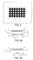
- Fig. 2 is a schematic view showing a granular structure of M-X-Y magnetic composition;
- Fig. 3A is a schematic sectional view showing a structure of a sputtering apparatus which was used in examples;
- Fig. 3B is a schematic sectional view showing a structure of a vapor deposition apparatus which was used in examples;
- Fig. 4 is a graphical view showing a permeability frequency response of
film sample 1 in Example 1; - Fig. 5 is a graphical view showing a permeability frequency response of
film sample 2 in Example 2; - Fig. 6 is a graphical view showing a permeability frequency response of
comparable sample 1 in Comparable Example 1; - Fig. 7 is a schematic and perspective view of a test apparatus for testing an noise suppressing effect of magnetic samples;
- Fig. 8A is a graphic view showing a transmission characteristic of
film sample 1; - Fig. 8B is a graphic view showing a transmission characteristic of comparable sample of composite magnetic material sheet;
- Fig. 9A is a distribution constant circuit with a length ℓ showing a magnetic material as a noise suppressor;
- Fig. 9B is an equivalent circuit with a unit length Δℓ of the distribution constant circuit of Fig. 9A;
- Fig. 9C is an equivalent circuit with a length ℓ of the distribution constant circuit of Fig. 9A;
- Fig. 10A is a graphic view showing a frequency response of an
equivalent resistance R of
film sample 1 in Example 1; and - Fig. 10B is a graphic view showing a frequency response of an equivalent resistance R of comparative sample of a composite magnetic material sheet.
-
- Referring to Fig. 1, description will be made of a resin-molded unit according to one embodiment of this invention.
- The resin-molded unit is depicted by a
reference numeral 1 and contains asemiconductor bear chip 2 arranged inside and sealed in anepoxy resin mold 3. From thesemiconductor bear chip 2, a plurality oflead frames 4 are extracted through theepoxy resin mold 3 to the outside. - Furthermore, the
epoxy resin mold 3 is entirely covered with a high-frequencycurrent suppressor 5. The high-frequency current suppressor 5 is a thin film magnetic substance formed in the form of a film by sputtering or vapor deposition known in the art, having a thickness between 0.3 µm and 20 µm, and exhibiting the conductivity in a frequency band lower than several tens MHz. The high-frequency current suppressor 5 serves to attenuate a high-frequency current flowing through a circuit portion inside theepoxy resin mold 3 and having a frequency within a frequency band between several tens MHz and several GHz. - Upon forming the high-frequency
current suppressor 5, use may be made of chemical vapor deposition (CVD), ion beam deposition, gas deposition, and pattern transfer in addition to the sputtering or the vapor deposition mentioned above. - As a material for each of the high-frequency
current suppressors 4a, 4b, and 5, use may be made of a narrow-band magnetic loss material which has an M-X-Y composition as a mixture of components or elements M (M being at least one of Fe, Co, and Ni), Y (Y being at least one of F, N, and O), and X (X being at least one element other than those contained in M and Y) and which has a permeability characteristic, given as a relationship between a frequency and an imaginary part µ" with respect to a real part µ' of relative permeability, such that the maximum value µ"max of the imaginary part µ" (which may be called a magnetic loss term) is present within a frequency range between 100MHz and 10GHz and that a relative bandwidth bwr is not greater than 200% where the relative bandwidth bwr is obtained by extracting a frequency bandwidth between two frequencies at which the value of µ" is 50% of the maximum µ"max and normalizing the frequency bandwidth at the center frequency thereof. It is assumed here that the narrow-band magnetic loss material has saturation magnetization between 80% and 60% of that of a metal magnetic material comprising the component M alone and a d.c. electric resistance between 100 µ Ω · cm and 700 µ Ω · cm. - As the material for each of the high-frequency
current suppressors 4a, 4b, and 5, use may also be made of a wide-band magnetic loss material which has an M-X-Y composition as a mixture of components M (M being at least one of Fe, Co, and Ni), Y (Y being at least one of F, N, and O), and X (X being at least one element other than those contained in M and Y) and which has a permeability characteristic, given as a relationship between a frequency and an imaginary part µ" with respect to a real part µ' of relative permeability, such that the maximum value µ"max of the imaginary part µ" is present within a frequency range between 100MHz and 10GHz and that a relative bandwidth bwr is not smaller than 150% where the relative bandwidth bwr is obtained by extracting a frequency bandwidth between two frequencies at which the value of µ" is 50% of the maximum µ "max and normalizing the frequency bandwidth at the center frequency thereof. It is assumed here that the wide-band magnetic loss material has saturation magnetization between 60% and 35% of that of a metal magnetic material comprising the component M alone and a d.c. electric resistance greater than 500 µ Ω · cm. - In each of the narrow-band magnetic loss material and the wide-band magnetic loss material used as the high-frequency
current suppressors 4a, 4b, and 5, the component X is at least one of C, B, Si, Al, Mg, Ti, Zn, Hf, Sr, Nb, Ta, and rare earth elements. The component M is present in a granular structure where particles or grains of the component M are dispersed in a matrix of a compound of the components X and Y. The particles have an average particle size between 1 nm and 40nm. The narrow-band or the wide-band magnetic loss material has an anisotropic magnetic field of 47400 A/m or less. Preferably, the M-X-Y composition of the wide-band or the narrow-band magnetic loss material is an Fe-Al-O composition or an Fe-Si-O composition. - The resin-molded
unit 1 is similar in appearance to that of the conventional product but is superior in effect. Specifically, even in occurrence of a harmonic current as an undesired harmonic having a frequency ranging from several tens MHz to several GHz, such high-frequency can be sufficiently attenuated by the high-frequencycurrent suppressor 5. As a result, production of a high-frequency noise can be prevented so as to remove an adverse affect by the high-frequency noise. - As the high-frequency
current suppressor 5, use is made of a thin-film magnetic substance which is small in volume and therefore requires less space and which is a magnetic loss material having a large imaginary part (i.e., a "magnetic loss term") µ" of relative permeability so as to provide effective protection against undesired radiation. As a magnetic substance which shows large magnetic loss, a granular magnetic material is known. Specifically, in case where the concentration of magnetic metal particles in the granular magnetic material falls within a particular range, excellent magnetic loss characteristic can be obtained in a high-frequency region. - Next, description will be made as to granular structure and production methods of M-X-Y magnetic composition.
- Referring to Fig. 2 in which schematically shows the granular structure of M-X-Y magnetic composition,
particles 11 of metallic magnetic material M are uniformly or evenly distributed in amatrix 12 consisting of X and Y. - Referring to Fig. 3A, a sputtering apparatus shown therein was used for producing samples in the following examples and comparative examples. The sputtering apparatus has a conventional structure and comprises a
vacuum container 20, ashutter 21, anatmospheric gas source 22, a substrate or aglass plate 23, chips 24 (X or X-Y), a target 25 (M), an RF power source, and avacuum pump 27. Theatmospheric gas source 22 and thevacuum pump 27 are connected to thevacuum container 20. Thesubstrate 23 confronts to thetarget 25 on which chips 24 are disposed. Theshutter 21 is disposed in front of thesubstrate 21. TheRF power source 26 is connected to thetarget 25. - Referring to Fig. 3B, a vapor deposition apparatus shown therein was also used another apparatus for producing samples in the following examples and comparative examples. The vapor deposition apparatus has a conventional structure and has
vacuum container 20,atmospheric gas source 22, andvacuum pump 27 similar to the sputtering apparatus but has acrucible 28 including materials (X-Y) in place ofchips 24,target 25 andRF power source 26. - A thin film of M-X-Y magnetic composition was made on a glass plate by use of the sputtering apparatus shown in Fig. 3A at a sputtering condition shown in Table 1.
Vacuum degree before sputtering <1 × 10⁻⁶ Torr Atmosphere Ar gas Electric Power RF Targets Fe (diameter of 100mm) and Al2O3 chip (120 pieces) (chip size: 5mm × 5mm × 2mm) - The
film sample 1 produced was analyzed by a fluorescent X-ray spectroscopy and confirmed as a film of a composition Fe72Al11O17. Thefilm sample 1 had 2.0 micrometer (µm) in thickness, 530 micro ohm centimeters (µ Ω • cm) in DC specific resistance, 18 Oe in anisotropy field (Hk), and 16,800 Gauss in saturation magnetization (Ms). - A percent ratio of the saturation magnetization of the
film sample 1 and that of the metallic material M itself {Ms(M-X-Y)/Ms(M)}× 100 was 72.2%. - In order to measure a permeability frequency response, the
film sample 1 was formed in a ribbon like form and inserted in a coil. Under application of a bias magnetic field, an impedance variation of the coil was measured in response to frequency change of AC current applied to the coil. The measurement was several times for different values of the bias magnetic field. From the measured impedance variation in response to frequency variation, the permeability frequency response (µ"-f response) was calculated and is shown in Fig. 4. It will be noted from Fig. 4 that the imaginary part of relative permeability has a high peak or the maximum value (µ"max) and rapidly falls either side of the peak. The natural resonance frequency (f(µ"max)) showing the maximum value (µ"max) is about 700 MHz. From the µ"-f response, a relative bandwidth bwr was determined as a percentage ratio of bandwidth between two frequency points which shows the imaginary part of relative permeability as a half value µ"50 of the maximum value µ"max, to center frequency of said bandwidth. The relative bandwidth bwr was 148%. - In a condition similar to that in Example 1 but using of 150 Al2O3 chips, a
film sample 2 was formed on a glass plate. - The
film sample 2 produced was analyzed by a fluorescent X-ray spectroscopy and confirmed as a film of a composition Fe44Al22O34. Thefilm sample 2 had 1.2 micrometer (µm) in thickness, 2400 micro ohm centimeters (µ Ω · cm) in DC specific resistance, 120 Oe in anisotropy field (Hk), and 9600 Gauss in saturation magnetization (Ms). It will be noted thatfilm sample 2 is higher thanfilm sample 1 in the specific resistance. - A percent ratio of the saturation magnetization of the
film sample 2 and that of the metallic material M itself {Ms(M-X-Y)/Ms(M)}× 100 was 44.5%. - The µ"-f response of
film sample 2 was also obtained in the similar manner as in Example 1 and shows in Fig. 5. It is noted that the peak has also a high value similar to that infilm sample 1. However, the frequency point at the peak, or the natural resonance frequency is about 1 GHz and the imaginary part of relative permeability gradually falls either side of the peak so that the µ"-f response has a broadband characteristic. - A relative bandwidth bwr of
film sample 2 was also confirmed as 181% by the similar way as in Example 1. - In a condition similar to that in Example 1 but using of 90 Al2O3 chips, a
comparative sample 1 was formed on a glass plate. - The
comparative sample 1 produced was analyzed by a fluorescent X-ray spectroscopy and confirmed as a film of a composition Fe86Al6O8. Thecomparative sample 1 had 1.2 micrometer (µm) in thickness, 74 micro ohm centimeters (µ Ω • cm) in DC specific resistance, 22 Oe in anisotropy field (Hk), 18,800 Gauss in saturation magnetization (Ms), and 85.7% in a percent ratio of the saturation magnetization of thecomparative sample 1 and that of the metallic material M itself {Ms(M-X-Y)/Ms(M)}× 100, and. was 44.5%. - The µ"-f response of
comparative sample 1 was also obtained in the similar manner as in Example 1, and is shown in Fig. 6. It will be noted from Fig. 6 that the imaginary part µ" of relative permeability of thecomparative sample 1 has a high peak at a frequency about 10 MHz but rapidly reduces at the higher frequency range than 10 MHz. It can be supposed that this reduction is caused by generation of eddy current due to the lower specific resistance. - In a condition similar to that in Example 1 but using of 200 Al2O3 chips, a
comparative sample 2 was formed on a glass plate. - The
comparative sample 2 produced was analyzed by a fluorescent X-ray spectroscopy and confirmed as a film of a composition Fe19Al34O47. Thecomparative sample 2 had 1.3 micrometer (µm) in thickness, 10,500 micro ohm centimeters (µ Ω • cm) in DC specific resistance. - The magnetic characteristic of
comparative sample 1 exhibited superparamagnetism. - A thin film of M-X-Y magnetic composition was made on a glass plate by the reactive sputtering method using the sputtering apparatus shown in Fig. 3A at a sputtering condition shown in Table 2. The partial pressure ratio of N2 was 20%. The thin film was heat-treated at a temperature of 300°C for two hours in vacuum under magnetic field and obtained a
film sample 4.Vacuum degree before sputtering <1 × 10⁻⁶ Torr Atmosphere Ar+N2 gas Electric Power RF Targets Fe (diameter of 100mm) and Al chip (150 pieces) (chip size: 5mm × 5mm × 2mm) - The properties of
film sample 4 are show in Table 3.Film thickness 1.5 µm {Ms(M-X-Y)/Ms(M)}× 100 51.9% µ"max 520 f(µ"max) 830MHz bwr 175% - A thin film of M-X-Y magnetic composition was made on a glass plate by using the sputtering apparatus shown in Fig. 3A at a sputtering condition shown in Table 4. The thin film was heat-treated at a temperature of 300°C for two hours in vacuum under magnetic field and obtained a
film sample 5.Vacuum degree before sputtering <1 × 10⁻⁶ Torr Atmosphere Ar gas Electric Power RF Targets Co (diameter of 100mm) and Al2O3 chip (130 pieces) (chip size: 5mm × 5mm × 2mm) - The properties of
film sample 5 are show in Table 5.Film thickness 1.1 µm {Ms(M-X-Y)/Ms(M)}× 100 64.7% µ"max 850 f(µ"max) 800MHz bwr 157% - A thin film of M-X-Y magnetic composition was made on a glass plate by the reactive sputtering method using the sputtering apparatus shown in Fig. 3A at a sputtering condition shown in Table 6. The partial pressure ratio of N2 was 10%. The thin film was heat-treated at a temperature of 300°C for two hours in vacuum under magnetic field and obtained a film sample 6.
Vacuum degree before sputtering <1 × 10⁻⁶ Torr Atmosphere Ar+N2 gas Electric Power RF Targets Co (diameter of 100mm) and Al chip (170 pieces) (chip size: 5mm × 5mm × 2mm) - The properties of film sample 6 are show in Table 7.
Film thickness 1.2 µm {Ms(M-X-Y)/Ms(M)}× 100 32.7% µ"max 350 f(µ"max) 1GHz bwr 191% - A thin film of M-X-Y magnetic composition was made on a glass plate by using the sputtering apparatus shown in Fig. 3A at a sputtering condition shown in Table 8. The thin film was heat-treated at a temperature of 300°C for two hours in vacuum under magnetic field and obtained a film sample 7.
Vacuum degree before sputtering <1 × 10⁻⁶ Torr Atmosphere Ar gas Electric Power RF Targets Ni (diameter of 100mm) and Al2O3 chip (140 pieces) (chip size: 5mm × 5mm × 2mm) - The properties of
film sample 4 are show in Table 9.Film thickness 1.7 µm {Ms(M-X-Y)/Ms(M)}× 100 58.2% µ"max 280 f(µ"max) 240MHz bwr 169% - A thin film of M-X-Y magnetic composition was made on a glass plate by the reactive sputtering method using the sputtering apparatus shown in Fig. 3A at a sputtering condition shown in Table 10. The partial pressure ratio of N2 was 10%. The thin film was heat-treated at a temperature of 300°C for two hours in vacuum under magnetic field and obtained a film sample 8.
Vacuum degree before sputtering <1 × 10⁻⁶ Torr Atmosphere Ar+N2 gas Electric Power RF Targets Ni (diameter of 100mm) and Al chip (100 pieces) (chip size: 5mm × 5mm × 2mm) - The properties of
film sample 10 are show in Table 11.Film thickness 1.3 µm {Ms(M-X-Y)/Ms(M)}× 100 76.2% µ"max 410 f(µ"max) 170MHz bwr 158% - A thin film of M-X-Y magnetic composition was made on a glass plate by using the sputtering apparatus shown in Fig. 3A at a sputtering condition shown in Table 12. The thin film was heat-treated at a temperature of 300°C for two hours in vacuum under magnetic field and obtained a film sample 9.
Vacuum degree before sputtering <1 × 10⁻⁶ Torr Atmosphere Ar gas Electric Power RF Targets Fe (diameter of 100mm) and TiO2 chip (150 pieces) (chip size: 5mm × 5mm × 2mm) - The properties of film sample 9 are show in Table 13.
Film thickness 1.4 µm {Ms(M-X-Y)/Ms(M)}× 100 43.6% µ"max 920 f(µ"max) 1.5GHz bwr 188% - A thin film of M-X-Y magnetic composition was made on a glass plate by the reactive sputtering method using the sputtering apparatus shown in Fig. 3A at a sputtering condition shown in Table 14. The partial pressure ratio of O2 was 15%. The thin film was heat-treated at a temperature of 300°C for two hours in vacuum under magnetic field and obtained a
film sample 10.Vacuum degree before sputtering <1 × 10⁻⁶ Torr Atmosphere Ar+O2 gas Electric Power RF Targets Fe (diameter of 100mm) and Si chip (130 pieces) (chip size: 5mm × 5mm × 2mm) - The properties of
film sample 10 are show in Table 15.Film thickness 1.5 µm {Ms(M-X-Y)/Ms(M)}×100 55.2% µ"max 920 f(µ"max) 1.2GHz bwr 182% - A thin film of M-X-Y magnetic composition was made on a glass plate by using the sputtering apparatus shown in Fig. 3A at a sputtering condition shown in Table 16. The thin film was heat-treated at a temperature of 300°C for two hours in vacuum under magnetic field and obtained a
film sample 11.Vacuum degree before sputtering <1 × 10⁻⁶ Torr Atmosphere Ar gas Electric Power RF Targets Fe (diameter of 100mm) and HfO3 chip (100 pieces) (chip size: 5mm × 5mm × 2mm) - The properties of
film sample 11 are show in Table 17.Film thickness 1.8 µm {Ms(M-X-Y)/Ms(M)}× 100 77.4% µ"max 1800 f(µ"max) 450MHz bwr 171% - A thin film of M-X-Y magnetic composition was made on a glass plate by using the sputtering apparatus shown in Fig. 3A at a sputtering condition shown in Table 18. The thin film was heat-treated at a temperature of 300°C for two hours in vacuum under magnetic field and obtained a
film sample 12.Vacuum degree before sputtering <1 × 10⁻⁶ Torr Atmosphere Ar gas Electric Power RF Targets Fe (diameter of 100mm) and BN chip (130 pieces) (chip size: 5mm×5mm×2mm) - The properties of
film sample 12 are show in Table 19.Film thickness 1.9 µm {Ms(M-X-Y)/Ms(M)} × 100 59.3% µ"max 950 f(µ"max) 680MHz bwr 185% - A thin film of M-X-Y magnetic composition was made on a glass plate by using the sputtering apparatus shown in Fig. 3A at a sputtering condition shown in Table 20. The thin film was heat-treated at a temperature of 300°C for two hours in vacuum under magnetic field and obtained a film sample 13.
Vacuum degree before sputtering <1 × 10⁻⁶ Torr Atmosphere Ar gas Electric Power RF Targets Fe50Co50 (diameter of 100mm) and Al2O3 chip (130 pieces) (chip size: 5mm × 5mm × 2mm) - The properties of film sample 13 are show in Table 21.
Film thickness 1.6 µm {Ms(M-X-Y)/Ms(M)}×100 59.3% µ"max 720 f(µ"max) 1.1GHz bwr 180% - A thin film of M-X-Y magnetic composition was made on a glass plate by using the vapor deposition apparatus shown in Fig. 3B at a condition shown in Table 22. The thin film was heat-treated at a temperature of 300°C for two hours in vacuum under magnetic field and obtained a film sample 14.
Vacuum degree before sputtering <1 × 10⁻⁶ Torr Atmosphere flowing rate O2 at 3.0 sccm Elements in crucible Fe and Al - The properties of film sample 14 are show in Table 23.
Film thickness 1.1 µm {Ms(M-X-Y)/Ms(M)}× 100 41.8% µ"max 590 f(µ"max) 520MHz bwr 190% - Now, description will be made as to tests relating to noise suppressing effect of sample films and comparative samples, using a test apparatus shown in Fig. 7.
- A test piece was
film sample 1 with dimensions of 20mm × 20mm × 2.0 µm. For a comparison, a sheet of known composite magnetic material having dimensions of 20mm × 20mm × 1.0mm. The composite magnetic material comprising polymer and flat magnetic metal powder dispersed in the polymer. The magnetic metal powder comprises Fe, Al and Si. The composite magnetic material has a permeability distribution in quasi-microwave range and has the maximum value of the imaginary part of relative permeability at a frequency about 700 MHz. Table 24 shows magnetic properties of both of the test piece and comparative test piece.Film sample 1Comparative test piece µ"/700MHz about 1800 about 3.0 bwr 148 196 - As seen from Table 24, the
film sample 1 is about 600 times more than comparative test piece in the maximum value of imaginary part of relative permeability. Since the noise suppressing effect is generally evaluated from a value of a product (µ"max × δ) of the maximum value µ"max of the imaginary part of relative permeability and thickness of the piece δ, the thickness of the comparative test piece of the composite magnetic material sheet was selected 1 mm so that the both of test pieces have the similar values of (µ"max× δ). - Referring to Fig. 7, the test apparatus comprises a
micro-strip line 61 having two ports,coaxial cables 62 connected to the two ports, and a network analyzer (not shown) connected across the two ports. Themicro-strip line 61 has a line length of 75mm and a characteristic impedance of 50 ohms. Thetest piece 63 was disposed at aregion 64 on themicro-strip line 61 and the transmission characteristic S21 was measured. The frequency response of S21 are shown in Figs. 8A and 8B forfilm sample 1 and the comparative sample, respectively. - With respect to use of
film sample 1, it will be noted from Fig. 8A that S21 reduces above 100 MHz, becomes to the minimum of -10dB at a frequency of 2 GHz and then increases above 2 GHz. On the other hand, with respect to use of comparative sample, it will be noted from Fig. 8B that S21 gradually reduces and becomes to the minimum of -10dB at a frequency of 3GHz. - The results demonstrate that S21 is dependent on the frequency distribution of the permeability and that the noise suppressing effect is dependent on the product of (µ"max × δ).
- Now, providing that the magnetic sample forms a distribution constant circuit having a length of ℓ as shown in Fig. 9A, an equivalent circuit was calculated for a unit length of Δℓ from transmission characteristics S11 and S21, as shown in Fig. 9B. Then, the equivalent circuit for the length ℓ was obtained from the equivalent circuit for the unit length Δℓ, as shown in Fig. 9C. The equivalent circuit of the magnetic sample comprises series inductance L and resistance R and parallel capacitance C and conductance G, as shown in Fig. 9C. From this, it will be understood that the change of transmission characteristic of the micro-strip line caused due to disposition of the magnetic substance on the micro-strip line is mainly determined by the equivalent resistance R added in series.
- In view of the above, a frequency response of the equivalent resistance R was measured. The measured data were shown in Figs. 10A and 10B for the
film sample 1 and the comparative sample, respectively. It will be noted from these figures that the equivalent resistance R gradually reduces in the quasi-microwave range and is about 60 ohms at about 3 GHz. It is seen that the frequency dependency of the equivalent resistance R is different from that of the imaginary part of relative permeability which has the maximum value at about 1 GHz. It will be supposed that this difference will be based on the gradual increase of a ratio of the product and the sample length to the wavelength.
Claims (9)
- A resin-molded unit comprising:an electronic circuit component;a resin molding said electronic circuit component therein; anda high-frequency current suppressor covering at least one part of said resin, said high-frequency current suppressor being made of a magnetic loss film.
- A resin-molded unit as claimed in claim 1, wherein said electronic circuit component is a semiconductor chip.
- A resin-molded unit as claimed in claim 1 or 2, wherein said high-frequency current suppressor is a magnetic substance which shows large magnetic loss.
- A resin-molded unit as claimed in any one of claims 1 to 3, wherein said magnetic loss film is made of a granular magnetic material.
- A resin-molded unit as claimed in claim 4, wherein said granular magnetic material is deposited on said at least one of said resin by sputtering.
- A resin-molded unit as claimed in claim 4, wherein said granular magnetic material is a deposited on said at least one of said resin by vapor deposition.
- A resin-molded unit as claimed in any one of claims 1-6, wherein said magnetic loss film serves to attenuate a high-frequency current flowing through said electronic circuit component and having a frequency within a frequency band between several tens MHz and several GHz.
- A resin-molded unit as claimed in any one of claims 1-7, wherein said magnetic loss film is made of a magnetic substance of a magnetic composition comprising M, X and Y, where M is a metallic magnetic material consisting of Fe, Co, and/or Ni, X being element or elements other than M and Y, and Y being F, N, and/or O, said M-X-Y magnetic composition having a concentration of M in the composition so that said M-X-Y magnetic composition has a saturation magnetization of 35-80% of that of the metallic bulk of magnetic material comprising M alone, said magnetic composition having the maximum value µ"max of an imaginary part of relative permeability µ" in a frequency range of 0.1-10 gigahertz (GHz).
- A resin-molded unit as claimed in claim 8, which has a permeability frequency response of a relatively broad band where a relative bandwidth bwr is 150% or more, said relative bandwidth bwr is determined as a percentage ratio of bandwidth between two frequency points which shows the imaginary part of relative permeability as a half value µ"50 of the maximum µ"max, to center frequency of said bandwidth.
Applications Claiming Priority (2)
| Application Number | Priority Date | Filing Date | Title |
|---|---|---|---|
| JP2000102378 | 2000-04-04 | ||
| JP2000102378A JP4398056B2 (en) | 2000-04-04 | 2000-04-04 | Resin mold body |
Publications (1)
| Publication Number | Publication Date |
|---|---|
| EP1143518A1 true EP1143518A1 (en) | 2001-10-10 |
Family
ID=18616274
Family Applications (1)
| Application Number | Title | Priority Date | Filing Date |
|---|---|---|---|
| EP01108513A Withdrawn EP1143518A1 (en) | 2000-04-04 | 2001-04-04 | Resin-molded unit including an electronic circuit component covered by a protective magnetic film |
Country Status (7)
| Country | Link |
|---|---|
| US (1) | US6495927B2 (en) |
| EP (1) | EP1143518A1 (en) |
| JP (1) | JP4398056B2 (en) |
| KR (1) | KR20010095273A (en) |
| CN (1) | CN1316778A (en) |
| NO (1) | NO20011708L (en) |
| TW (1) | TW504829B (en) |
Cited By (1)
| Publication number | Priority date | Publication date | Assignee | Title |
|---|---|---|---|---|
| FR2852190A1 (en) * | 2003-03-03 | 2004-09-10 | Wavecom | METHOD FOR MANUFACTURING AN ELECTRONIC COMPONENT OR MODULE AND CORRESPONDING COMPONENT OR MODULE |
Families Citing this family (13)
| Publication number | Priority date | Publication date | Assignee | Title |
|---|---|---|---|---|
| KR20010095252A (en) * | 2000-04-04 | 2001-11-03 | 도낀 가부시끼가이샤 | Electronic component of a high frequency current suppression type and bonding wire for the same |
| US6967390B2 (en) * | 2003-02-13 | 2005-11-22 | Freescale Semiconductor, Inc. | Electronic component and method of manufacturing same |
| US7968978B2 (en) * | 2007-06-14 | 2011-06-28 | Raytheon Company | Microwave integrated circuit package and method for forming such package |
| KR100877551B1 (en) * | 2008-05-30 | 2009-01-07 | 윤점채 | Semiconductor package having electromagnetic shielding function, manufacturing method and jig |
| US8592967B2 (en) * | 2009-01-28 | 2013-11-26 | Hitachi Metals, Ltd. | Semiconductor apparatus and power supply circuit |
| CN104220954B (en) * | 2012-05-17 | 2018-07-17 | 英特尔公司 | Thin Film Insert Molding for Device Manufacturing |
| WO2015057209A1 (en) * | 2013-10-15 | 2015-04-23 | Intel Corporation | Magnetic shielded integrated circuit package |
| US10242954B2 (en) * | 2016-12-01 | 2019-03-26 | Tdk Corporation | Electronic circuit package having high composite shielding effect |
| US9881877B2 (en) | 2016-03-31 | 2018-01-30 | Tdk Corporation | Electronic circuit package using composite magnetic sealing material |
| US9818518B2 (en) | 2016-03-31 | 2017-11-14 | Tdk Corporation | Composite magnetic sealing material |
| US9972579B1 (en) | 2016-11-16 | 2018-05-15 | Tdk Corporation | Composite magnetic sealing material and electronic circuit package using the same |
| US10403582B2 (en) | 2017-06-23 | 2019-09-03 | Tdk Corporation | Electronic circuit package using composite magnetic sealing material |
| JP7788972B2 (en) * | 2022-09-13 | 2025-12-19 | 株式会社東芝 | Isolator |
Citations (5)
| Publication number | Priority date | Publication date | Assignee | Title |
|---|---|---|---|---|
| US5220298A (en) * | 1990-07-24 | 1993-06-15 | Kabushiki Kaisha Toshiba | Integrated circuit having a built-in noise filter |
| US5639989A (en) * | 1994-04-19 | 1997-06-17 | Motorola Inc. | Shielded electronic component assembly and method for making the same |
| EP0859378A1 (en) * | 1996-08-23 | 1998-08-19 | Tokin Corporation | Emi preventive part and active device with the same |
| US5864088A (en) * | 1994-01-20 | 1999-01-26 | Tokin Corporation | Electronic device having the electromagnetic interference suppressing body |
| EP0897256A1 (en) * | 1996-04-24 | 1999-02-17 | Okamura, Susumu | Semiconductor device |
Family Cites Families (2)
| Publication number | Priority date | Publication date | Assignee | Title |
|---|---|---|---|---|
| JPH0323654A (en) * | 1989-06-21 | 1991-01-31 | Mitsubishi Electric Corp | Resin-sealed semiconductor device |
| US5370766A (en) * | 1993-08-16 | 1994-12-06 | California Micro Devices | Methods for fabrication of thin film inductors, inductor networks and integration with other passive and active devices |
-
2000
- 2000-04-04 JP JP2000102378A patent/JP4398056B2/en not_active Expired - Fee Related
-
2001
- 2001-04-03 KR KR1020010017663A patent/KR20010095273A/en not_active Withdrawn
- 2001-04-03 US US09/825,420 patent/US6495927B2/en not_active Expired - Fee Related
- 2001-04-04 TW TW090108094A patent/TW504829B/en not_active IP Right Cessation
- 2001-04-04 CN CN01116567A patent/CN1316778A/en active Pending
- 2001-04-04 NO NO20011708A patent/NO20011708L/en not_active Application Discontinuation
- 2001-04-04 EP EP01108513A patent/EP1143518A1/en not_active Withdrawn
Patent Citations (5)
| Publication number | Priority date | Publication date | Assignee | Title |
|---|---|---|---|---|
| US5220298A (en) * | 1990-07-24 | 1993-06-15 | Kabushiki Kaisha Toshiba | Integrated circuit having a built-in noise filter |
| US5864088A (en) * | 1994-01-20 | 1999-01-26 | Tokin Corporation | Electronic device having the electromagnetic interference suppressing body |
| US5639989A (en) * | 1994-04-19 | 1997-06-17 | Motorola Inc. | Shielded electronic component assembly and method for making the same |
| EP0897256A1 (en) * | 1996-04-24 | 1999-02-17 | Okamura, Susumu | Semiconductor device |
| EP0859378A1 (en) * | 1996-08-23 | 1998-08-19 | Tokin Corporation | Emi preventive part and active device with the same |
Cited By (2)
| Publication number | Priority date | Publication date | Assignee | Title |
|---|---|---|---|---|
| FR2852190A1 (en) * | 2003-03-03 | 2004-09-10 | Wavecom | METHOD FOR MANUFACTURING AN ELECTRONIC COMPONENT OR MODULE AND CORRESPONDING COMPONENT OR MODULE |
| WO2004082022A3 (en) * | 2003-03-03 | 2005-09-15 | Wavecom | Method for producing an electronic component or module and a corresponding component or module |
Also Published As
| Publication number | Publication date |
|---|---|
| JP4398056B2 (en) | 2010-01-13 |
| NO20011708L (en) | 2001-10-05 |
| KR20010095273A (en) | 2001-11-03 |
| CN1316778A (en) | 2001-10-10 |
| JP2001284498A (en) | 2001-10-12 |
| US20010035579A1 (en) | 2001-11-01 |
| TW504829B (en) | 2002-10-01 |
| US6495927B2 (en) | 2002-12-17 |
| NO20011708D0 (en) | 2001-04-04 |
Similar Documents
| Publication | Publication Date | Title |
|---|---|---|
| US6595802B1 (en) | Connector capable of considerably suppressing a high-frequency current | |
| EP1143458B1 (en) | Signal transmission cable with a noise absorbing high loss magnetic film formed on a sheath of the cable | |
| US6495927B2 (en) | Resin-molded unit including an electronic circuit component | |
| KR20010098654A (en) | High-frequency current suppression body using magnetic loss material exhibiting outstanding complex permeability characteristics | |
| EP1166997A1 (en) | Heat-shrinkable tube, heat-shrinkable sheet, and method of shrinking the same | |
| KR20010095320A (en) | Wiring board comprising granular magnetic film | |
| US6635819B2 (en) | Electronic component comprising a metallic case provided with a magnetic loss material | |
| EP1146637B1 (en) | Electronic component of a high frequency current suppression type and bonding wire for the same | |
| JP2001284878A (en) | Wiring board | |
| EP1143777B1 (en) | Cooling device capable of considerably suppressing a high-frequency current flowing in an electric component | |
| EP1166288B1 (en) | Magnetic substance with maximum complex permeability in quasi-microwave band and method for production of the same | |
| JP4398057B2 (en) | High frequency current suppression type electronic components | |
| JP4243000B2 (en) | High frequency current suppressing bonding wire for electronic components and electronic component including the same | |
| JP2001284947A (en) | Antenna using high frequency current suppressor |
Legal Events
| Date | Code | Title | Description |
|---|---|---|---|
| PUAI | Public reference made under article 153(3) epc to a published international application that has entered the european phase |
Free format text: ORIGINAL CODE: 0009012 |
|
| AK | Designated contracting states |
Kind code of ref document: A1 Designated state(s): DE FI FR GB SE Kind code of ref document: A1 Designated state(s): AT BE CH CY DE DK ES FI FR GB GR IE IT LI LU MC NL PT SE TR |
|
| AX | Request for extension of the european patent |
Free format text: AL;LT;LV;MK;RO;SI |
|
| 17P | Request for examination filed |
Effective date: 20020322 |
|
| AKX | Designation fees paid |
Free format text: DE FI FR GB SE |
|
| 17Q | First examination report despatched |
Effective date: 20020621 |
|
| RAP1 | Party data changed (applicant data changed or rights of an application transferred) |
Owner name: NEC TOKIN CORPORATION |
|
| GRAP | Despatch of communication of intention to grant a patent |
Free format text: ORIGINAL CODE: EPIDOSNIGR1 |
|
| STAA | Information on the status of an ep patent application or granted ep patent |
Free format text: STATUS: THE APPLICATION IS DEEMED TO BE WITHDRAWN |
|
| 18D | Application deemed to be withdrawn |
Effective date: 20051129 |