EP1139498A2 - Electrical connector with grounding system - Google Patents
Electrical connector with grounding system Download PDFInfo
- Publication number
- EP1139498A2 EP1139498A2 EP01107457A EP01107457A EP1139498A2 EP 1139498 A2 EP1139498 A2 EP 1139498A2 EP 01107457 A EP01107457 A EP 01107457A EP 01107457 A EP01107457 A EP 01107457A EP 1139498 A2 EP1139498 A2 EP 1139498A2
- Authority
- EP
- European Patent Office
- Prior art keywords
- contacts
- paired
- electrical connector
- signal
- ground
- Prior art date
- Legal status (The legal status is an assumption and is not a legal conclusion. Google has not performed a legal analysis and makes no representation as to the accuracy of the status listed.)
- Granted
Links
Images







Classifications
-
- H—ELECTRICITY
- H01—ELECTRIC ELEMENTS
- H01R—ELECTRICALLY-CONDUCTIVE CONNECTIONS; STRUCTURAL ASSOCIATIONS OF A PLURALITY OF MUTUALLY-INSULATED ELECTRICAL CONNECTING ELEMENTS; COUPLING DEVICES; CURRENT COLLECTORS
- H01R13/00—Details of coupling devices of the kinds covered by groups H01R12/70 or H01R24/00 - H01R33/00
- H01R13/648—Protective earth or shield arrangements on coupling devices, e.g. anti-static shielding
-
- H—ELECTRICITY
- H01—ELECTRIC ELEMENTS
- H01R—ELECTRICALLY-CONDUCTIVE CONNECTIONS; STRUCTURAL ASSOCIATIONS OF A PLURALITY OF MUTUALLY-INSULATED ELECTRICAL CONNECTING ELEMENTS; COUPLING DEVICES; CURRENT COLLECTORS
- H01R13/00—Details of coupling devices of the kinds covered by groups H01R12/70 or H01R24/00 - H01R33/00
- H01R13/02—Contact members
- H01R13/22—Contacts for co-operating by abutting
- H01R13/24—Contacts for co-operating by abutting resilient; resiliently-mounted
- H01R13/2407—Contacts for co-operating by abutting resilient; resiliently-mounted characterized by the resilient means
- H01R13/2414—Contacts for co-operating by abutting resilient; resiliently-mounted characterized by the resilient means conductive elastomers
-
- H—ELECTRICITY
- H01—ELECTRIC ELEMENTS
- H01R—ELECTRICALLY-CONDUCTIVE CONNECTIONS; STRUCTURAL ASSOCIATIONS OF A PLURALITY OF MUTUALLY-INSULATED ELECTRICAL CONNECTING ELEMENTS; COUPLING DEVICES; CURRENT COLLECTORS
- H01R12/00—Structural associations of a plurality of mutually-insulated electrical connecting elements, specially adapted for printed circuits, e.g. printed circuit boards [PCB], flat or ribbon cables, or like generally planar structures, e.g. terminal strips, terminal blocks; Coupling devices specially adapted for printed circuits, flat or ribbon cables, or like generally planar structures; Terminals specially adapted for contact with, or insertion into, printed circuits, flat or ribbon cables, or like generally planar structures
- H01R12/70—Coupling devices
- H01R12/71—Coupling devices for rigid printing circuits or like structures
- H01R12/72—Coupling devices for rigid printing circuits or like structures coupling with the edge of the rigid printed circuits or like structures
- H01R12/722—Coupling devices for rigid printing circuits or like structures coupling with the edge of the rigid printed circuits or like structures coupling devices mounted on the edge of the printed circuits
- H01R12/727—Coupling devices presenting arrays of contacts
-
- H—ELECTRICITY
- H01—ELECTRIC ELEMENTS
- H01R—ELECTRICALLY-CONDUCTIVE CONNECTIONS; STRUCTURAL ASSOCIATIONS OF A PLURALITY OF MUTUALLY-INSULATED ELECTRICAL CONNECTING ELEMENTS; COUPLING DEVICES; CURRENT COLLECTORS
- H01R13/00—Details of coupling devices of the kinds covered by groups H01R12/70 or H01R24/00 - H01R33/00
- H01R13/648—Protective earth or shield arrangements on coupling devices, e.g. anti-static shielding
- H01R13/658—High frequency shielding arrangements, e.g. against EMI [Electro-Magnetic Interference] or EMP [Electro-Magnetic Pulse]
- H01R13/6581—Shield structure
- H01R13/6585—Shielding material individually surrounding or interposed between mutually spaced contacts
Definitions
- the present invention relates to electrical connectors and, more particularly, to an electrical connector having center ground contacts.
- U.S. Patents 5,429,520 and 5,433,617 disclose electrical connectors having a ground contact plate unit with a general cross shape and a cross-shaped receiving area in a mating electrical connector establishing four quadrants of contacts. It is also known in the connector art for two contacts in an electrical connector to transmit the same signal (but in opposite voltage), such as for high speed signals, wherein the differences between the parallel signals can be compaired or combined with any differences (e.g. noise) being removed. These are generally known as a "differential pair" of contacts.
- a “single ended" contact generally refers to a single signal contact surrounded by a ground (e.g. a coaxial conductor or pseudo-coaxial arrangement).
- an electrical connector comprising a housing and electrical contacts connected to the housing.
- the electrical contacts comprise paired signal and ground contacts, and additional ground contacts.
- the additional ground contacts are arranged relative to the paired contacts to divide the paired contacts into subdivisions of equal numbers of the paired contacts.
- the subdivisions and the additional ground contacts are arranged to allow for multiple relative orientation connections of a mating connector.
- an electrical connector comprising subassembly wafers and a ground plane member.
- At least two of the wafers comprise a housing, paired signal and ground contacts, and an additional ground contact in a general center of a connection area for the paired contacts.
- the ground plane member is located between at least two of the wafers.
- the ground plane member has contact areas located between at least some of the paired contacts of one of the at least two wafers and at least some of the paired contacts of the other one of the at least two wafers.
- an electrical connector comprising paired signal and ground contacts; additional ground contacts located between at least some of the paired contacts; and a housing having first contact receiving areas with the paired contacts located therein and second contact receiving areas with the additional ground contacts located therein. At least one of the second contact receiving areas does not contain an additional ground contact such that two of the paired contacts on opposite sides of the at least one second contact receiving area form a differential pair of contacts for high speed differential pair signal transmission.
- a method of manufacturing an electrical connector comprising steps of providing a housing having first contact receiving areas and second contact receiving areas; positioning paired signal and ground contacts in the first contact receiving areas; and positioning additional ground contacts in the second contact receiving areas. At least one of the second contact receiving areas does not have an additional ground contact located therein such that two of the paired contacts on opposite sides of the at least one second contact receiving area form a differential pair of high speed signal transmission contacts.
- an electrical connector comprising a first subcomponent wafer assembly comprising a first housing and single ended signal and respectively paired ground contacts connected to the first housing; and a second subcomponent wafer assembly connected to the first subcomponent wafer assembly.
- the second subcomponent wafer assembly comprises a second housing and, connected to the second housing, pairs of differential pair signal contacts and respectively associated ground contacts for each signal contact.
- a method of manufacturing electrical connectors having both single ended signal contacts and differential pair signal contacts comprising steps of providing pairs of signal contacts and respective ground contacts; and selectively locating additional ground contacts between at least two first ones of the pairs. At least two second ones of the pairs do not have the additional ground contacts therebetween such that the signal contacts of the two second pairs form a differential pair of high speed signal transmission signal contacts and signal contacts of the two first pairs form single ended signal transmission signal contacts.
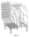
- FIG. 1 there is shown a perspective view of an electrical connector 10 incorporating features of the present invention.
- an electrical connector 10 incorporating features of the present invention.
- the present invention will be described with reference to the embodiments shown in the drawings, it should be understood that the present invention can be embodied in many alternate forms of embodiments.
- any suitable size, shape or type of elements or materials could be used.
- the connector 10 in this embodiment is a receptacle electrical connector adapted to be connected to a first electrical component (not shown) such as a printed circuit board and removably connectable to a mating electrical connector, such as a pin header (see Figure 4).
- the connector 10 and connection system is similar to that described in U.S. provisional patent application No.: 60/117,957 filed January 28, 1999 which is hereby incorporated by reference in its entirety.
- the connector 10 generally comprises a housing 12 and modules or subassembly wafers 14. However, in alternate embodiments more or less components can be provided.
- the housing 12 generally comprises a rear housing member 16 and a front housing member 18.
- rear housing member 16 is generally an open structure formed by sidewalls 35, 37; a rear wall 39; and a top wall 41.
- the open interior of rear housing member 16 receives the rear portions of a series of the modules 14 arranged side-by-side. Specifically a groove 71b receives a spline 71a to ensure proper alignment.
- Receptacle 10 accurately rests on a daughterboard (not shown) using alignment posts 43 extending downwardly from sidewalls 35, 37. Alignment posts 43 engage corresponding through holes in the daughterboard preferably by an interference fit.
- Front housing member 18 is also generally an open structure formed by a mating face 45; sidewalls 47, 49; bottom wall 51; and top wall 53.
- the open interior of The front housing member 18 receives the front portions of the series of modules 14 arranged side-by-side.
- housing 18 can have grooves (not shown) to receive another spline 71a on wafer 30.
- Front housing member 18 secures to rear housing member 16 using latch structures 55, 57 on each housing, respectively.
- the front housing member 18 secures to the rear housing member 16 after placement of the modules 14 within the rear housing member 16. Once assembled, receptacle 10 can mount to the daughterboard.
- the mating face 45 of the front housing member 18 includes an array of lead-ins 59.
- Lead-ins 59 accept corresponding signal pins and ground pins from the header (See Figure 4). Once the header mates with the receptacle 10, the signal and ground contacts of receptacle 10 engage the signal pins and ground pins of the header. This feature will be described in more detail below.
- the connector 10 can include a ground plane member 20.
- the ground plane member 20 is a one-piece member comprised of electrically conductive material which is also ferromagnetic. In alternate embodiments the ground plane member 20 could be comprised of multiple members.
- the ground plane member 20 comprises first connection ends 22 and second connection ends 24.
- the first connection ends 22 comprise through-hole solder trails, but any suitable second connection ends could be provided.
- the second connection ends 24 comprise opposing spring contact arms forming a pin receiving area therebetween, but any suitable second connection ends could be provided.
- the ground plane member 20 has break-off sections 26 between the second connection ends 24 and the main body 28.
- break-off sections can be severed or cut during manufacturing to remove one or more of the second connection ends 24 to customize or configure the ground place member as further understood below.
- the break-off section needs not be provided or any suitable type of severing system could be provided.
- Each module 14 generally comprises a frame or wafer 30, signal contacts 32 and ground contacts 34.
- Wafer 30 can be a block of insulative material.
- the wafer 30 can be formed from several pieces 30a, 30b. Alternatively, however, wafer 30 could be formed unitarily from one piece (not shown).
- the module 14 comprises six'signal contacts and seven ground contacts, but any suitable number of contacts could be provided.
- the center ground contact 34a may also be omitted as further understood below.
- a first major surface 67 of wafer piece 30a has a series of channels, grooves or apertures 68 in which ground contacts 34 reside.
- first major surface 67 of a first module 14 can abut a second major surface 69 of a second adjacent module.
- second major surface 69 can be generally featureless.
- the top surface of wafer piece 30a includes a projection 71. As seen in Figure 1, projections 71 can abut the front edged of rear housing member 16 during, and after, assembly. The interaction between projections 71 and the front edge of rear housing member 16 helps align modules 14 within rear housing member 16.
- the wafer piece 30a can also have a spine 71a.
- the spine 71a can be located in a groove 71b in the rear housing piece 16.
- Signal contacts 32 include a mounting end 73 for securing to the daughterboard, a mating end 75 for interacting with signal pins of the header, and an intermediate portion 77.
- the mounting ends 73 can have press-fit solder tails that engage plated through holes in the daughterboard. However, other types of terminations for mounting ends 73 could be used.
- an overmolding process embeds signal contact 32 in wafer piece 30a (or wafer 30 if one piece), however, other techniques could be used.
- the second wafer piece 30b is preferably premolded and subsequently mounted over the mating ends 75 of the signal contacts 32.
- the second wafer piece 30b includes first receiving apertures 40 and second receiving apertures 42.
- the first receiving apertures 40 receive the mating ends 75 of the signal contacts 32.
- the second receiving apertures 42 receive the mating ends of the ground contacts 34.
- the center second receiving aperture 42a extends into an opposite side of the second wafer piece 30b than the other second receiving apertures 42, but this need not be provided.
- the receiving apertures 40, 42 above the center second receiving aperture 42a are preferably mirror images of the receiving apertures 40,42 below the center second receiving aperture 42a. However, this need not be provided.
- the mating end of the signal contacts 32 can have a dual beam contact configuration to engage signal pins of the header.
- the beams 79, 81 of the dual beam contact are arranged generally perpendicular to each other. In this arrangement, the bifurcation engages adjacent surfaces of the mating signal pins. Beams 79, 81 deflect upon insertion of the mating signal pins. The movement of signal pins along the beams 79, 81 during insertion provides good wiping action. In addition, the force imparted to the signal pins by deflection of the beams 79, 81 provides good contact pressure or contact normal force.
- the ground contacts 34 include a mounting end 83 for securing to the daughterboard, a mating end 85 for interacting with ground pins of the mating header, and an intermediate portion 87.
- Mounting ends 83 can have press-fit solder tails that engage plated through holes in the daughterboard. However, other types of terminations for mounting ends 83 could be used.
- Mating end 85 uses a dual beam-type contact arrangement to engage ground pins of the header.
- Mating end 85 includes a first beam 89 arranged generally perpendicular to a second beam 91. A minor surface of first beam 89 supports the ground pin. As discussed above, the beam 89 provides good contact force and wipe.
- Second beam 91 is bifurcated into a stationary section 93 and movable section 95. Upon engagement of movable section 95 of second beam 91 with a ground pin, movable section 95 deflects. As with the other contacts, the deflection provides good contact force and wipe.
- Signal contacts 32 within module 14, as with ground contacts 34 within module 14, preferably do not maintain the same orientation throughout the module 14. Furthermore, signal contacts 32 and ground contacts 34 in one module 14 preferably do not exhibit the same orientation as signal contacts 32 and ground contacts 34 in all of the other modules 14.
- the connector 10 comprises six of the modules 14. In alternate embodiments more or less than six modules could be used. In this embodiment the six modules 14 actually comprise two types of modules 14a, 14b which are mirror images of each other. In alternate embodiments more or less than two types of modules could be provided and, the modules need not be mirror images of each other.
- the general L shape of the signal contacts 32 generally correspond to the positions of the beams 79, 81.
- the general L shape of the ground contacts 34 generally correspond to the positions of the beams 89, 91.
- Each signal contact 32 corresponds to a ground contact 34 to form a contact pair.
- the signal contact 32 and ground contact 34 in each contact pair have the same orientation.
- signal contact 32 and ground contact 34 of contact pair face the same direction.
- the orientation of each contact pair within a quadrant remains the same.
- contact pairs in other quadrants differ from the orientation of contact pairs in other quadrants (even on the same module).
- contact pairs in one quadrant are rotated 90° relative to contact pairs in an adjacent quadrant.
- a contact pair in quadrant Q1 is rotated 90° relative to a contact pair in quadrant Q2.
- one module 14 can have contacts 32, 34 residing in more than one quadrant, the orientation of some contacts 32, 34 in each module 14 can differ from the orientation of other contacts in the same module.
- contact pairs in a module 14 that reside in one quadrant are preferably mirror images of the contact pairs in the same module that reside in the other quadrant.
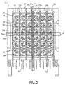
- module 14a in Figure 3 has contact pairs in quadrants Q1 and Q4.
- Contact pairs in module 14a that are in quadrant Q1 are mirror images of the contact pairs in quadrant Q4.
- Other arrangements are also possible. In an appropriate situation, the contact in one quadrant could be rotated 90° to the contacts in the adjacent quadrant.
- Area L1 is generally occupied by the ground plane member 20 for single ended applications.
- the ground plane member 20 forms a ground and a shield through the center of the connector 10 between the signal contacts 32 in the two modules 14a, 14b closest to the ground plane member.
- the top second connection end 24a is located between the mating ends 75a, 75a of the two top signal contacts 32 on opposite sides of the ground plane member.
- Area L2 is generally occupied by the module ground contacts 34a for single ended applications.
- the module ground contacts 34a form both grounds and shields in a path generally through the center of the connector 10 between the signal contacts in each respective module 14 closets to the module ground conl ct 34a.
- the mating ends 75b, 75b of the two middle signal contacts 32 on opposite sides of each module ground contact 34a and their intermediate portions 77 will have the module ground contacts 34a therebetween.
- the ground contacts 34a and ground plane member 20 form a general cross-shaped ground and shield between the four quadrants Q1, Q2, Q3, Q4, but which still allows for 90° offset connection possibilities with the mating electrical connector pin header.
- Ground plane 20, ground contacts 34a and ground contacts 34 form a pseudo-coaxial structure around each signal contact 32.
- the signal contacts 32 are preferably single ended signal contacts.
- FIG. 4 is a front elevational view of a mating electrical connector or header 100 adapted to be connected to the receptacle connector 10.
- the connector 100 is a pin header connector which is fixedly connectable to an electrical component, such as a printed circuit board.
- the connector 100 includes a housing 102, ground contacts 104, associated signal contacts 106, and ground shields 108.
- the housing 102 includes a receiving area 110 for receiving the mating face 45 of the receptacle connector 10.
- the ground contacts 104 have male pin sections 112.
- the signal contacts 106 have male pin sections 114. When the two connectors 10,100 are properly connected to each other, the pin section 112, 114 extend into the lead-ins 59 and make electrical contact with the ground contacts 34 and signal contacts 32, respectively.
- the mating connector 100 may also comprise additional ground contacts 104a.
- the additional ground contacts 104a do not have associated or paired respective signal contacts as the other ground contacts 104 but help create a pseudo-coaxial structure.
- the additional ground contacts 104a are arranged in a general cross-shaped pattern as illustrated by area L3.
- the male pin sections of the additional ground contacts 104a are adapted to make electrical contact with the ground contacts 34a in area L2 and ground plane member 20 in area L1 shown in Figure 3.
- other types of suitable mating connection and/or contacts could be provided.
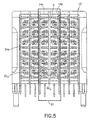
- Figure 5 similar to Figure 3, shows the receptacle connector 10' with its front housing member removed.
- the connector 10' is substantially identical to the connector 10, but does not include the ground plane member 20.
- a shield is not provided between the signal contacts 32 in the two modules 14a, 14b closest to each other at the center of the connector 10'.
- Area A is empty, allowing signal contacts 32 in modules 14a,b to be driven as differential pairs.
- the connector 10' can comprise both single ended signal contacts 32s as well as differential pair signal contacts 32D. More specifically, area B1 forms six differential pair signal contacts; each pair comprising one signal contact from each of the two closest modules 14a, 14b.
- the rest of the signal contacts can remain single ended signal contacts because of the shielding provided by the ground contacts 34, 34a.
- the ground contacts 34, 34a in area B1 also prevent signal interference between adjacent pairs of the differential pair signal contacts 32 D and also between the differential pairs 32 D and the single ended contacts 32 s .
- Figure 6 shows a mating connector 100' similar to the mating connector 100 shown in Figure 4 for use with the connector 10'. As can be seen, the center column of additional ground contacts has been omitted.
- area B2 is formed which can use the six pairs of signal contacts 114 D as differential pair signal contacts.
- the remaining signal contacts 114 s outside area B2 can be used as single ended signal contacts because of the ground shields 108 and ground contacts 104, 104a.
- a ground plane member similar to member 20 could be located in area A, but have all of its second connection ends 24 removed.
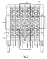
- the receptacle connector 10" is substantially the same as the receptacle connector 10' shown in Figure 5 except that the connector 10" has all the center ground contacts 34a omitted.
- area C1 is formed which comprises ten differential pair signal contacts 114 D .
- Area C1 has a general cross-shape, but any suitable shape could be provided depending upon which ones of the center ground contacts 34a and/or second connection ends 24 are omitted.
- the signal contacts 114 s outside area C1 can be used as single ended signal contacts because of the shielding provided by the ground contacts 34.
- a mating connector 100" is shown similar to the mating connector 100' shown in Figure 6 for use with the connector 10".
- area C2 is formed which can use the ten pairs of signal contacts.
- the remaining signal contacts 114D i.e. those not used as differential pair signal contacts
- outside area C2 can be used as single ended signal contacts 114s because of the ground shields 108 and ground contacts 104.
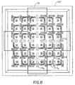
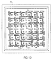
- Figures 9-12 show other alternate embodiments of the mating connectors, it being understood that their respective receptacle connectors would be correspondingly configured to mate similar to the connectors 10 and 100, 10' and 100', and 10" and 100".
- the receptacle connectors would have the appropriate second connection ends 24 of the ground plane member 20 removed and/or the appropriate center ground members 34a omitted corresponding to the empty apertures 29 in the housing of the mating connector.
- the mating connector 200 is similar to the mating connector 10 shown in Figure 4, but has four empty apertures 29. This forms an area D2 having differential pair signal contacts 114 D .
- the contacts 114 s outside the area D2 can be used as single ended signal contacts due to the shielding provided by ground shields 108 and ground contacts 104, 104a.
- the mating connector 202 is similar to the mating connector 10 shown in Figure 4, but has eight empty apertures 29. This forms an area E2 having differential pair signal contacts 114 D .
- the contacts 114 S outside the area E2 can be used as single ended signal contacts due to the shielding provided by ground shields 108 and ground contacts 104, 104a.
- the mating connector 204 is similar to the mating connector 10 shown in Figure 4, but has nine empty apertures 29. This forms an area F2 with a general "T" Shape having differential pair signal contacts 114 D .
- the contacts 114 s outside the area F2 can be used as single ended signal contacts due to the shielding provided by ground shields 108 and ground contacts 104, 104a.
- This embodiment also illustrates that the patterns for the differential pair signal contacts and single ended signal contacts can be asymmetric. In such an asymmetric arrangement, the mating connectors should mate in only one orientation.
- the mating connector 206 is similar to the mating connector 10 shown in Figure 4, but has four empty apertures 29 provided as two spaced apart groups. This forms two areas G2 a , G2 b having differential pair signal contacts 114 D .
- the contacts 114 S outside the areas G2 a , G2 b can be used as single ended signal contacts due to the shielding provided by ground shields 108 and ground contacts 104, 104a.
- This embodiment illustrates that the differential pair contacts can be provided as more than one group or area (perhaps spaced from each other) and do not need to pass through the center of the connector.
- the connector 208 includes an array of 8x8 signal contacts.
- the ground contact layout and ground shields are not shown merely for the sake of clarity. This arrangement is achieved by allowing the placement of ground plane 20 at locations other than a central position.
- the connector 208 includes three groups (H2 a , H2 b , H2 c ) which are separated by two groups of single ended signal contacts 114 s .
- ground planes 20 are place between: (1) group H2 a and the row of single ended contacts, 114 s ; (2) the row of single ended contacts 114 s and group H2 b .
- the layout or pattern for the signal contacts could be varied such as not having any signal ended signal contacts, having only one group of single ended signal contacts, having more than three groups of differential pair signal contacts (spaced from each other and/or not spaced from each other), and having symmetric and/or non-symmetric patterns.
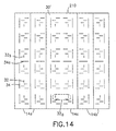
- the connector 210 comprises five modules or wafer subassemblies 14a, 14b and 14c.
- the modules form a 6x6 array of paired signal and ground contracts 32, 34 as well as additional ground contacts 34a.
- the connector only has two left-hand modules 14a and two right hand modules 14b.
- the left and right hand modules 14a, 14b each comprise a 1x6 array of only single ended signal contacts 32s.
- the left and right hand modules 14a, 14b could also form differential pair signal contacts.
- the center module 14c comprises a 2x6 array of associated signal and ground contacts in a common wafer housing 30' forming six differential pair signal contacts 32D.
- the single module 14c comprises differential pair signal contacts in a common housing.
- the center module 14c could include single ended signal contacts, such as when the housing 30' is adapted to receive a ground plane member.
Landscapes
- Details Of Connecting Devices For Male And Female Coupling (AREA)
- Coupling Device And Connection With Printed Circuit (AREA)
- Multi-Conductor Connections (AREA)
- Manufacturing Of Electrical Connectors (AREA)
- Connector Housings Or Holding Contact Members (AREA)
Abstract
Description
Claims (28)
- An electrical connector (10) comprising:a housing (12); andelectrical contacts connected to the housing (12), the electrical contacts comprising paired signal and ground contacts (32, 34), and additional ground contacts (34a),wherein the additional ground contacts (34a) are arranged relative to the paired contacts (32, 34) to divide the paired contacts into subdivisions of equal numbers of the paired contacts.
- An electrical connector (10) as in Claim 1 wherein the subdivisions comprise four quadrants (Q1 - Q4).
- An electrical connector (10) as in Claim 1 wherein the additional ground contacts (34a) form a general cross shape.
- An electrical connector (10) as in Claim 1 wherein a portion of the housing (12), the paired contacts (32, 34), and some of the additional ground contacts (34a) are formed as subassembly wafers (14) which are subsequently sandwiched together to form the electrical connector (10).
- An electrical connector (10) as in Claim 4 wherein the additional ground contacts (34a) include at least one of the additional ground contacts (34a) being sandwiched between two of the subassembly wafers (14).
- An electrical connector (10) as in Claim 1 wherein the additional ground contacts (34a) comprise a row (L2) of horizontally centered and a column (L1) of vertically centered connection areas at a mating connector connection area.
- An electrical connector (10) as in Claim 1 wherein the subdivisions and the additional ground contacts (34a) are arranged to allow for multiple relative orientation connections of a mating connector.
- An electrical connector comprising:subassembly wafers (14), at least two of the wafers comprising a housing (12), paired signal and ground contacts (32, 34), and an additional ground contact (34a) in a general center of a connection area for the paired contacts; anda ground plane member (20) located between at least two of the wafers (14), the ground plane member (20) having contact areas (24) located between at least some of the paired contacts (32, 34) of one of the at least two wafers (14) and at least some of the paired contacts (32, 34) of the other one of the at least two wafers (14).
- An electrical connector (10) as in Claim 8, wherein the at least two wafers (14) each have equal numbers of paired contacts (32, 34) on opposite sides of their respective additional ground contact (34a).
- An electrical connector (10) as in Claim 8 wherein the ground plane member (20) has contact areas (24) located between all the paired contacts (32, 34) of the one wafer and the other wafer.
- An electrical connector (10) as in Claim 8 wherein the additional ground contacts (34a) and the ground plane member (20) form a general cross shape at the connection area.
- An electrical connector (10) as in Claim 11 wherein the general cross shape divides the paired contacts into four quadrants (Q1 - Q4) of equal numbers of the paired contacts (32, 34).
- An electrical connector (10) as in Claim 8 wherein first paired contacts of the one wafer and second paired contacts of the other wafer do not have a contact area (24) of the ground plane member (20) therebetween such that the signal contacts (32) of the first and second contacts form high speed differential pair signal transmission contacts.
- An electrical connector (10) comprising:paired signal and ground contacts (32, 34);additional ground contacts (34a) located between at least some of the paired contacts (32, 34); anda housing (12) having first contact receiving areas (45) with the paired contacts (32, 34) located therein and second contact receiving areas (24) with the additional ground contacts (34a) located therein, wherein at least one of the second contact receiving areas (24) does not contain an additional ground contact (34a) such that two of the paired contacts (32, 34) on opposite sides of the at least one second contact receiving area (24) form a differential pair of contacts for high speed differential pair signal transmission.
- An electrical connector (10) as in Claim 14 wherein the at least one second contact receiving area (24) comprises one of the second contact receiving areas located in a center vertical column of the second contact receiving areas (24).
- An electrical connector (10) as in Claim 15 wherein the at least one second contact receiving area (24) comprises all of the receiving areas in the center vertical column of second contact receiving areas.
- An electrical connector (10) as in Claim 15 wherein the at least one second contact receiving areas (24) comprises one of the second contact receiving areas located in a center horizontal row of the second contact receiving areas.
- An electrical connector (10) as in Claim 17 wherein the at least one second contact receiving area (24) comprises all of the receiving areas in the horizontal row of second contact receiving areas.
- An electrical connector (10) as in Claim 14 wherein the paired contacts (32, 34) located on opposite sides of one of the second contact receiving areas (24) having an additional ground contact (34a) therein form individual single ended signal transmission contacts.
- An electrical connector (10) as in Claim 19 wherein the contacts have mating ends (75) located at a mating area for connection to a mating connector (100), wherein the electrical connector (10) comprises a plurality of the differential pair of contacts (32, 34), and wherein the mating ends (75) of the plurality of differential pair of contacts (32, 34) are arranged in a symmetrical pattern at the mating area.
- An electrical connector (10) as in Claim 19 wherein the contacts (32, 34) have mating ends (75) located at a mating area for connection to a mating connector (100), wherein the electrical connector (10) comprises a plurality of the differential pair of contacts (32, 34), and wherein the mating ends (75) of the plurality of differential pair of contacts are arranged in a non-symmetrical pattern at the mating area.
- A method of manufacturing an electrical connector (10) comprising steps of:providing a housing (12) having first contact receiving areas (45) and second contact receiving areas (24),positioning paired signal and ground contacts (32, 34) in the first contact receiving areas (45); andselectively positioning additional ground contacts (34a) in the second contact receiving areas (24),wherein at least one of the second contact receiving areas (24) does not have an additional ground contact (34a) located therein such that two of the paired signal contacts (32) each on opposite sides of the at least one second contact receiving area (24), form a differential pair of high speed signal transmission contacts.
- A method as in Claim 22 wherein the second contact receiving areas (24) include a center row, and wherein equal numbers of the paired contacts (32, 34) are positioned on opposite sides of the center row.
- A method as in Claim 23 wherein the second contact receiving areas (24) include a center column, and equal numbers of the paired contacts (32, 34) are positioned on opposite sides of the center column.
- A method as in Claim 22 wherein the step of providing a housing (12) comprises providing multiple wafer housings (14) and connecting the wafer housings (14) to each other in series.
- A method as in Claim 25 wherein the step of positioning additional ground contacts (34a) comprises locating a ground plane member (20) between two of the wafer housings (14).
- An electrical connector (10) comprising:a first subcomponent wafer assembly (14) comprising a first housing (12) and single ended signal and respectively paired ground contacts (32, 34) connected to the first housing (12); anda second subcomponent wafer assembly (14) connected to the first subcomponent wafer assembly (14), the second subcomponent wafer assembly comprising a second housing and, connected to the second housing, pairs of differential pair signal contacts (32) and respectively associated ground contacts (34) for each signal contact.
- A method of manufacturing electrical connectors (10) having both single ended signal contacts and differential pair signal contacts comprising steps of:providing at least two first pairs of signal contacts (32) and respective ground contacts (34) for each of the first pairs of signal contacts;providing at least two second pairs of signal contacts (32) and respective ground contacts for each of the second pairs of signal contacts; andselectively locating additional ground contacts (34a) between two of the first pairs of signal contacts (32),wherein at least two of the second pairs of signal contacts (32) do not have the additional ground contacts (34a) therebetween such that the signal contacts (32) of the two second pairs form a differential pair of high speed signal transmission signal contacts and signal contacts (32) of the two first pairs form single ended signal transmission signal contacts.
Priority Applications (1)
| Application Number | Priority Date | Filing Date | Title |
|---|---|---|---|
| EP03025660A EP1394907B1 (en) | 2000-03-29 | 2001-03-27 | Electrical connector with grounding system and method of manufacturing the same |
Applications Claiming Priority (2)
| Application Number | Priority Date | Filing Date | Title |
|---|---|---|---|
| US537502 | 2000-03-29 | ||
| US09/537,502 US6364710B1 (en) | 2000-03-29 | 2000-03-29 | Electrical connector with grounding system |
Related Child Applications (1)
| Application Number | Title | Priority Date | Filing Date |
|---|---|---|---|
| EP03025660A Division EP1394907B1 (en) | 2000-03-29 | 2001-03-27 | Electrical connector with grounding system and method of manufacturing the same |
Publications (3)
| Publication Number | Publication Date |
|---|---|
| EP1139498A2 true EP1139498A2 (en) | 2001-10-04 |
| EP1139498A3 EP1139498A3 (en) | 2002-04-03 |
| EP1139498B1 EP1139498B1 (en) | 2004-08-18 |
Family
ID=24142911
Family Applications (2)
| Application Number | Title | Priority Date | Filing Date |
|---|---|---|---|
| EP03025660A Expired - Lifetime EP1394907B1 (en) | 2000-03-29 | 2001-03-27 | Electrical connector with grounding system and method of manufacturing the same |
| EP01107457A Expired - Lifetime EP1139498B1 (en) | 2000-03-29 | 2001-03-27 | Electrical connector with grounding system |
Family Applications Before (1)
| Application Number | Title | Priority Date | Filing Date |
|---|---|---|---|
| EP03025660A Expired - Lifetime EP1394907B1 (en) | 2000-03-29 | 2001-03-27 | Electrical connector with grounding system and method of manufacturing the same |
Country Status (7)
| Country | Link |
|---|---|
| US (2) | US6364710B1 (en) |
| EP (2) | EP1394907B1 (en) |
| JP (1) | JP2001307817A (en) |
| KR (1) | KR100721893B1 (en) |
| AT (2) | ATE363751T1 (en) |
| CA (1) | CA2342008A1 (en) |
| DE (2) | DE60104928T2 (en) |
Cited By (7)
| Publication number | Priority date | Publication date | Assignee | Title |
|---|---|---|---|---|
| EP1311038A3 (en) * | 2001-11-12 | 2004-09-15 | Fci | Connector for high-speed communications |
| US7549897B2 (en) | 2006-08-02 | 2009-06-23 | Tyco Electronics Corporation | Electrical connector having improved terminal configuration |
| US7591655B2 (en) | 2006-08-02 | 2009-09-22 | Tyco Electronics Corporation | Electrical connector having improved electrical characteristics |
| US7670196B2 (en) | 2006-08-02 | 2010-03-02 | Tyco Electronics Corporation | Electrical terminal having tactile feedback tip and electrical connector for use therewith |
| US7753742B2 (en) | 2006-08-02 | 2010-07-13 | Tyco Electronics Corporation | Electrical terminal having improved insertion characteristics and electrical connector for use therewith |
| US8142236B2 (en) | 2006-08-02 | 2012-03-27 | Tyco Electronics Corporation | Electrical connector having improved density and routing characteristics and related methods |
| EP2980927A1 (en) * | 2014-07-29 | 2016-02-03 | Tyco Electronics Corporation | High speed signal-isolating electrical connector assembly |
Families Citing this family (99)
| Publication number | Priority date | Publication date | Assignee | Title |
|---|---|---|---|---|
| HU224993B1 (en) * | 1999-01-28 | 2006-05-29 | Framatome Connectors Int | Connector system and electrical connector |
| DE19938782A1 (en) * | 1999-08-16 | 2001-03-22 | Tyco Electronics Logistics Ag | Shielded electrical connector |
| US6623302B2 (en) * | 2000-12-21 | 2003-09-23 | Hon Hai Precision Ind. Co., Ltd. | Electrical connector having printed substrates therein electrically contacting conductive contacts thereof by solderless |
| US6979202B2 (en) | 2001-01-12 | 2005-12-27 | Litton Systems, Inc. | High-speed electrical connector |
| US6910897B2 (en) | 2001-01-12 | 2005-06-28 | Litton Systems, Inc. | Interconnection system |
| US6843657B2 (en) * | 2001-01-12 | 2005-01-18 | Litton Systems Inc. | High speed, high density interconnect system for differential and single-ended transmission applications |
| US6409543B1 (en) * | 2001-01-25 | 2002-06-25 | Teradyne, Inc. | Connector molding method and shielded waferized connector made therefrom |
| US6551140B2 (en) * | 2001-05-09 | 2003-04-22 | Hon Hai Precision Ind. Co., Ltd. | Electrical connector having differential pair terminals with equal length |
| US6869292B2 (en) * | 2001-07-31 | 2005-03-22 | Fci Americas Technology, Inc. | Modular mezzanine connector |
| US20050196987A1 (en) * | 2001-11-14 | 2005-09-08 | Shuey Joseph B. | High density, low noise, high speed mezzanine connector |
| US20050170700A1 (en) * | 2001-11-14 | 2005-08-04 | Shuey Joseph B. | High speed electrical connector without ground contacts |
| US6994569B2 (en) * | 2001-11-14 | 2006-02-07 | Fci America Technology, Inc. | Electrical connectors having contacts that may be selectively designated as either signal or ground contacts |
| US7390200B2 (en) * | 2001-11-14 | 2008-06-24 | Fci Americas Technology, Inc. | High speed differential transmission structures without grounds |
| US6981883B2 (en) * | 2001-11-14 | 2006-01-03 | Fci Americas Technology, Inc. | Impedance control in electrical connectors |
| US6976886B2 (en) * | 2001-11-14 | 2005-12-20 | Fci Americas Technology, Inc. | Cross talk reduction and impedance-matching for high speed electrical connectors |
| US6979215B2 (en) * | 2001-11-28 | 2005-12-27 | Molex Incorporated | High-density connector assembly with flexural capabilities |
| US6488520B1 (en) * | 2001-12-27 | 2002-12-03 | Fci Americas Technology, Inc. | Electrical connector assembly with shorting members |
| US6899566B2 (en) | 2002-01-28 | 2005-05-31 | Erni Elektroapparate Gmbh | Connector assembly interface for L-shaped ground shields and differential contact pairs |
| US6739918B2 (en) * | 2002-02-01 | 2004-05-25 | Teradyne, Inc. | Self-aligning electrical connector |
| US6655966B2 (en) | 2002-03-19 | 2003-12-02 | Tyco Electronics Corporation | Modular connector with grounding interconnect |
| JP2006515705A (en) | 2002-05-06 | 2006-06-01 | モレックス インコーポレーテッド | Differential signal connector with electrostatic discharge protection function |
| US6638079B1 (en) * | 2002-05-21 | 2003-10-28 | Hon Hai Precision Ind. Co., Ltd. | Customizable electrical connector |
| US6634908B1 (en) * | 2002-05-30 | 2003-10-21 | Hon Hai Precision Ind. Co., Ltd. | High density electrical connector with improved grounding bus |
| JP2004087348A (en) * | 2002-08-28 | 2004-03-18 | Fujitsu Component Ltd | Connector device |
| US6695646B1 (en) * | 2002-10-18 | 2004-02-24 | Hon Hai Precision Ind. Co., Ltd. | Electrical connector having floatable chicklets |
| WO2004051809A2 (en) * | 2002-12-04 | 2004-06-17 | Molex Incorporated | High-density connector assembly with tracking ground structure |
| JP3841348B2 (en) * | 2003-02-25 | 2006-11-01 | 日本航空電子工業株式会社 | Connector ground structure |
| US6843687B2 (en) * | 2003-02-27 | 2005-01-18 | Molex Incorporated | Pseudo-coaxial wafer assembly for connector |
| US6814619B1 (en) * | 2003-06-26 | 2004-11-09 | Teradyne, Inc. | High speed, high density electrical connector and connector assembly |
| US6776659B1 (en) * | 2003-06-26 | 2004-08-17 | Teradyne, Inc. | High speed, high density electrical connector |
| US7083432B2 (en) * | 2003-08-06 | 2006-08-01 | Fci Americas Technology, Inc. | Retention member for connector system |
| US6884117B2 (en) * | 2003-08-29 | 2005-04-26 | Hon Hai Precision Ind. Co., Ltd. | Electrical connector having circuit board modules positioned between metal stiffener and a housing |
| US7074086B2 (en) * | 2003-09-03 | 2006-07-11 | Amphenol Corporation | High speed, high density electrical connector |
| US7517250B2 (en) | 2003-09-26 | 2009-04-14 | Fci Americas Technology, Inc. | Impedance mating interface for electrical connectors |
| US7524209B2 (en) | 2003-09-26 | 2009-04-28 | Fci Americas Technology, Inc. | Impedance mating interface for electrical connectors |
| JP3909769B2 (en) * | 2004-01-09 | 2007-04-25 | 日本航空電子工業株式会社 | connector |
| NL1027045C2 (en) * | 2004-09-15 | 2006-03-16 | Framatome Connectors Int | Connector provided with a shield plate. |
| US7281950B2 (en) * | 2004-09-29 | 2007-10-16 | Fci Americas Technology, Inc. | High speed connectors that minimize signal skew and crosstalk |
| US7267585B2 (en) * | 2005-03-24 | 2007-09-11 | International Business Machines Corporation | Method and system for easing attachment of a peripheral cable to a personal computer |
| US20060228912A1 (en) * | 2005-04-07 | 2006-10-12 | Fci Americas Technology, Inc. | Orthogonal backplane connector |
| US20060245137A1 (en) * | 2005-04-29 | 2006-11-02 | Fci Americas Technology, Inc. | Backplane connectors |
| US20090291593A1 (en) | 2005-06-30 | 2009-11-26 | Prescott Atkinson | High frequency broadside-coupled electrical connector |
| DE202005020474U1 (en) * | 2005-12-31 | 2006-02-23 | Erni Elektroapparate Gmbh | Connectors |
| JP4958183B2 (en) * | 2006-01-20 | 2012-06-20 | タイコ エレクトロニクス ネーデルランド ビーヴイ | Electrical connector |
| US7462924B2 (en) * | 2006-06-27 | 2008-12-09 | Fci Americas Technology, Inc. | Electrical connector with elongated ground contacts |
| US7500871B2 (en) * | 2006-08-21 | 2009-03-10 | Fci Americas Technology, Inc. | Electrical connector system with jogged contact tails |
| US7713088B2 (en) | 2006-10-05 | 2010-05-11 | Fci | Broadside-coupled signal pair configurations for electrical connectors |
| USD578486S1 (en) * | 2006-10-19 | 2008-10-14 | Mitsubishi Cable Industries Ltd. | Electric connector housing |
| USD578485S1 (en) * | 2006-10-19 | 2008-10-14 | Mitsubishi Cable Industries Ltd. | Electric connector housing |
| US7708569B2 (en) | 2006-10-30 | 2010-05-04 | Fci Americas Technology, Inc. | Broadside-coupled signal pair configurations for electrical connectors |
| US7497736B2 (en) | 2006-12-19 | 2009-03-03 | Fci Americas Technology, Inc. | Shieldless, high-speed, low-cross-talk electrical connector |
| CN101689738B (en) * | 2007-05-23 | 2013-02-27 | Fci公司 | Electrical connector with interleaved single-ended contacts |
| US7811100B2 (en) * | 2007-07-13 | 2010-10-12 | Fci Americas Technology, Inc. | Electrical connector system having a continuous ground at the mating interface thereof |
| US7666009B2 (en) * | 2008-02-08 | 2010-02-23 | Fci Americas Technology, Inc. | Shared hole orthogonal footprints |
| US8764464B2 (en) | 2008-02-29 | 2014-07-01 | Fci Americas Technology Llc | Cross talk reduction for high speed electrical connectors |
| US7674133B2 (en) * | 2008-06-11 | 2010-03-09 | Tyco Electronics Corporation | Electrical connector with ground contact modules |
| WO2010030622A1 (en) * | 2008-09-09 | 2010-03-18 | Molex Incorporated | Connector with impedance tuned terminal arrangement |
| US8545240B2 (en) | 2008-11-14 | 2013-10-01 | Molex Incorporated | Connector with terminals forming differential pairs |
| MY155071A (en) | 2008-12-12 | 2015-08-28 | Molex Inc | Resonance modifying connector |
| US9277649B2 (en) | 2009-02-26 | 2016-03-01 | Fci Americas Technology Llc | Cross talk reduction for high-speed electrical connectors |
| CN201374417Y (en) * | 2009-03-02 | 2009-12-30 | 富士康(昆山)电脑接插件有限公司 | backplane connector |
| US8366485B2 (en) | 2009-03-19 | 2013-02-05 | Fci Americas Technology Llc | Electrical connector having ribbed ground plate |
| US8231415B2 (en) | 2009-07-10 | 2012-07-31 | Fci Americas Technology Llc | High speed backplane connector with impedance modification and skew correction |
| JP2011018621A (en) * | 2009-07-10 | 2011-01-27 | Fujitsu Component Ltd | Connector component and connector |
| US8608510B2 (en) * | 2009-07-24 | 2013-12-17 | Fci Americas Technology Llc | Dual impedance electrical connector |
| US8267721B2 (en) | 2009-10-28 | 2012-09-18 | Fci Americas Technology Llc | Electrical connector having ground plates and ground coupling bar |
| US8616919B2 (en) | 2009-11-13 | 2013-12-31 | Fci Americas Technology Llc | Attachment system for electrical connector |
| SG181953A1 (en) * | 2009-12-30 | 2012-07-30 | Framatome Connectors Int | Electrical connector having impedence tuning ribs |
| WO2011140438A2 (en) | 2010-05-07 | 2011-11-10 | Amphenol Corporation | High performance cable connector |
| US9136634B2 (en) | 2010-09-03 | 2015-09-15 | Fci Americas Technology Llc | Low-cross-talk electrical connector |
| US8469745B2 (en) * | 2010-11-19 | 2013-06-25 | Tyco Electronics Corporation | Electrical connector system |
| US8657627B2 (en) | 2011-02-02 | 2014-02-25 | Amphenol Corporation | Mezzanine connector |
| US8727809B2 (en) * | 2011-09-06 | 2014-05-20 | Samtec, Inc. | Center conductor with surrounding shield and edge card connector with same |
| EP2624034A1 (en) | 2012-01-31 | 2013-08-07 | Fci | Dismountable optical coupling device |
| USD727268S1 (en) | 2012-04-13 | 2015-04-21 | Fci Americas Technology Llc | Vertical electrical connector |
| US9257778B2 (en) | 2012-04-13 | 2016-02-09 | Fci Americas Technology | High speed electrical connector |
| USD718253S1 (en) | 2012-04-13 | 2014-11-25 | Fci Americas Technology Llc | Electrical cable connector |
| US8944831B2 (en) | 2012-04-13 | 2015-02-03 | Fci Americas Technology Llc | Electrical connector having ribbed ground plate with engagement members |
| USD727852S1 (en) | 2012-04-13 | 2015-04-28 | Fci Americas Technology Llc | Ground shield for a right angle electrical connector |
| US9543703B2 (en) | 2012-07-11 | 2017-01-10 | Fci Americas Technology Llc | Electrical connector with reduced stack height |
| USD751507S1 (en) | 2012-07-11 | 2016-03-15 | Fci Americas Technology Llc | Electrical connector |
| CN104704682B (en) | 2012-08-22 | 2017-03-22 | 安费诺有限公司 | High-frequency electrical connector |
| USD745852S1 (en) | 2013-01-25 | 2015-12-22 | Fci Americas Technology Llc | Electrical connector |
| USD720698S1 (en) | 2013-03-15 | 2015-01-06 | Fci Americas Technology Llc | Electrical cable connector |
| WO2015112717A1 (en) | 2014-01-22 | 2015-07-30 | Amphenol Corporation | High speed, high density electrical connector with shielded signal paths |
| US9401569B2 (en) * | 2014-10-06 | 2016-07-26 | Tyco Electronics Corporation | Electrical connector assembly having signal modules and ground shields |
| US10541482B2 (en) | 2015-07-07 | 2020-01-21 | Amphenol Fci Asia Pte. Ltd. | Electrical connector with cavity between terminals |
| CN105958245B (en) * | 2016-06-08 | 2018-10-12 | 欧品电子(昆山)有限公司 | High speed connector component, socket connector and its female terminal |
| TWI790798B (en) | 2016-08-23 | 2023-01-21 | 美商安芬諾股份有限公司 | Connector configurable for high performance |
| CN208862209U (en) | 2018-09-26 | 2019-05-14 | 安费诺东亚电子科技(深圳)有限公司 | A kind of connector and its pcb board of application |
| TW202439723A (en) | 2019-02-19 | 2024-10-01 | 美商安芬諾股份有限公司 | Electrical connector and method for manufacturing electrical connector |
| TW202607982A (en) | 2020-01-27 | 2026-02-16 | 美商Fci美國有限責任公司 | Electrical connector |
| TW202534957A (en) | 2020-01-27 | 2025-09-01 | 美商Fci美國有限責任公司 | High speed, high density direct mate orthogonal connector |
| CN111430992B (en) * | 2020-03-11 | 2021-11-02 | 上海航天科工电器研究院有限公司 | Lead frame assembly for high-speed electric connector |
| CN215816516U (en) | 2020-09-22 | 2022-02-11 | 安费诺商用电子产品(成都)有限公司 | Electrical connector |
| CN213636403U (en) | 2020-09-25 | 2021-07-06 | 安费诺商用电子产品(成都)有限公司 | Electrical connector |
| CN114765329A (en) * | 2021-01-13 | 2022-07-19 | 泰科电子(上海)有限公司 | Electrical connector, connector assembly and method of manufacturing an electrical connector |
| CN215266741U (en) | 2021-08-13 | 2021-12-21 | 安费诺商用电子产品(成都)有限公司 | High-performance card connector meeting high-bandwidth transmission |
| KR102838731B1 (en) * | 2024-11-08 | 2025-07-29 | (주)메리테크 | Connector for circuit board |
Family Cites Families (18)
| Publication number | Priority date | Publication date | Assignee | Title |
|---|---|---|---|---|
| US4571014A (en) | 1984-05-02 | 1986-02-18 | At&T Bell Laboratories | High frequency modular connector |
| US4824383A (en) | 1986-11-18 | 1989-04-25 | E. I. Du Pont De Nemours And Company | Terminator and corresponding receptacle for multiple electrical conductors |
| US4975084A (en) | 1988-10-17 | 1990-12-04 | Amp Incorporated | Electrical connector system |
| GB8928777D0 (en) * | 1989-12-20 | 1990-02-28 | Amp Holland | Sheilded backplane connector |
| US5197893A (en) * | 1990-03-14 | 1993-03-30 | Burndy Corporation | Connector assembly for printed circuit boards |
| US5046960A (en) | 1990-12-20 | 1991-09-10 | Amp Incorporated | High density connector system |
| US5620340A (en) | 1992-12-31 | 1997-04-15 | Berg Technology, Inc. | Connector with improved shielding |
| NL9300971A (en) | 1993-06-04 | 1995-01-02 | Framatome Connectors Belgium | Circuit board connector assembly. |
| US5304069A (en) | 1993-07-22 | 1994-04-19 | Molex Incorporated | Grounding electrical connectors |
| JPH07122335A (en) * | 1993-10-20 | 1995-05-12 | Minnesota Mining & Mfg Co <3M> | Connector for high-speed transmission |
| DE4446098C2 (en) * | 1994-12-22 | 1998-11-26 | Siemens Ag | Shielded electrical connector |
| US5795191A (en) * | 1996-09-11 | 1998-08-18 | Preputnick; George | Connector assembly with shielded modules and method of making same |
| US6083047A (en) * | 1997-01-16 | 2000-07-04 | Berg Technology, Inc. | Modular electrical PCB assembly connector |
| US6056559A (en) * | 1997-10-01 | 2000-05-02 | Berg Technology, Inc. | Punched sheet coax header |
| US6120306A (en) * | 1997-10-15 | 2000-09-19 | Berg Technology, Inc. | Cast coax header/socket connector system |
| AU9757598A (en) * | 1997-11-19 | 1999-06-07 | Whitaker Corporation, The | Shielded electrical connector |
| JP2000067955A (en) * | 1998-08-17 | 2000-03-03 | Fujitsu Takamisawa Component Ltd | Jack, plug, and connector device |
| US6116926A (en) * | 1999-04-21 | 2000-09-12 | Berg Technology, Inc. | Connector for electrical isolation in a condensed area |
-
2000
- 2000-03-29 US US09/537,502 patent/US6364710B1/en not_active Expired - Lifetime
-
2001
- 2001-03-26 CA CA002342008A patent/CA2342008A1/en not_active Abandoned
- 2001-03-27 AT AT03025660T patent/ATE363751T1/en not_active IP Right Cessation
- 2001-03-27 DE DE60104928T patent/DE60104928T2/en not_active Expired - Lifetime
- 2001-03-27 DE DE60128732T patent/DE60128732T2/en not_active Expired - Lifetime
- 2001-03-27 EP EP03025660A patent/EP1394907B1/en not_active Expired - Lifetime
- 2001-03-27 AT AT01107457T patent/ATE274243T1/en not_active IP Right Cessation
- 2001-03-27 EP EP01107457A patent/EP1139498B1/en not_active Expired - Lifetime
- 2001-03-28 JP JP2001092277A patent/JP2001307817A/en not_active Withdrawn
- 2001-03-29 KR KR1020010016371A patent/KR100721893B1/en not_active Expired - Fee Related
- 2001-07-10 US US09/901,819 patent/US6343955B2/en not_active Expired - Lifetime
Cited By (11)
| Publication number | Priority date | Publication date | Assignee | Title |
|---|---|---|---|---|
| EP1311038A3 (en) * | 2001-11-12 | 2004-09-15 | Fci | Connector for high-speed communications |
| US6848944B2 (en) | 2001-11-12 | 2005-02-01 | Fci Americas Technology, Inc. | Connector for high-speed communications |
| US7310875B2 (en) | 2001-11-12 | 2007-12-25 | Fci Americas Technology, Inc. | Connector for high-speed communications |
| US7549897B2 (en) | 2006-08-02 | 2009-06-23 | Tyco Electronics Corporation | Electrical connector having improved terminal configuration |
| US7591655B2 (en) | 2006-08-02 | 2009-09-22 | Tyco Electronics Corporation | Electrical connector having improved electrical characteristics |
| US7670196B2 (en) | 2006-08-02 | 2010-03-02 | Tyco Electronics Corporation | Electrical terminal having tactile feedback tip and electrical connector for use therewith |
| US7753742B2 (en) | 2006-08-02 | 2010-07-13 | Tyco Electronics Corporation | Electrical terminal having improved insertion characteristics and electrical connector for use therewith |
| US7789716B2 (en) | 2006-08-02 | 2010-09-07 | Tyco Electronics Corporation | Electrical connector having improved terminal configuration |
| US8142236B2 (en) | 2006-08-02 | 2012-03-27 | Tyco Electronics Corporation | Electrical connector having improved density and routing characteristics and related methods |
| EP2980927A1 (en) * | 2014-07-29 | 2016-02-03 | Tyco Electronics Corporation | High speed signal-isolating electrical connector assembly |
| US9559465B2 (en) | 2014-07-29 | 2017-01-31 | Tyco Electronics Corporation | High speed signal-isolating electrical connector assembly |
Also Published As
| Publication number | Publication date |
|---|---|
| KR100721893B1 (en) | 2007-05-28 |
| DE60104928T2 (en) | 2005-08-11 |
| EP1394907A2 (en) | 2004-03-03 |
| KR20010093757A (en) | 2001-10-29 |
| DE60128732T2 (en) | 2008-01-24 |
| JP2001307817A (en) | 2001-11-02 |
| US6364710B1 (en) | 2002-04-02 |
| US6343955B2 (en) | 2002-02-05 |
| US20010041477A1 (en) | 2001-11-15 |
| ATE363751T1 (en) | 2007-06-15 |
| EP1394907B1 (en) | 2007-05-30 |
| EP1139498B1 (en) | 2004-08-18 |
| ATE274243T1 (en) | 2004-09-15 |
| CA2342008A1 (en) | 2001-09-29 |
| DE60104928D1 (en) | 2004-09-23 |
| EP1394907A3 (en) | 2004-03-31 |
| DE60128732D1 (en) | 2007-07-12 |
| EP1139498A3 (en) | 2002-04-03 |
Similar Documents
| Publication | Publication Date | Title |
|---|---|---|
| US6364710B1 (en) | Electrical connector with grounding system | |
| US6607401B1 (en) | Electrical connector mateable in a plurality of orientations | |
| US6979215B2 (en) | High-density connector assembly with flexural capabilities | |
| US6322379B1 (en) | Connector for electrical isolation in a condensed area | |
| CN100524954C (en) | High density connector assembly with leakage grounding structure | |
| WO2003030304A2 (en) | High speed docking connector | |
| WO2012050628A1 (en) | Electrical connector assembly and system | |
| MXPA00000937A (en) | Electrical connector mateable in a plurality of orientations |
Legal Events
| Date | Code | Title | Description |
|---|---|---|---|
| PUAI | Public reference made under article 153(3) epc to a published international application that has entered the european phase |
Free format text: ORIGINAL CODE: 0009012 |
|
| AK | Designated contracting states |
Kind code of ref document: A2 Designated state(s): AT BE CH CY DE DK ES FI FR GB GR IE IT LI LU MC NL PT SE TR |
|
| AX | Request for extension of the european patent |
Free format text: AL;LT;LV;MK;RO;SI |
|
| PUAL | Search report despatched |
Free format text: ORIGINAL CODE: 0009013 |
|
| AK | Designated contracting states |
Kind code of ref document: A3 Designated state(s): AT BE CH CY DE DK ES FI FR GB GR IE IT LI LU MC NL PT SE TR |
|
| AX | Request for extension of the european patent |
Free format text: AL;LT;LV;MK;RO;SI |
|
| RIC1 | Information provided on ipc code assigned before grant |
Free format text: 7H 01R 12/16 A, 7H 01R 23/68 B |
|
| 17P | Request for examination filed |
Effective date: 20020920 |
|
| AKX | Designation fees paid |
Free format text: AT BE CH CY DE DK ES FI FR GB GR IE IT LI LU MC NL PT SE TR |
|
| 17Q | First examination report despatched |
Effective date: 20030723 |
|
| GRAP | Despatch of communication of intention to grant a patent |
Free format text: ORIGINAL CODE: EPIDOSNIGR1 |
|
| GRAS | Grant fee paid |
Free format text: ORIGINAL CODE: EPIDOSNIGR3 |
|
| RAP1 | Party data changed (applicant data changed or rights of an application transferred) |
Owner name: FCI |
|
| GRAA | (expected) grant |
Free format text: ORIGINAL CODE: 0009210 |
|
| AK | Designated contracting states |
Kind code of ref document: B1 Designated state(s): AT BE CH CY DE DK ES FI FR GB GR IE IT LI LU MC NL PT SE TR |
|
| PG25 | Lapsed in a contracting state [announced via postgrant information from national office to epo] |
Ref country code: IT Free format text: LAPSE BECAUSE OF FAILURE TO SUBMIT A TRANSLATION OF THE DESCRIPTION OR TO PAY THE FEE WITHIN THE PRESCRIBED TIME-LIMIT;WARNING: LAPSES OF ITALIAN PATENTS WITH EFFECTIVE DATE BEFORE 2007 MAY HAVE OCCURRED AT ANY TIME BEFORE 2007. THE CORRECT EFFECTIVE DATE MAY BE DIFFERENT FROM THE ONE RECORDED. Effective date: 20040818 Ref country code: CH Free format text: LAPSE BECAUSE OF FAILURE TO SUBMIT A TRANSLATION OF THE DESCRIPTION OR TO PAY THE FEE WITHIN THE PRESCRIBED TIME-LIMIT Effective date: 20040818 Ref country code: TR Free format text: LAPSE BECAUSE OF FAILURE TO SUBMIT A TRANSLATION OF THE DESCRIPTION OR TO PAY THE FEE WITHIN THE PRESCRIBED TIME-LIMIT Effective date: 20040818 Ref country code: AT Free format text: LAPSE BECAUSE OF FAILURE TO SUBMIT A TRANSLATION OF THE DESCRIPTION OR TO PAY THE FEE WITHIN THE PRESCRIBED TIME-LIMIT Effective date: 20040818 Ref country code: BE Free format text: LAPSE BECAUSE OF FAILURE TO SUBMIT A TRANSLATION OF THE DESCRIPTION OR TO PAY THE FEE WITHIN THE PRESCRIBED TIME-LIMIT Effective date: 20040818 Ref country code: LI Free format text: LAPSE BECAUSE OF FAILURE TO SUBMIT A TRANSLATION OF THE DESCRIPTION OR TO PAY THE FEE WITHIN THE PRESCRIBED TIME-LIMIT Effective date: 20040818 Ref country code: NL Free format text: LAPSE BECAUSE OF FAILURE TO SUBMIT A TRANSLATION OF THE DESCRIPTION OR TO PAY THE FEE WITHIN THE PRESCRIBED TIME-LIMIT Effective date: 20040818 |
|
| REG | Reference to a national code |
Ref country code: GB Ref legal event code: FG4D |
|
| RIC1 | Information provided on ipc code assigned before grant |
Ipc: 7H 01R 12/16 A |
|
| REG | Reference to a national code |
Ref country code: CH Ref legal event code: EP |
|
| REG | Reference to a national code |
Ref country code: IE Ref legal event code: FG4D |
|
| REF | Corresponds to: |
Ref document number: 60104928 Country of ref document: DE Date of ref document: 20040923 Kind code of ref document: P |
|
| PG25 | Lapsed in a contracting state [announced via postgrant information from national office to epo] |
Ref country code: GR Free format text: LAPSE BECAUSE OF FAILURE TO SUBMIT A TRANSLATION OF THE DESCRIPTION OR TO PAY THE FEE WITHIN THE PRESCRIBED TIME-LIMIT Effective date: 20041118 Ref country code: DK Free format text: LAPSE BECAUSE OF FAILURE TO SUBMIT A TRANSLATION OF THE DESCRIPTION OR TO PAY THE FEE WITHIN THE PRESCRIBED TIME-LIMIT Effective date: 20041118 |
|
| PG25 | Lapsed in a contracting state [announced via postgrant information from national office to epo] |
Ref country code: ES Free format text: LAPSE BECAUSE OF FAILURE TO SUBMIT A TRANSLATION OF THE DESCRIPTION OR TO PAY THE FEE WITHIN THE PRESCRIBED TIME-LIMIT Effective date: 20041129 |
|
| REG | Reference to a national code |
Ref country code: SE Ref legal event code: TRGR |
|
| ET | Fr: translation filed | ||
| NLV1 | Nl: lapsed or annulled due to failure to fulfill the requirements of art. 29p and 29m of the patents act | ||
| REG | Reference to a national code |
Ref country code: CH Ref legal event code: PL |
|
| PG25 | Lapsed in a contracting state [announced via postgrant information from national office to epo] |
Ref country code: CY Free format text: LAPSE BECAUSE OF FAILURE TO SUBMIT A TRANSLATION OF THE DESCRIPTION OR TO PAY THE FEE WITHIN THE PRESCRIBED TIME-LIMIT Effective date: 20050327 Ref country code: LU Free format text: LAPSE BECAUSE OF NON-PAYMENT OF DUE FEES Effective date: 20050327 |
|
| PG25 | Lapsed in a contracting state [announced via postgrant information from national office to epo] |
Ref country code: IE Free format text: LAPSE BECAUSE OF NON-PAYMENT OF DUE FEES Effective date: 20050328 |
|
| PG25 | Lapsed in a contracting state [announced via postgrant information from national office to epo] |
Ref country code: MC Free format text: LAPSE BECAUSE OF NON-PAYMENT OF DUE FEES Effective date: 20050331 |
|
| PLBE | No opposition filed within time limit |
Free format text: ORIGINAL CODE: 0009261 |
|
| STAA | Information on the status of an ep patent application or granted ep patent |
Free format text: STATUS: NO OPPOSITION FILED WITHIN TIME LIMIT |
|
| 26N | No opposition filed |
Effective date: 20050519 |
|
| REG | Reference to a national code |
Ref country code: IE Ref legal event code: MM4A |
|
| PG25 | Lapsed in a contracting state [announced via postgrant information from national office to epo] |
Ref country code: PT Free format text: LAPSE BECAUSE OF NON-PAYMENT OF DUE FEES Effective date: 20050118 |
|
| PGFP | Annual fee paid to national office [announced via postgrant information from national office to epo] |
Ref country code: FI Payment date: 20080229 Year of fee payment: 8 Ref country code: GB Payment date: 20080211 Year of fee payment: 8 Ref country code: SE Payment date: 20080310 Year of fee payment: 8 |
|
| PGFP | Annual fee paid to national office [announced via postgrant information from national office to epo] |
Ref country code: FR Payment date: 20080307 Year of fee payment: 8 |
|
| PG25 | Lapsed in a contracting state [announced via postgrant information from national office to epo] |
Ref country code: FI Free format text: LAPSE BECAUSE OF NON-PAYMENT OF DUE FEES Effective date: 20090327 |
|
| EUG | Se: european patent has lapsed | ||
| GBPC | Gb: european patent ceased through non-payment of renewal fee |
Effective date: 20090327 |
|
| REG | Reference to a national code |
Ref country code: FR Ref legal event code: ST Effective date: 20091130 |
|
| PG25 | Lapsed in a contracting state [announced via postgrant information from national office to epo] |
Ref country code: GB Free format text: LAPSE BECAUSE OF NON-PAYMENT OF DUE FEES Effective date: 20090327 Ref country code: FR Free format text: LAPSE BECAUSE OF NON-PAYMENT OF DUE FEES Effective date: 20091123 |
|
| PG25 | Lapsed in a contracting state [announced via postgrant information from national office to epo] |
Ref country code: SE Free format text: LAPSE BECAUSE OF NON-PAYMENT OF DUE FEES Effective date: 20090328 |
|
| REG | Reference to a national code |
Ref country code: DE Ref legal event code: R082 Ref document number: 60104928 Country of ref document: DE Representative=s name: BEETZ & PARTNER PATENT- UND RECHTSANWAELTE, DE Effective date: 20120419 Ref country code: DE Ref legal event code: R081 Ref document number: 60104928 Country of ref document: DE Owner name: FCI, FR Free format text: FORMER OWNER: FCI, VERSAILLES, FR Effective date: 20120419 Ref country code: DE Ref legal event code: R082 Ref document number: 60104928 Country of ref document: DE Representative=s name: BEETZ & PARTNER MBB, DE Effective date: 20120419 Ref country code: DE Ref legal event code: R082 Ref document number: 60104928 Country of ref document: DE Representative=s name: BEETZ & PARTNER MBB PATENTANWAELTE, DE Effective date: 20120419 Ref country code: DE Ref legal event code: R082 Ref document number: 60104928 Country of ref document: DE Representative=s name: BEETZ & PARTNER MBB PATENT- UND RECHTSANWAELTE, DE Effective date: 20120419 |
|
| PGFP | Annual fee paid to national office [announced via postgrant information from national office to epo] |
Ref country code: DE Payment date: 20160324 Year of fee payment: 16 |
|
| REG | Reference to a national code |
Ref country code: DE Ref legal event code: R119 Ref document number: 60104928 Country of ref document: DE |
|
| PG25 | Lapsed in a contracting state [announced via postgrant information from national office to epo] |
Ref country code: DE Free format text: LAPSE BECAUSE OF NON-PAYMENT OF DUE FEES Effective date: 20171003 |