EP1139452A2 - Heterojunction bipolar transferred electron tetrode - Google Patents
Heterojunction bipolar transferred electron tetrode Download PDFInfo
- Publication number
- EP1139452A2 EP1139452A2 EP01302992A EP01302992A EP1139452A2 EP 1139452 A2 EP1139452 A2 EP 1139452A2 EP 01302992 A EP01302992 A EP 01302992A EP 01302992 A EP01302992 A EP 01302992A EP 1139452 A2 EP1139452 A2 EP 1139452A2
- Authority
- EP
- European Patent Office
- Prior art keywords
- region
- cathode
- base
- terminal
- active region
- Prior art date
- Legal status (The legal status is an assumption and is not a legal conclusion. Google has not performed a legal analysis and makes no representation as to the accuracy of the status listed.)
- Granted
Links
- 230000010355 oscillation Effects 0.000 claims abstract description 25
- 230000005684 electric field Effects 0.000 claims abstract description 14
- 239000004065 semiconductor Substances 0.000 claims description 44
- 230000004888 barrier function Effects 0.000 claims description 19
- 230000007423 decrease Effects 0.000 claims description 10
- 229910052782 aluminium Inorganic materials 0.000 claims description 9
- 229910052785 arsenic Inorganic materials 0.000 claims description 9
- 150000001875 compounds Chemical class 0.000 claims description 9
- 229910021478 group 5 element Inorganic materials 0.000 claims description 9
- 229910052738 indium Inorganic materials 0.000 claims description 9
- 230000000087 stabilizing effect Effects 0.000 claims description 8
- 229910052733 gallium Inorganic materials 0.000 claims description 6
- 239000000463 material Substances 0.000 claims 6
- 229910052751 metal Inorganic materials 0.000 description 23
- 239000002184 metal Substances 0.000 description 23
- 229910001218 Gallium arsenide Inorganic materials 0.000 description 20
- 238000000926 separation method Methods 0.000 description 16
- 239000000758 substrate Substances 0.000 description 15
- 238000001228 spectrum Methods 0.000 description 10
- 230000000694 effects Effects 0.000 description 8
- 238000002347 injection Methods 0.000 description 8
- 239000007924 injection Substances 0.000 description 8
- 238000002955 isolation Methods 0.000 description 6
- 230000009977 dual effect Effects 0.000 description 5
- 230000004907 flux Effects 0.000 description 5
- 230000001419 dependent effect Effects 0.000 description 4
- 230000005540 biological transmission Effects 0.000 description 3
- 230000004048 modification Effects 0.000 description 3
- 238000012986 modification Methods 0.000 description 3
- 239000012535 impurity Substances 0.000 description 2
- 238000003475 lamination Methods 0.000 description 2
- 238000000034 method Methods 0.000 description 2
- 238000002161 passivation Methods 0.000 description 2
- 230000035515 penetration Effects 0.000 description 2
- 238000004088 simulation Methods 0.000 description 2
- 230000008859 change Effects 0.000 description 1
- 238000010586 diagram Methods 0.000 description 1
- 230000006872 improvement Effects 0.000 description 1
- 230000007246 mechanism Effects 0.000 description 1
- 230000036962 time dependent Effects 0.000 description 1
Images





Classifications
-
- H—ELECTRICITY
- H10—SEMICONDUCTOR DEVICES; ELECTRIC SOLID-STATE DEVICES NOT OTHERWISE PROVIDED FOR
- H10N—ELECTRIC SOLID-STATE DEVICES NOT OTHERWISE PROVIDED FOR
- H10N80/00—Bulk negative-resistance effect devices
- H10N80/10—Gunn-effect devices
-
- Y—GENERAL TAGGING OF NEW TECHNOLOGICAL DEVELOPMENTS; GENERAL TAGGING OF CROSS-SECTIONAL TECHNOLOGIES SPANNING OVER SEVERAL SECTIONS OF THE IPC; TECHNICAL SUBJECTS COVERED BY FORMER USPC CROSS-REFERENCE ART COLLECTIONS [XRACs] AND DIGESTS
- Y10—TECHNICAL SUBJECTS COVERED BY FORMER USPC
- Y10S—TECHNICAL SUBJECTS COVERED BY FORMER USPC CROSS-REFERENCE ART COLLECTIONS [XRACs] AND DIGESTS
- Y10S257/00—Active solid-state devices, e.g. transistors, solid-state diodes
- Y10S257/912—Charge transfer device using both electron and hole signal carriers
Definitions
- the present invention relates to a heterojunction bipolar transferred electron tetrode.
- the heterojunction bipolar transferred electron tetrode is an improvement of a known heterojunction bipolar transferred electron triode having three terminals of the cathode, base and anode, and further has a separate fourth terminal that operates independently of the three terminals.
- a heterojunction bipolar transferred electron triode can operate as a self-oscillating mixer of a high-frequency receiver.
- the RF (radio-frequency) signal is input into the cathode, the base is grounded and the IF (intermediate frequency) output signal, which is obtained as a result of mixing of the RF signal and the LO (local oscillation) signal generated by Gunn-Hilsum oscillations in the active layer, is extracted from the anode.
- the LO frequency of the device is not accurately defined and is dependent on the device structure and the external circuit impedances. This presents a problem because a small percentage error in the LO signal frequency gives a large percentage error in the down-converted IF signal frequency.
- the RF signal frequency is 100 GHz and the LO frequency is 102 GHz ⁇ 2 GHz, then the down-converted IF signal frequency will be 2 GHz ⁇ 2 GHz.
- Such a large margin of error in the IF signal frequency is not acceptable.
- An additional problem is that, like most oscillators, the phase noise of the LO signal is generally rather poor under free-running conditions.
- the stability of the IF output signal depends directly on the stability of the LO signal. In a free-running device, however, the stability of the LO signal is usually insufficient.
- the technique of injection locking can be employed. In this technique a stable sub-harmonic signal is injected into the cathode, along with the RF signal.
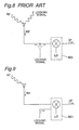
- the injection locking signal power is generally much greater than the RF signal power and this can lead to the problem of unwanted transmission of the injection locking signal from the receiver antenna. This is illustrated by the circuit block diagram shown in Fig. 8.
- Reference numeral 801 in Fig. 8 indicates the heterojunction bipolar transferred electron triode. The transmission of the locking signal from the receiver antenna is undesirable because it can interfere with other receivers.
- An object of the present invention is to provide a novel device that can solve the above problems, by improving the heterojunction bipolar transferred electron triode.
- the present invention provides a heterojunction bipolar transferred electron tetrode comprising:
- the heterojunction bipolar transferred electron tetrode of this invention has the fourth terminal which operates independently of the existing three terminals of the anode, base and cathode. This allows an injection-locking signal to be injected into a different terminal (namely, the fourth terminal or the cathode terminal) from the terminal (namely, the cathode terminal or the fourth terminal) into which the RF (or IF) signal is input, leading to good isolation between the two terminals when the heterojunction bipolar transferred electron tetrode of this invention is used as a self-oscillating mixer.
- the injection-locking signal is prevented from being transmitted from a receiver antenna when the receiver contains the heterojunction bipolar transferred electron tetrode down converter.
- the electrical signal applied to the fourth terminal or the cathode terminal (third terminal) has the effect of disturbing the electric field profile or the current density in the active layer so that a sub-harmonic locking signal applied to the fourth terminal or the cathode region can be used to stabilize the Gunn oscillation (LO) signal frequency.
- LO Gunn oscillation
- the LO signal is generated by Gunn-Hilsum oscillations in the active layer and the signal appears between the first terminal (anode terminal) and the second terminal (base terminal) (which is usually ground).
- the power of these LO oscillations is dependent on the electric field profile and the current density in the active layer, both of which are time-dependent and position-dependent.
- the LO signal power is dependent, therefore, on the cathode current since this affects the current density in the active layer.
- an RF (or IF) signal input into the cathode (third terminal) or the fourth terminal is mixed with the LO signal and the resulting IF (or RF) signal is obtained, along with the LO signal, at the output (first terminal).
- the fourth terminal can take the form of a second cathode-type structure, a second base region, or a Schottky barrier gate electrode.
- a minimum distance between the fourth terminal and the cathode region in a direction parallel to a plane of the interface between the base region and the active region may be less than twice a thickness of the active region in a direction perpendicular to the plane, in view of an angle at which an electron current flux spreads in the active region.
- the anode region, active region, and cathode region may be made of n-type semiconductors and the base region may be made of a p-type semiconductor.
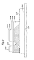
- Fig. 2 shows a simplified schematic cross-section of a first embodiment of the heterojunction bipolar transferred electron tetrode of the invention.
- the heterojunction bipolar transferred electron tetrode has a semi-insulating semiconductor substrate 201, an n-type semiconductor anode layer (anode region) 202, an n-type semiconductor active layer (active region) 203, a p-type semiconductor base layer (base region) 204, and n-type semiconductor first and second cathodes (cathode regions) 205 and 206, the layers 202-205 being sequentially stacked on the substrate 201.
- the active layer 203 covers a part of a top surface of the anode layer 202 and the base layer 204 covers an entire top surface of the active layer 203.
- the first and second cathodes 205 and 206 located on a top surface of the base layer 204 are separated from each other but in close proximity to each other.
- An anode ohmic contact metal electrode 207 is provided on the top surface of the anode layer 202 in a position spaced from the active layer 203, while a base ohmic contact metal electrode 208 is provided on the top surface of the base layer 204 in a position spaced from the cathodes 205 and 206.
- a first cathode ohmic contact metal electrode 210 and a second cathode ohmic contact metal electrode 209 are provided on the first cathode 205 and the second cathode 206, respectively, covering the greater part of their respective top surfaces.
- the fourth terminal has a second cathode-type structure located adjacent to the base layer 204 and in close proximity to the first cathode 205. If the two cathodes 205 and 206 are in close enough proximity, a sub-harmonic locking signal applied to the second cathode 206 has the effect of stabilizing the Gunn oscillation (LO) signal frequency.
- the arrows in the figure indicate the direction of flow of the electron flux. Since the electron current flux spreads out at an angle of approximately 40 degrees, as indicated in the figure, the lateral separation distance of the two cathodes 205 and 206 should be less than twice the thickness of the active layer 203.
- an input RF or IF signal is input into the first cathode 205 through the first cathode ohmic contact metal electrode 210 while the locking signal is input into the second cathode 206 through the second cathode ohmic contact metal electrode 209.
- These cathodes 205 and 206 are electrically well isolated from each other.
- the locking signal is prevented from being transmitted from an antenna of the receiver or transmitter in which the heterojunction bipolar transferred electron tetrode is included.
- the injection locking signal well achieves the function of disturbing the electric field profile and the current density in the active layer 203.
- the Gunn oscillation (LO) signal frequency is effectively stabilized.
- more than two cathodes having their own electrodes may be disposed adjacent to the base region.
- Fig. 3 shows a simplified schematic cross-section of a second embodiment of the heterojunction bipolar transferred electron tetrode of the invention.
- the heterojunction bipolar transferred electron tetrode has a semi-insulating semiconductor substrate 301, an n-type semiconductor anode layer (anode region) 302, an n-type semiconductor active layer (active region) 303, p-type semiconductor first and second base layers (base regions) 304 and 306, and an n-type semiconductor cathode (cathode region) 305, the layers 302-305 being sequentially stacked on the substrate 301.
- the active layer 303 covers a part of a top surface of the anode layer 302.
- the first and second base layers 304 and 306 located on a top surface of the active layer 303 are separated from each other but in close proximity to each other.
- the cathode 305 covers a part of a top surface of the first base layer 304.
- An anode ohmic contact metal electrode 307 is provided on the top surface of the anode layer 302 in a position spaced from the active layer 303.
- a first base ohmic contact metal electrode 308 is provided on the top surface of the first base layer 304 in a position spaced from the cathode 305.
- a cathode ohmic contact metal electrode 310 and a second base ohmic contact metal electrode 309 are provided on the cathode 305 and the second base layer 306, respectively. These electrodes 310 and 309 cover the greater part of the respective top surface of the cathode 305 and the base layer 306.
- the fourth terminal takes the form of a second base layer 306 located adjacent to the active layer 303 and in close proximity to the first base layer 304.
- a sub-harmonic locking signal applied to the second base layer 306 has the effect of stabilizing the Gunn oscillation (LO) signal frequency if the electric field generated by the signal penetrates far enough into the active layer 303 to disturb the electric field profile in the region in which Gunn oscillations are occurring.
- the arrows in Fig. 3 indicate the direction of flow of the electron flux. Since the lateral penetration distance of the electric field is approximately equal to the vertical penetration distance, the lateral separation distance between the second base region 306 and the cathode 305 should be less than twice the thickness of the active layer 303.
- the injection locking signal well achieves the function of disturbing the electric field profile and the current density in the active layer 303.
- the Gunn oscillation (LO) signal frequency is effectively stabilized.
- three or more base regions having their own electrodes may be formed adjacent to the active region.
- two or more base regions may be located between the active region and the associated cathode regions.
- Fig. 4 shows a simplified schematic cross-section of a third embodiment of the heterojunction bipolar transferred electron tetrode of the invention.
- the heterojunction bipolar transferred electron tetrode has a semi-insulating semiconductor substrate 401, an n-type semiconductor anode layer (anode region) 402, an n-type semiconductor active layer (active region) 403, a p-type semiconductor base layer (base region) 404, and an n-type semiconductor cathode (cathode region) 405, the layers 402-405 being sequentially stacked on the substrate 401.
- the active layer 403 covers a part of a top surface of the anode layer 402, the base layer 404 covers a part of a top surface of the active layer 403, and the cathode 405 covers a part of a top surface of the base layer 404.
- An anode ohmic contact metal electrode 407 is provided on the top surface of the anode layer 402 in a position spaced from the active layer 403.
- a Schottky barrier metal gate electrode 406 is provided on the top surface of the active layer 403 in a position spaced from the base layer 404.
- a base ohmic contact metal electrode 408 is provided on the top surface of the base layer 404 in a position spaced from the cathode 405, and a cathode ohmic contact metal electrode 409 is provided on a top surface of the cathode 405, covering the greater part of the top surface.
- the fourth terminal has the form of a Schottky barrier metal gate electrode 406 located adjacent to the active layer 403 and in close proximity to the base layer 404.
- a sub-harmonic locking signal applied to the Schottky barrier metal gate electrode 406 has the effect of stabilizing the Gunn oscillation (LO) signal frequency if the electric field generated by the signal penetrates far enough into the active layer 403 to disturb the electric field profile in the region in which Gunn oscillations are occurring.
- the arrows in Fig. 4 indicate the direction of flow of the electron flux.
- the operation of the third embodiment is similar to that of the second embodiment with dual base regions and the lateral separation distance between the gate electrode 406 and the cathode 405 should be less than twice the thickness of the active layer 403.
- an input (RF or IF) signal is input into the cathode 405 through the cathode ohmic contact metal electrode 409 while the locking signal is input into the Schottky barrier metal gate electrode 406.
- Good electrical isolation between the gate electrode 406 and the cathode terminal 409,405 is achieved.
- the locking signal is prevented from being transmitted from an antenna of the receiver or transmitter in which the heterojunction bipolar transferred electron tetrode is included.
- the injection locking signal applied to the gate electrode 406 well achieves the function of disturbing the electric field profile and the current density in the active layer 403.
- the Gunn oscillation (LO) signal frequency is effectively stabilized.
- the input (RF or IF) terminal would be interchanged with the locking signal terminal.
- the input (RF or IF) signal would be applied to the second cathode 206 and the locking signal applied to the first cathode 205.
- the input (RF or IF) signal would be applied to the second base terminal 306 and the locking signal applied to the cathode 305.
- the input (RF or IF) signal would be applied to the Schottky barrier metal electrode 406 and the locking signal applied to the cathode 405.
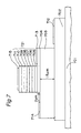
- Fig. 1 shows a schematic cross-section of one example of the above-mentioned first embodiment.
- N D and N A represent the donor impurity doping concentration and the acceptor impurity doping concentration, respectively. Also, an arrow " ⁇ " between two numerical values indicates a gradual change from one value to the other value as moving from the substrate side toward the device top surface side.
- An AuGe/Ni/Au anode ohmic contact electrode 112 is provided on the top surface of the anode layer 102 in a position spaced from the active layer 103, while a Ti/Pt/Au base ohmic contact electrode 113 is provided on the top surface of the base layer 104 in a position spaced from the cathodes 121 and 122. Also, a WN/Ti/Pt/Au first cathode ohmic contact electrode 115 and a WN/Ti/Pt/Au second cathode ohmic contact electrode 114 are provided on the first cathode 121 and the second cathode 122, respectively. These electrodes 115, 114 cover the greater part of the top surfaces of the cathodes 121, 122.
- the fourth terminal has a second cathode-type structure 122 located adjacent to the base layer 104 in close proximity to the first cathode 121.
- the active layer 103 has a thickness of 1.1 ⁇ m and the lateral separation between the two cathodes 121 and 122 is 2 ⁇ m, as indicated in Fig. 1. That is, the lateral separation distance of the two cathodes 121 and 122 is less than twice the thickness of the active layer 103.
- a sub-harmonic locking signal applied to the cathode 122 or 121 has the effect of stabilizing the Gunn oscillation (LO) signal frequency.
- LO Gunn oscillation
- Fig. 5 shows a schematic cross-section of a modification of the Fig. 1 example of the first embodiment.
- An AuGe/Ni/Au anode ohmic contact electrode 512 is provided on the top surface of the anode layer 502 in a position spaced from the active layer 503.
- a Ti/Pt/Au base ohmic contact electrode 513 is provided on the top surface of the base layer 504 in a position spaced from the cathodes 521 and 522.
- a WN/Ti/Pt/Au first cathode ohmic contact electrode 515 and a WN/Ti/Pt/Au second cathode ohmic contact electrode 514 are provided on the first laminated cathode 521 and the second laminated cathode 522, respectively.
- the InGaP passivation layer 505 is included in the device structure. Since the InGaP layer 505 is depleted of electrons, the cathodes 521 and 522 are electrically isolated from each other. As indicated in Fig. 5, the active layer 503 has a thickness of 1.8 ⁇ m and the minimum lateral separation distance between the two cathodes is 2 ⁇ m. That is, the lateral separation distance of the two cathodes 521 and 522 is less than twice the thickness of the active layer 503. Thus, a sub-harmonic locking signal applied to the cathode 522 or 521 has the effect: of stabilizing the Gunn oscillation (LO) signal frequency.
- LO Gunn oscillation
- Fig. 6 shows a schematic cross-section of an example of the device structure according to the second embodiment.
- An AuGe/Ni/Au anode ohmic contact electrode 612 is provided on the top surface of the anode layer 602 in a position spaced from the active layer 603.
- a Ti/Pt/Au first base ohmic contact electrode 613 is provided on the top surface of the first base layer 604 in a position spaced from the cathode 621.
- a WN/Ti/Pt/Au cathode ohmic contact electrode 615 and a Ti/Pt/Au second base ohmic contact electrode 614 are provided on the top surfaces of the cathode 621 and of the second base layer 616, respectively.
- the fourth terminal has the form of a second base layer 616 located adjacent to the active layer 603 in close proximity to the first base layer 604.
- the active layer 603 has a thickness of 1.1 ⁇ m and the lateral separation between the cathode 621 and the second base region 616 is 2 ⁇ m, as indicated in the figure. That is, the lateral separation distance of the cathode 621 and the second base region 616 is less than twice the thickness of the active layer 603.
- a sub-harmonic locking signal applied to the second base layer 616 or cathode 621 has the effect of stabilizing the Gunn oscillation (LO) signal frequency.
- LO Gunn oscillation
- An AuGe/Ni/Au anode ohmic contact electrode 712 is provided on the top surface of the anode layer 702 in a position spaced from the active layer 703.
- a Schottky barrier gate electrode 714 is provided on the active layer 703 in a separated manner from but in close proximity to the base layer 704.
- a Ti/Pt/Au base ohmic contact electrode 713 is provided on the top surface of the base layer 704 in a position spaced from the cathode 721.
- a WN/Ti/Pt/Au cathode ohmic contact electrode 715 is provided on the top surface of the cathode 721.
- the fourth terminal has the form of a Schottky barrier gate electrode 714 located adjacent to the active layer 703 in close proximity to the base region 704.
- the active layer 703 has a thickness of 1.5 ⁇ m and the lateral separation between the cathode 721 and the Schottky barrier gate electrode 714 is 2 ⁇ m, as indicated in Fig. 7. That is, the minimum lateral separation distance of the cathode 721 and the gate electrode 714 is less than twice the thickness of the active layer 703.
- a sub-harmonic locking signal applied to the Schottky barrier gate electrode 714 or the cathode 721 has the effect of stabilizing the Gunn oscillation (LO) signal frequency.
- LO Gunn oscillation
- the heterojunction bipolar transferred electron tetrode in any one of the above-mentioned embodiments has good electrical isolation between the injection-locking signal and the input (RF or IF) signal when used in a receiver, as shown in Fig. 9, as a self-oscillating mixer 901.
- the high degree of electrical isolation arises because of the high impedance between the input (RF or IF) terminal and the terminal into which the locking signal is applied. This isolation between the input terminal and the locking signal terminal prevents the unwanted transmission of the locking signal from the antenna in the receiver.
Landscapes
- Bipolar Transistors (AREA)
Abstract
Description
Claims (14)
- A heterojunction bipolar transferred electron tetrode comprising:an anode region (102, 202, 302, 402, 502, 602, 702) providing a first terminal as an output terminal;an active region (103, 213, 303, 403, 503, 603, 703) in which Gunn-Hilsum oscillations are generated;a base region (104, 204, 304, 404, 504, 604, 704) providing a second terminal;a cathode region (121, 205, 305, 405, 521, 621, 721) providing a third terminal;said anode region, active region, base region, and cathode region being provided sequentially, anda fourth terminal (122, 206, 306, 406, 522, 616, 714) which is operable independently of each of said three terminals, and whereinsaid cathode region and fourth terminal are in proximity enough to each other such that one of said cathode region and said fourth terminal is usable as an input terminal and that the other of said cathode region and said fourth terminal is usable as a terminal to which an electrical signal for disturbing an electric field profile or a current density in the active region is applied.
- The heterojunction bipolar transferred electron tetrode according to claim 1, wherein a minimum distance between said cathode region and said fourth terminal in a direction parallel to a plane of an interface between said base region and said active region is less than twice a thickness of said active region in a direction perpendicular to said plane.
- The heterojunction bipolar transferred electron tetrode according to claim 1 or 2, wherein said anode region (102, 202, 302, 402, 502, 602, 702), active region (103, 203, 303, 403, 503, 603, 703), and cathode region (121, 205, 305, 405, 521, 621, 721) are made of n-type semiconductors and said base region (104, 204, 304, 404, 504, 604, 704) is made of a p-type semiconductor.
- The heterojunction bipolar transferred electron tetrode according to any one of claims 1 - 3, whereinsaid fourth terminal is constituted of a second cathode region (122, 206, 522);each cathode region (121, 122; 205, 206; 521, 522) is located adjacent to said base region (104, 204, 504) and has its own independent electrode (115, 114; 210, 209; 515, 514);materials of said cathode regions, base region, active region (103, 203, 503) and anode region (102, 202, 502) are III-V semiconductor compounds containing one or more of group III elements of Ga, In or Al and one or more of group V elements of As, P or N; andsaid active region has a doping concentration that decreases with increasing distance from an interface between said active region and said base region.
- The heterojunction bipolar transferred electron tetrode according to claim 4, further comprising a mobile charge-depleted layer (505) between said base region (504) and said cathodes (521, 522).
- The heterojunction bipolar transferred electron tetrode according to any one of claims 1 - 3, whereinsaid fourth terminal is constituted of a second base region (306, 616);each base region (304, 306; 604, 616) is located adjacent to said active region (303, 603) and has its own independent electrode (308, 309; 613, 614);materials of said cathode region (305, 621), base regions, active region and anode region (302, 602) are III-V semiconductor compounds containing one or more of group III elements of Ga, In and Al and one or more of group V elements of As, P and N; andsaid active region has a doping concentration that decreases with increasing distance from an interface between said active region and said base region.
- The heterojunction bipolar transferred electron tetrode according to any one of claims 1 - 3, whereinsaid fourth terminal is constituted of a Schottky barrier gate electrode (406, 714) formed on said active layer (403, 703);materials of said cathode region (405, 721), base region (404, 704), active region and anode region (402, 702) are III-V semiconductor compounds containing one or more of group III elements of Ga, In and Al and one or more of group V elements of As, P and N; andsaid active region has a doping concentration that decreases with increasing distance from an interface between said active region and said base region.
- A heterojunction bipolar transferred electron tetrode comprising:an n-type semiconductor anode region (102, 202, 502);an n-type semiconductor active region (103, 203, 503);a p-type semiconductor base region (104, 204, 504); anda plurality of n-type semiconductor cathode regions (121, 122; 205, 206; 521, 522), and whereineach cathode region is located adjacent to the base region and has its own independent electrode (115, 114; 210, 209; 515, 514);materials of the cathode regions, base region, active region and anode region are III-V semiconductor compounds containing one or more of group III elements Ga, In and Al and one or more of group V elements As, P and N; andthe active region has a doping concentration ND that decreases with increasing distance from an interface of the base region and the active region.
- The heterojunction bipolar transferred electron tetrode according to claim 8, in which:
a minimum distance between adjacent cathode regions (121, 122; 205, 206; 521, 522) in a direction parallel to a plane of the interface between the base region and the active region is less than twice a thickness of the active region in a direction perpendicular to the plane of the interface between the base and the active region. - A heterojunction bipolar transferred electron tetrode, comprising:an n-type semiconductor anode region (302, 602);an n-type semiconductor active region (303, 603);a plurality of p-type semiconductor base regions (304, 306; 604, 616); andat least one n-type semiconductor cathode region (305, 621), and whereineach base region is located adjacent to the active region and has its own independent electrode (308, 309; 613, 614);at least one base region is located between the active region and the cathode region (304, 604);materials of the cathode regions, base region, active region and anode region are III-V semiconductor compounds containing one or more of group III elements Ga, In and Al and one or more of group V elements As, P and N; andthe active region has a doping concentration ND that decreases with increasing distance from an interface of the base region and the active region.
- The heterojunction bipolar transferred electron tetrode according to claim 10, in which:
a minimum distance between adjacent base regions (304, 306; 604, 616) in a direction parallel to a plane of the interface between the base region and the active region is less than twice a thickness of the active layer in a direction perpendicular to the plane of the interface between the base region and the active region. - A heterojunction bipolar transferred electron tetrode, comprising:an n-type semiconductor anode region (402, 702);an n-type semiconductor active region (403, 703);at least one p-type semiconductor base region (404, 704);at least one n-type semiconductor cathode region (405, 721); and whereinat least one Schottky barrier gate electrode (406, 714) is formed on the active layer;each base region (404, 704) is located adjacent to the active region (403, 703) and has its own independent electrode;at least one base region is located between the active region and the cathode region;materials of the cathode region, base region, active region, and anode region are III-V semiconductor compounds containing one or more of group III elements Ga, In and Al and one or more of group V elements As, P and N; andthe active region has a doping concentration ND that decreases with increasing distance from an interface of the base region and the active region.
- The heterojunction bipolar transferred electron tetrode according to claim 12, in which:
a minimum distance between a said Schottky barrier gate electrode (406, 714) and a said cathode region (405, 721) in a direction parallel to a plane of the interface between the base region and the active region is less than twice a thickness of the active layer in a direction perpendicular to the plane of the interface between the base and the active region. - A heterojunction bipolar transferred electron device comprising anode, active, base and cathode regions provided sequentially in the stated order, and arranged for Gunn-Hilsum oscillations to be generated in the active region, characterized by an independently operable terminal provided close enough to the cathode region so that an electrical signal applied to one of the cathode region and the terminal disturbs an electric field profile or a current density in the active region due to an input signal applied to the other of the cathode region and the terminal, thereby stabilizing the Gunn oscillation signal frequency.
Applications Claiming Priority (2)
| Application Number | Priority Date | Filing Date | Title |
|---|---|---|---|
| JP2000094304A JP4598224B2 (en) | 2000-03-30 | 2000-03-30 | Heterojunction bipolar gun effect four-terminal device |
| JP2000094304 | 2000-03-30 |
Publications (3)
| Publication Number | Publication Date |
|---|---|
| EP1139452A2 true EP1139452A2 (en) | 2001-10-04 |
| EP1139452A3 EP1139452A3 (en) | 2004-04-28 |
| EP1139452B1 EP1139452B1 (en) | 2005-08-17 |
Family
ID=18609372
Family Applications (1)
| Application Number | Title | Priority Date | Filing Date |
|---|---|---|---|
| EP01302992A Expired - Lifetime EP1139452B1 (en) | 2000-03-30 | 2001-03-29 | Heterojunction bipolar transferred electron tetrode |
Country Status (4)
| Country | Link |
|---|---|
| US (1) | US6566694B2 (en) |
| EP (1) | EP1139452B1 (en) |
| JP (1) | JP4598224B2 (en) |
| DE (1) | DE60112641T2 (en) |
Cited By (2)
| Publication number | Priority date | Publication date | Assignee | Title |
|---|---|---|---|---|
| WO2003019692A1 (en) * | 2001-07-25 | 2003-03-06 | Forschungsverbund Berlin E.V. | Gunn effect semiconductor component such as a hetero-bipolar transistor (hbt) for generating frequency-variable oscillations |
| DE102004053393A1 (en) * | 2004-11-05 | 2006-05-11 | Atmel Germany Gmbh | Method for producing a semiconductor article and semiconductor article |
Families Citing this family (4)
| Publication number | Priority date | Publication date | Assignee | Title |
|---|---|---|---|---|
| JP2006156776A (en) * | 2004-11-30 | 2006-06-15 | Toshiba Corp | Semiconductor device |
| TW201208114A (en) * | 2010-08-02 | 2012-02-16 | Foxsemicon Integrated Tech Inc | Lighting-emitting diode structure |
| US10446532B2 (en) | 2016-01-13 | 2019-10-15 | Invensas Bonding Technologies, Inc. | Systems and methods for efficient transfer of semiconductor elements |
| CN109086480B (en) * | 2018-06-22 | 2021-10-19 | 东南大学 | A method for identifying nonlinear self-excited forces of bridge sections |
Family Cites Families (16)
| Publication number | Priority date | Publication date | Assignee | Title |
|---|---|---|---|---|
| JPH0654786B2 (en) * | 1984-12-27 | 1994-07-20 | 住友電気工業株式会社 | Heterojunction semiconductor device |
| US5352911A (en) * | 1991-10-28 | 1994-10-04 | Trw Inc. | Dual base HBT |
| US5404373A (en) * | 1991-11-08 | 1995-04-04 | University Of New Mexico | Electro-optical device |
| JP3016302B2 (en) * | 1992-04-23 | 2000-03-06 | 日本電気株式会社 | Pnpn semiconductor device and its driving circuit |
| US5365477A (en) * | 1992-06-16 | 1994-11-15 | The United States Of America As Represented By The Secretary Of The Navy | Dynamic random access memory device |
| US5298438A (en) * | 1992-08-31 | 1994-03-29 | Texas Instruments Incorporated | Method of reducing extrinsic base-collector capacitance in bipolar transistors |
| US5408107A (en) * | 1993-05-20 | 1995-04-18 | The Board Of Regents Of The University Of Texas System | Semiconductor device apparatus having multiple current-voltage curves and zero-bias memory |
| US5648666A (en) * | 1994-04-13 | 1997-07-15 | Trw Inc. | Double-epitaxy heterojunction bipolar transistors for high speed performance |
| JPH0822998A (en) * | 1994-07-06 | 1996-01-23 | Mitsubishi Electric Corp | Semiconductor device and manufacturing method thereof |
| FR2756384B1 (en) * | 1996-11-28 | 1999-02-12 | Minot Christophe | BIDIRECTIONAL DEVICE FOR TRANSPOSITION BETWEEN OPTICAL SIGNALS AND ELECTRIC SIGNALS, FOR COMMUNICATION SYSTEM |
| US5798535A (en) * | 1996-12-20 | 1998-08-25 | Motorola, Inc. | Monolithic integration of complementary transistors and an LED array |
| JP3874919B2 (en) * | 1998-02-27 | 2007-01-31 | 富士通株式会社 | Compound semiconductor device |
| US6229189B1 (en) * | 1998-12-24 | 2001-05-08 | Hughes Electronics Corporation | Multi-function optoelectronic device structure |
| JP2000299386A (en) * | 1999-04-14 | 2000-10-24 | Nec Corp | Semiconductor circuit device and method of manufacturing the same |
| JP4437342B2 (en) * | 1999-07-07 | 2010-03-24 | シャープ株式会社 | Bipolar Gun Effect Triode, Voltage Controlled Frequency Variable Oscillator, Injection Locked Oscillator, Self-Oscillating Mixer, and Radio Receiver Using It |
| JP2001210722A (en) * | 2000-01-27 | 2001-08-03 | Sharp Corp | Semiconductor device, manufacturing method thereof, millimeter wave band oscillator, and millimeter wave band communication device |
-
2000
- 2000-03-30 JP JP2000094304A patent/JP4598224B2/en not_active Expired - Fee Related
-
2001
- 2001-03-29 EP EP01302992A patent/EP1139452B1/en not_active Expired - Lifetime
- 2001-03-29 DE DE60112641T patent/DE60112641T2/en not_active Expired - Lifetime
- 2001-03-30 US US09/820,767 patent/US6566694B2/en not_active Expired - Fee Related
Non-Patent Citations (5)
| Title |
|---|
| DALLE C ET AL: "Bipolar cathode transferred-electron device for millimeter-wave generation" SOLID-STATE ELECTRONICS, JAN. 2000, ELSEVIER, UK, vol. 44, no. 1, pages 79-84, XP002271911 ISSN: 0038-1101 * |
| POSSE V A ET AL: "Gunn effect and high-injection phenomenon in heterojunction bipolar transistors" ELECTRONICS LETTERS, IEE STEVENAGE, GB, vol. 30, no. 22, 27 October 1994 (1994-10-27), pages 1893-1894, XP006001260 ISSN: 0013-5194 * |
| POSSE V A ET AL: "Novel transient phenomena in heterojunction bipolar transistors" SOLID STATE ELECTRONICS, ELSEVIER SCIENCE PUBLISHERS, BARKING, GB, vol. 41, no. 4, 1 April 1997 (1997-04-01), pages 527-530, XP004056831 ISSN: 0038-1101 * |
| POSSE V A ET AL: "Transferred-electron induced current instabilities in heterojunction bipolar transistors" APPLIED PHYSICS LETTERS, 12 JUNE 1995, USA, vol. 66, no. 24, pages 3319-3321, XP002271910 ISSN: 0003-6951 * |
| TWYNAM J K ET AL: "DEMONSTRATION OF A 77-GHZ HETEROJUNCTION BIPOLAR TRANSFERRED ELECTRON DEVICE" IEEE ELECTRON DEVICE LETTERS, IEEE INC. NEW YORK, US, vol. 21, no. 1, January 2000 (2000-01), pages 2-4, XP000890456 ISSN: 0741-3106 * |
Cited By (4)
| Publication number | Priority date | Publication date | Assignee | Title |
|---|---|---|---|---|
| WO2003019692A1 (en) * | 2001-07-25 | 2003-03-06 | Forschungsverbund Berlin E.V. | Gunn effect semiconductor component such as a hetero-bipolar transistor (hbt) for generating frequency-variable oscillations |
| DE102004053393A1 (en) * | 2004-11-05 | 2006-05-11 | Atmel Germany Gmbh | Method for producing a semiconductor article and semiconductor article |
| DE102004053393B4 (en) * | 2004-11-05 | 2007-01-11 | Atmel Germany Gmbh | Method for producing a vertically integrated cascode structure and vertically integrated cascode structure |
| US7488663B2 (en) | 2004-11-05 | 2009-02-10 | Atmel Germany Gmbh | Semiconductor article and method for manufacturing with reduced base resistance |
Also Published As
| Publication number | Publication date |
|---|---|
| US20020011605A1 (en) | 2002-01-31 |
| JP4598224B2 (en) | 2010-12-15 |
| US6566694B2 (en) | 2003-05-20 |
| DE60112641T2 (en) | 2006-06-08 |
| JP2001284682A (en) | 2001-10-12 |
| EP1139452A3 (en) | 2004-04-28 |
| DE60112641D1 (en) | 2005-09-22 |
| EP1139452B1 (en) | 2005-08-17 |
Similar Documents
| Publication | Publication Date | Title |
|---|---|---|
| US20230420526A1 (en) | Wide bandgap transistors with gate-source field plates | |
| Urteaga et al. | InP HBT technologies for THz integrated circuits | |
| US7573078B2 (en) | Wide bandgap transistors with multiple field plates | |
| EP1751803B1 (en) | Wide bandgap hemts with source connected field plates | |
| JP3677350B2 (en) | Semiconductor device and manufacturing method of semiconductor device | |
| EP1901342A1 (en) | Field effect transistor | |
| US20080203446A1 (en) | Composite contact for semiconductor device | |
| US20230208359A1 (en) | Device emitting or detecting terahertz waves, and manufacturing method for device | |
| US6794734B2 (en) | Heterojunction P-I-N diode and method of making the same | |
| US6242766B1 (en) | High electron mobility transistor | |
| Suemitsu | InP and GaN high electron mobility transistors for millimeter-wave applications | |
| EP1139452B1 (en) | Heterojunction bipolar transferred electron tetrode | |
| US6835969B1 (en) | Split-channel high electron mobility transistor (HEMT) device | |
| Irvin et al. | Fabrication and noise performance of high-power GaAs IMPATTS | |
| US20010048120A1 (en) | Heterojunction bipolar transistor composed of emitter layer which includes orderly structured layer and disorderly structured layer | |
| Vukusic et al. | HBV tripler with 21% efficiency at 102 GHz | |
| US8076700B2 (en) | P-N junction for use as an RF mixer from GHZ to THZ frequencies | |
| Hur et al. | Development of double recessed AlInAs/GaInAs/InP HEMTs for millimeter wave power applications | |
| JP4437342B2 (en) | Bipolar Gun Effect Triode, Voltage Controlled Frequency Variable Oscillator, Injection Locked Oscillator, Self-Oscillating Mixer, and Radio Receiver Using It | |
| US5665999A (en) | Metal-semiconductor diode and process for preparing metal-semiconductor diodes | |
| Krishnamurthi et al. | Millimetre-wave frequency tripling using stacked heterostructure-barrier varactors on InP | |
| JP4789489B2 (en) | Microwave monolithic integrated circuit | |
| Whelan et al. | A comparison of channel indium content in low noise metamorphic HEMTs with In/sub x/Ga/sub 1-x/As (0.3< X⩽ 0.6) | |
| Arscott et al. | Transferred-substrate InP-based heterostructure barrier varactor diodes on quartz | |
| Ohkubo et al. | High-reliability InGaP/GaAs HBTs with 153 GHz f T and 170 GHz f max |
Legal Events
| Date | Code | Title | Description |
|---|---|---|---|
| PUAI | Public reference made under article 153(3) epc to a published international application that has entered the european phase |
Free format text: ORIGINAL CODE: 0009012 |
|
| AK | Designated contracting states |
Kind code of ref document: A2 Designated state(s): AT BE CH CY DE DK ES FI FR GB GR IE IT LI LU MC NL PT SE TR |
|
| AX | Request for extension of the european patent |
Free format text: AL;LT;LV;MK;RO;SI |
|
| PUAL | Search report despatched |
Free format text: ORIGINAL CODE: 0009013 |
|
| AK | Designated contracting states |
Kind code of ref document: A3 Designated state(s): AT BE CH CY DE DK ES FI FR GB GR IE IT LI LU MC NL PT SE TR |
|
| AX | Request for extension of the european patent |
Extension state: AL LT LV MK RO SI |
|
| 17P | Request for examination filed |
Effective date: 20040623 |
|
| 17Q | First examination report despatched |
Effective date: 20040726 |
|
| AKX | Designation fees paid |
Designated state(s): DE FR GB IT |
|
| GRAP | Despatch of communication of intention to grant a patent |
Free format text: ORIGINAL CODE: EPIDOSNIGR1 |
|
| GRAS | Grant fee paid |
Free format text: ORIGINAL CODE: EPIDOSNIGR3 |
|
| GRAA | (expected) grant |
Free format text: ORIGINAL CODE: 0009210 |
|
| AK | Designated contracting states |
Kind code of ref document: B1 Designated state(s): DE FR GB IT |
|
| REG | Reference to a national code |
Ref country code: GB Ref legal event code: FG4D |
|
| REF | Corresponds to: |
Ref document number: 60112641 Country of ref document: DE Date of ref document: 20050922 Kind code of ref document: P |
|
| ET | Fr: translation filed | ||
| PLBE | No opposition filed within time limit |
Free format text: ORIGINAL CODE: 0009261 |
|
| STAA | Information on the status of an ep patent application or granted ep patent |
Free format text: STATUS: NO OPPOSITION FILED WITHIN TIME LIMIT |
|
| 26N | No opposition filed |
Effective date: 20060518 |
|
| PGFP | Annual fee paid to national office [announced via postgrant information from national office to epo] |
Ref country code: IT Payment date: 20140307 Year of fee payment: 14 Ref country code: FR Payment date: 20140311 Year of fee payment: 14 |
|
| PGFP | Annual fee paid to national office [announced via postgrant information from national office to epo] |
Ref country code: GB Payment date: 20140326 Year of fee payment: 14 |
|
| PGFP | Annual fee paid to national office [announced via postgrant information from national office to epo] |
Ref country code: DE Payment date: 20140417 Year of fee payment: 14 |
|
| REG | Reference to a national code |
Ref country code: DE Ref legal event code: R119 Ref document number: 60112641 Country of ref document: DE |
|
| GBPC | Gb: european patent ceased through non-payment of renewal fee |
Effective date: 20150329 |
|
| PG25 | Lapsed in a contracting state [announced via postgrant information from national office to epo] |
Ref country code: IT Free format text: LAPSE BECAUSE OF NON-PAYMENT OF DUE FEES Effective date: 20150329 |
|
| REG | Reference to a national code |
Ref country code: FR Ref legal event code: ST Effective date: 20151130 |
|
| PG25 | Lapsed in a contracting state [announced via postgrant information from national office to epo] |
Ref country code: GB Free format text: LAPSE BECAUSE OF NON-PAYMENT OF DUE FEES Effective date: 20150329 Ref country code: DE Free format text: LAPSE BECAUSE OF NON-PAYMENT OF DUE FEES Effective date: 20151001 |
|
| PG25 | Lapsed in a contracting state [announced via postgrant information from national office to epo] |
Ref country code: FR Free format text: LAPSE BECAUSE OF NON-PAYMENT OF DUE FEES Effective date: 20150331 |