EP1139134A2 - Coupling between optical fibre and optical element - Google Patents
Coupling between optical fibre and optical element Download PDFInfo
- Publication number
- EP1139134A2 EP1139134A2 EP01303107A EP01303107A EP1139134A2 EP 1139134 A2 EP1139134 A2 EP 1139134A2 EP 01303107 A EP01303107 A EP 01303107A EP 01303107 A EP01303107 A EP 01303107A EP 1139134 A2 EP1139134 A2 EP 1139134A2
- Authority
- EP
- European Patent Office
- Prior art keywords
- optical
- optical fiber
- face
- mount
- array
- Prior art date
- Legal status (The legal status is an assumption and is not a legal conclusion. Google has not performed a legal analysis and makes no representation as to the accuracy of the status listed.)
- Withdrawn
Links
- 230000003287 optical effect Effects 0.000 title claims abstract description 77
- 239000013307 optical fiber Substances 0.000 title claims abstract description 77
- 230000008878 coupling Effects 0.000 title description 4
- 238000010168 coupling process Methods 0.000 title description 4
- 238000005859 coupling reaction Methods 0.000 title description 4
- 239000000463 material Substances 0.000 claims abstract description 36
- 238000007689 inspection Methods 0.000 abstract 1
- 239000000758 substrate Substances 0.000 description 9
- 238000005476 soldering Methods 0.000 description 8
- 239000000835 fiber Substances 0.000 description 6
- 125000006850 spacer group Chemical group 0.000 description 5
- 238000012545 processing Methods 0.000 description 3
- 230000008054 signal transmission Effects 0.000 description 3
- 238000003466 welding Methods 0.000 description 3
- 238000003491 array Methods 0.000 description 2
- 230000005540 biological transmission Effects 0.000 description 2
- 239000000919 ceramic Substances 0.000 description 2
- WABPQHHGFIMREM-UHFFFAOYSA-N lead(0) Chemical compound [Pb] WABPQHHGFIMREM-UHFFFAOYSA-N 0.000 description 2
- 238000001465 metallisation Methods 0.000 description 2
- 238000000034 method Methods 0.000 description 2
- 238000012986 modification Methods 0.000 description 2
- 230000004048 modification Effects 0.000 description 2
- 238000012935 Averaging Methods 0.000 description 1
- 230000008859 change Effects 0.000 description 1
- 230000008602 contraction Effects 0.000 description 1
- 238000013461 design Methods 0.000 description 1
- 230000006872 improvement Effects 0.000 description 1
- 238000004519 manufacturing process Methods 0.000 description 1
- 239000004065 semiconductor Substances 0.000 description 1
Images


Classifications
-
- G—PHYSICS
- G02—OPTICS
- G02B—OPTICAL ELEMENTS, SYSTEMS OR APPARATUS
- G02B6/00—Light guides; Structural details of arrangements comprising light guides and other optical elements, e.g. couplings
- G02B6/24—Coupling light guides
- G02B6/42—Coupling light guides with opto-electronic elements
- G02B6/4201—Packages, e.g. shape, construction, internal or external details
- G02B6/4204—Packages, e.g. shape, construction, internal or external details the coupling comprising intermediate optical elements, e.g. lenses, holograms
- G02B6/4207—Packages, e.g. shape, construction, internal or external details the coupling comprising intermediate optical elements, e.g. lenses, holograms with optical elements reducing the sensitivity to optical feedback
-
- G—PHYSICS
- G02—OPTICS
- G02B—OPTICAL ELEMENTS, SYSTEMS OR APPARATUS
- G02B6/00—Light guides; Structural details of arrangements comprising light guides and other optical elements, e.g. couplings
- G02B6/24—Coupling light guides
- G02B6/42—Coupling light guides with opto-electronic elements
- G02B6/4201—Packages, e.g. shape, construction, internal or external details
- G02B6/4249—Packages, e.g. shape, construction, internal or external details comprising arrays of active devices and fibres
- G02B6/425—Optical features
-
- G—PHYSICS
- G02—OPTICS
- G02B—OPTICAL ELEMENTS, SYSTEMS OR APPARATUS
- G02B6/00—Light guides; Structural details of arrangements comprising light guides and other optical elements, e.g. couplings
- G02B6/24—Coupling light guides
- G02B6/42—Coupling light guides with opto-electronic elements
- G02B6/4201—Packages, e.g. shape, construction, internal or external details
- G02B6/4219—Mechanical fixtures for holding or positioning the elements relative to each other in the couplings; Alignment methods for the elements, e.g. measuring or observing methods especially used therefor
- G02B6/4236—Fixing or mounting methods of the aligned elements
- G02B6/4237—Welding
Definitions
- the present invention relates to an optical head comprising a mount material for fixing an optical element and a mount material for fixing an optical fiber array to which an optical fiber is connected, wherein the optical fiber is optically connected to the optical element.
- An conventional optical head comprises a mount material for fixing an optical element such as light receiving element or light emitting element and a mount material for fixing an optical fiber array to which an optical fiber is connected, wherein the optical fiber is optically connected to the optical element.
- FIG. 3 shows an optical head having a conventional light emitting element.
- An LD array 10 is provided such that a plurality of laser diodes are transversely arranged.
- a mount material 30 is made of a ALN ceramics with high heat conductivity, metalization for soldering is applied to its surface, and a wiring pattern 31 and a drive IC 35 bonded by an electrode of the LD array 10 and a wire 32 are arranged.
- the LD array 10 is fixed to the mount material 30 by means of soldering so that light emissions ejected from the LD array 10 are generally coincident with each other.
- an optical fiber array 20 has grocves 23 on a support substrate 22 in order to position optical fibers 21, and a plurality of optical fibers 21 are arranged to be housed in the V groove 23. These optical fibers are covered with a cap substrate 24 from the top, and are fixed by sheet shaped soldering, thereby forming an integral block 25.
- a support substrate 22 is protruded on the top face of a mount body 40; a spacer portion 34 is extruded on the side face of the mount material 40, and the spacer portion 34 is bonded with the side face of the mount body 40.
- this optical head is sealed with air tightness in a package by leading out an optical fiber or lead wire, whereby a parallel light transmission module is provided.
- an end face of the optical fiber 21 with which the LD array 10 is optically coupled is positioned at an end face of a block 25, and is formed so as to be opposed to a light emission plane of the mount material 30 having the LD array 10 mounted thereon.
- an interval between a light emission element required for fine adjustment and the end face of the optical fiber is spaced, adjusted, and fixed when a connection face between mounted materials fixed to each other is defined as a reference.
- This derives from light intensity in a direction orthogonal to an optical axis of an optical element for example, a laser diode and light intensity averaging between a plurality of fibers of the optical head after light axis alignment.
- the light intensity in a direction orthogonal to an optical axis of a laser diode draws a Gaussian curve shape when an optical axis is defined as a center axis.
- a point orthogonal to the optical axis is spaced from a laser diode, a top of the curve is lowered, and the gradient is gentle.
- the top of the curve is low, light intensity is lowered.
- the gradient is gentle, even if slight deviation from the optical axis occurs in a vertical direction, it indicates that a small rapid change occurs with light intensity.
- optical head even if the same optical intensity is input to a plurality of configured fibers, large deviation in light intensity must not be present between fibers due to deviation from the light axis.
- the arrangement precision of a plurality of optical elements and the arrangement precision of a plurality of fibers must be permitted to some extent in view of manufacture. This means that another optical element and an optical fiber deviation from an optical axis even if an arbitrary optical element and the corresponding optical fiber are completely aligned with the axis. Even under such circumference, as means for preventing large deviation in light intensity between fibers, there has been conventionally performed means for spacing an optical element and an optical fiber from each other by a predetermined value. This method utilizes the fact that, although light intensity is lowered as deviation from an optical element is more significant as described above, the variation rate of light intensity in a direction vertical to an optical axis is gentle.
- a light emission element is fixed to a mount material by means of soldering; an optical fiber is pressed by from the top arranged and housed in a support substrate having a V groove punched thereon, and is fixed by means of soldering; and the support substrate is fixed to a top face of the mount material.
- the fixing position of the light emission element is adjusted by the mount material via a spacer for ensuring a design space.
- the position of a support substrate is fine adjusted while sensing the light receiving capability of an optical fiber fixed to the support substrate against the adjustment light from the light emission element.
- an optical head comprising a mount material for fixing an optical element and a mount material for fixing an optical fiber array, the optical fiber being optically connected to the optical element, wherein an angle formed between a light emission receiving face of the optical element and an end face of the optical fiber is 1 to 8 degrees. In this manner, an angle formed between a light emission receiving face and an end face of an optical fiber is greater than 1 degree.
- noise produced by reflection light deriving from a light receiving face or an end face of an optical fiber opposed to a light emitting element is reduced as compared with a case in which the conventional light emission receiving face and the end face of the optical fiber are substantially parallel to each other, and a failure with optical signal transmission can be prevented.
- an angle formed between the light emission receiving face and an end face of the optical fiber is smaller than 8 degrees, and thus, bonding efficiency is improved.
- an end face can be shaved with high processing precision, and thus, the shaved portion can act as the above spacing distance . Therefore, the spacing distance can be ensured with high precision.
- an optical head wherein thermal expansion rates of the mount material of the optical element and the mount material of the optical fiber array are substantially equal to a thermal expansion rate of the optical fiber array material.
- the thermal expansion rates of mount materials is substantially identical to each other.
- an optical head wherein the optical fiber is a single mode, and the mount material of the optical element and the mount material of the optical fiber array are spot welded, such as Yag melded each other.
- the mount material of the optical element and the mount material of the optical fiber array are spot welded, such as Yag melded each other.
- FIG. 1 is an illustrative view illustrating an optical head having a light emitting element according to the present invention.
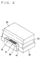
- FIG. 2 is a perspective view showing the optical head.
- This optical head comprises: an LD array 10 driven by an IC, the LD array emitting light; an optical fiber array 20 arranging and fixing optical fibers 21 in one or more arrays; a mount material 30 for fixing the LD array 10; and a mount material 40 for fixing the optical fiber array 20, wherein the optical head is optically coupled with an optical fiber 21 in the LD array 10.
- the LD array 10 has a plurality of semiconductor lasers transversely arranged thereon.
- the mount material 30 is made of a SiC ceramics with high thermal conductivity, metalization for soldering is applied onto its surface, and a wiring pattern 31 bonded by an electrode of the LD array 10 and a wire 32 is arranged.
- the light ejected from the LD array 10 is fixed to the mount material 30 by means of soldering with the LD arrays 10 being aligned on their end faces so as to be generally horizontal in a horizontal direction.
- V grooves 23 are formed on a support substrate 22 in order to position optical fibers 21; a plurality of optical fibers 21 are housed and arranged in V grooves 23, and a cap substrate 24 is covered over the fibers and fixed by sheet shaped soldering, thereby forming an integral block 25. Then, at a position at which the optical fiber 20 and the LD array 10 are optical coupled with each other, and a mount material 30 of the LD array 10 is bonded with the side face of the mount body 40 at a spot welding portion 41 caused by Yag lasers. This bonding is done by spot welding, and thus, there is no substantial welding strain, and desired optical coupling does not break.
- this optical head is sealed with air tightness in a package by leading out an optical fiber or lead wire, whereby a parallel light transmission module is provided.
- each optical fiber 21 with which the LD array 10 is optical coupled is positioned on an inclined face of a block 25, and an inclined angle ⁇ is defined as 2 degrees relative to the light emitting plane of the mount material having the opposite LD array 10 mounted thereon.
- This inclined angle ⁇ is properly 1 to 8 degrees.
- a gap can be formed by shaving the end face with high processing precision.
- the angle ⁇ formed between the light emission receiving face and the end face of the optical fiber is smaller than 8 degrees, and thus, coupling efficiency is improved.
- the shown inclined angle ⁇ is indicated in an exaggerated manner, and two-dot and chain line indicates the external line of a conventional box-shaped block.
- an optical head according to the present invention is capable of reducing noise produced by reflection light deriving from an end face of an optical fiber opposed to a light receiving face or light emitting element as compared with a conventional optical head in which a light emission receiving face and an end face of an optical fiber are substantially parallel to each other; preventing an optical signal transmission failure; and shaving an end face with high processing precision.
- an angle formed between the light emission face and the end face of the optical fiber is smaller than 8 degrees, and thus, an optical head with high coupling efficiency can be provided without using a spacer.
Landscapes
- Physics & Mathematics (AREA)
- General Physics & Mathematics (AREA)
- Optics & Photonics (AREA)
- Optical Couplings Of Light Guides (AREA)
- Optical Communication System (AREA)
- Led Device Packages (AREA)
- Led Devices (AREA)
- Light Receiving Elements (AREA)
Abstract
Description
Claims (8)
- An optical head comprising a mount for fixing an optical element and a mount for fixing an optical fiber array, the optical fiber being optically connected to the optical element, wherein the angle formed between a light emission or receiving face of the optical element and an end face of the optical fiber is in the range 1 to 8 degrees.
- An optical head as claimed in claim 1 wherein thermal expansion rates of the mount of the optical element and the mount of the optical fiber array are substantially equal to a thermal expansion rate of the optical fiber material.
- An optical head as claimed in claim 1 or 2 wherein the optical fiber is a single mode, and the mount of the optical element and the mount of the optical fiber array are spot welded to each other.
- An optical head comprising a mount for fixing an optical element and a mount for fixing an optical fiber, the optical fiber being optically connected to the optical element, wherein the angle formed between a light emission or receiving face of the optical element and an end face of the optical fiber is in the range 1 to 8 degrees.
- An optical head as claimed in claim 1 wherein thermal expansion rates of the mount of the optical element and the mount of the optical fiber are substantially equal to a thermal expansion rate of the optical fiber material.
- An optical head as claimed in claim 1 or 2 wherein the optical fiber is a single mode, and the mount of the optical element and the mount of the optical fiber are spot welded to each other.
- An optical head having an optical fiber aligned on an axis with an optical element, the optical fiber having its face opposed to said optical element at an angle in the range 1° to 8° to a plane perpendicular to said axis.
- An optical head as claimed in any one of claims 4 to 7, wherein the optical fiber is present in an optical fiber array.
Applications Claiming Priority (2)
| Application Number | Priority Date | Filing Date | Title |
|---|---|---|---|
| JP2000099916A JP2001281506A (en) | 2000-03-31 | 2000-03-31 | Light head |
| JP2000099916 | 2000-03-31 |
Publications (2)
| Publication Number | Publication Date |
|---|---|
| EP1139134A2 true EP1139134A2 (en) | 2001-10-04 |
| EP1139134A3 EP1139134A3 (en) | 2003-01-15 |
Family
ID=18614199
Family Applications (1)
| Application Number | Title | Priority Date | Filing Date |
|---|---|---|---|
| EP01303107A Withdrawn EP1139134A3 (en) | 2000-03-31 | 2001-04-02 | Coupling between optical fibre and optical element |
Country Status (3)
| Country | Link |
|---|---|
| US (2) | US6644867B2 (en) |
| EP (1) | EP1139134A3 (en) |
| JP (1) | JP2001281506A (en) |
Families Citing this family (4)
| Publication number | Priority date | Publication date | Assignee | Title |
|---|---|---|---|---|
| KR100811883B1 (en) | 2005-12-08 | 2008-03-10 | 한국전자통신연구원 | Optical arrangement method and device |
| JP4929821B2 (en) * | 2006-04-27 | 2012-05-09 | オムロン株式会社 | Optical transmission module |
| US20120288231A1 (en) * | 2011-05-11 | 2012-11-15 | Applied Optoelectronics, Inc. | Laser package including tilted laser and method of using same |
| CN103415799B (en) | 2011-05-18 | 2016-06-08 | 松下知识产权经营株式会社 | Semiconductor laser module and manufacture method thereof |
Family Cites Families (14)
| Publication number | Priority date | Publication date | Assignee | Title |
|---|---|---|---|---|
| JPS57138191A (en) * | 1981-02-19 | 1982-08-26 | Kokusai Denshin Denwa Co Ltd <Kdd> | United structure of semiconductor laser and optical fiber |
| JPS6043889A (en) * | 1983-08-22 | 1985-03-08 | Hitachi Ltd | Light-emitting device |
| US4803361A (en) * | 1986-05-26 | 1989-02-07 | Hitachi, Ltd. | Photoelectric device with optical fiber and laser emitting chip |
| US4995025A (en) * | 1986-10-06 | 1991-02-19 | Schulze Dieter M | Spherical pivoting actuator for read/record head |
| FR2605418B1 (en) * | 1986-10-17 | 1990-04-20 | Thomson Semiconducteurs | MODULE FOR COUPLING BETWEEN A SEMICONDUCTOR DEVICE AND AN OPTICAL FIBER, AND METHOD FOR ALIGNING THE SEMICONDUCTOR DEVICE AND THE FIBER |
| JP3160407B2 (en) | 1993-02-12 | 2001-04-25 | 日本碍子株式会社 | Optical fiber connection method |
| CA2135777C (en) | 1993-04-02 | 2003-03-18 | Takashi Shigematsu | Optical fiber end portion, method for manufacturing the same, and construction for connecting end portion to optical device |
| US5535296A (en) | 1994-09-28 | 1996-07-09 | Optobahn Corporation | Integrated optoelectronic coupling and connector |
| JP3472660B2 (en) * | 1995-06-22 | 2003-12-02 | 日本オプネクスト株式会社 | Optical semiconductor array module, assembling method thereof, and external substrate mounting structure |
| JPH0990174A (en) * | 1995-09-28 | 1997-04-04 | Furukawa Electric Co Ltd:The | Semiconductor laser module |
| EP0773591A3 (en) * | 1995-11-13 | 1998-09-16 | Sumitomo Electric Industries, Ltd. | Light emitting/detecting module |
| US6850475B1 (en) * | 1996-07-30 | 2005-02-01 | Seagate Technology, Llc | Single frequency laser source for optical data storage system |
| US6332719B1 (en) * | 1997-06-25 | 2001-12-25 | Matsushita Electric Industrial Co., Ltd. | Optical transmitter/receiver apparatus, method for fabricating the same and optical semiconductor module |
| US6332721B1 (en) * | 1998-07-10 | 2001-12-25 | Mitsubishi Chemical Corp. | Laser diode module |
-
2000
- 2000-03-31 JP JP2000099916A patent/JP2001281506A/en active Pending
-
2001
- 2001-03-20 US US09/812,721 patent/US6644867B2/en not_active Expired - Fee Related
- 2001-04-02 EP EP01303107A patent/EP1139134A3/en not_active Withdrawn
-
2003
- 2003-05-15 US US10/439,253 patent/US6804425B2/en not_active Expired - Fee Related
Also Published As
| Publication number | Publication date |
|---|---|
| US6644867B2 (en) | 2003-11-11 |
| US20010041031A1 (en) | 2001-11-15 |
| JP2001281506A (en) | 2001-10-10 |
| US6804425B2 (en) | 2004-10-12 |
| EP1139134A3 (en) | 2003-01-15 |
| US20030198443A1 (en) | 2003-10-23 |
Similar Documents
| Publication | Publication Date | Title |
|---|---|---|
| US5901262A (en) | Optical coupling module and method for producing the same | |
| US8213479B2 (en) | High power diode laser having multiple emitters and method for its production | |
| US6010251A (en) | Laser diode modules converging parts, and optical coupling methods | |
| US6511235B2 (en) | Integrated surface-emitting optoelectronic module and the method for making the same | |
| EP0948104B1 (en) | Semiconductor laser module and method of manufacturing the same | |
| US6366396B1 (en) | Semiconductor laser module and an optical amplifier installing the same | |
| US20020094175A1 (en) | Alignment of optical assemblies | |
| US6381386B1 (en) | V-shaped optical coupling structure | |
| US6644867B2 (en) | Optical head | |
| US4944569A (en) | Multi-fiber alignment package for optoelectronic components | |
| JP2002537636A (en) | Diode pump type multiple beam imaging system | |
| US6813102B2 (en) | Optical module with a monitor photo diode | |
| US5544184A (en) | Semiconductor illumination system with expansion matched components | |
| US20020044323A1 (en) | Module for optical communication | |
| JPH02154208A (en) | Parallel transmission optical module | |
| JPH0339706A (en) | Optical module | |
| JP2001007432A (en) | Semiconductor light emitting device | |
| US6867796B1 (en) | Semiconductor laser array and optical scanner | |
| JPH05203841A (en) | Optical coupling structure of semiconductor laser array and single mode fiber array | |
| US7162126B2 (en) | Optical module having a semiconductor optical device mounted on a bared cladding of an optical fiber | |
| EP1160600A1 (en) | Semiconductor laser diode module | |
| JP2002107582A (en) | Optical module | |
| JPH06120564A (en) | Semiconductor device with optical fiber and manufacturing method thereof | |
| KR20020039935A (en) | Optical integrated circuit device having protrusion, fabrication method of the same and module of optical communication transmission and receiving apparatus using the same | |
| KR0141188B1 (en) | Laser diode package |
Legal Events
| Date | Code | Title | Description |
|---|---|---|---|
| PUAI | Public reference made under article 153(3) epc to a published international application that has entered the european phase |
Free format text: ORIGINAL CODE: 0009012 |
|
| AK | Designated contracting states |
Kind code of ref document: A2 Designated state(s): AT BE CH CY DE DK ES FI FR GB GR IE IT LI LU MC NL PT SE TR |
|
| AX | Request for extension of the european patent |
Free format text: AL;LT;LV;MK;RO;SI |
|
| PUAL | Search report despatched |
Free format text: ORIGINAL CODE: 0009013 |
|
| AK | Designated contracting states |
Kind code of ref document: A3 Designated state(s): AT BE CH CY DE DK ES FI FR GB GR IE IT LI LU MC NL PT SE TR |
|
| AX | Request for extension of the european patent |
Free format text: AL;LT;LV;MK;RO;SI |
|
| AKX | Designation fees paid |
Designated state(s): DE FR GB |
|
| STAA | Information on the status of an ep patent application or granted ep patent |
Free format text: STATUS: THE APPLICATION IS DEEMED TO BE WITHDRAWN |
|
| 18D | Application deemed to be withdrawn |
Effective date: 20030716 |