EP1139122A2 - Optoelectric integrated device having a three-dimensional solid configuration - Google Patents
Optoelectric integrated device having a three-dimensional solid configuration Download PDFInfo
- Publication number
- EP1139122A2 EP1139122A2 EP01107915A EP01107915A EP1139122A2 EP 1139122 A2 EP1139122 A2 EP 1139122A2 EP 01107915 A EP01107915 A EP 01107915A EP 01107915 A EP01107915 A EP 01107915A EP 1139122 A2 EP1139122 A2 EP 1139122A2
- Authority
- EP
- European Patent Office
- Prior art keywords
- light
- semiconductor crystal
- ball
- emitting
- receiving
- Prior art date
- Legal status (The legal status is an assumption and is not a legal conclusion. Google has not performed a legal analysis and makes no representation as to the accuracy of the status listed.)
- Withdrawn
Links
Images


Classifications
-
- G—PHYSICS
- G02—OPTICS
- G02B—OPTICAL ELEMENTS, SYSTEMS OR APPARATUS
- G02B6/00—Light guides; Structural details of arrangements comprising light guides and other optical elements, e.g. couplings
- G02B6/10—Light guides; Structural details of arrangements comprising light guides and other optical elements, e.g. couplings of the optical waveguide type
- G02B6/12—Light guides; Structural details of arrangements comprising light guides and other optical elements, e.g. couplings of the optical waveguide type of the integrated circuit kind
- G02B6/12004—Combinations of two or more optical elements
-
- G—PHYSICS
- G02—OPTICS
- G02B—OPTICAL ELEMENTS, SYSTEMS OR APPARATUS
- G02B6/00—Light guides; Structural details of arrangements comprising light guides and other optical elements, e.g. couplings
- G02B6/10—Light guides; Structural details of arrangements comprising light guides and other optical elements, e.g. couplings of the optical waveguide type
- G02B6/12—Light guides; Structural details of arrangements comprising light guides and other optical elements, e.g. couplings of the optical waveguide type of the integrated circuit kind
- G02B6/12002—Three-dimensional structures
-
- G—PHYSICS
- G02—OPTICS
- G02B—OPTICAL ELEMENTS, SYSTEMS OR APPARATUS
- G02B6/00—Light guides; Structural details of arrangements comprising light guides and other optical elements, e.g. couplings
- G02B6/10—Light guides; Structural details of arrangements comprising light guides and other optical elements, e.g. couplings of the optical waveguide type
- G02B6/12—Light guides; Structural details of arrangements comprising light guides and other optical elements, e.g. couplings of the optical waveguide type of the integrated circuit kind
- G02B6/13—Integrated optical circuits characterised by the manufacturing method
- G02B6/132—Integrated optical circuits characterised by the manufacturing method by deposition of thin films
-
- G—PHYSICS
- G02—OPTICS
- G02B—OPTICAL ELEMENTS, SYSTEMS OR APPARATUS
- G02B6/00—Light guides; Structural details of arrangements comprising light guides and other optical elements, e.g. couplings
- G02B6/10—Light guides; Structural details of arrangements comprising light guides and other optical elements, e.g. couplings of the optical waveguide type
- G02B6/12—Light guides; Structural details of arrangements comprising light guides and other optical elements, e.g. couplings of the optical waveguide type of the integrated circuit kind
- G02B2006/12035—Materials
- G02B2006/12061—Silicon
-
- G—PHYSICS
- G02—OPTICS
- G02B—OPTICAL ELEMENTS, SYSTEMS OR APPARATUS
- G02B6/00—Light guides; Structural details of arrangements comprising light guides and other optical elements, e.g. couplings
- G02B6/10—Light guides; Structural details of arrangements comprising light guides and other optical elements, e.g. couplings of the optical waveguide type
- G02B6/12—Light guides; Structural details of arrangements comprising light guides and other optical elements, e.g. couplings of the optical waveguide type of the integrated circuit kind
- G02B2006/12083—Constructional arrangements
- G02B2006/12121—Laser
-
- G—PHYSICS
- G02—OPTICS
- G02B—OPTICAL ELEMENTS, SYSTEMS OR APPARATUS
- G02B6/00—Light guides; Structural details of arrangements comprising light guides and other optical elements, e.g. couplings
- G02B6/10—Light guides; Structural details of arrangements comprising light guides and other optical elements, e.g. couplings of the optical waveguide type
- G02B6/12—Light guides; Structural details of arrangements comprising light guides and other optical elements, e.g. couplings of the optical waveguide type of the integrated circuit kind
- G02B2006/12083—Constructional arrangements
- G02B2006/12123—Diode
Definitions
- This method aims to solve the pin-bottle-neck problem by replacing a portion of the electric wiring by optical wiring.
- the total number of electric wires can be reduced owing to characteristics of non-electromagnetic induction and broad band of the optical wiring.
- the optical wiring is arranged using conventional optical fiber and semiconductor waveguides, the width of the optical path becomes far thicker than that of electric wires. Accordingly, only a limited portion of the electric wiring can be replaced by optical wiring, and the resultant configuration inevitably lacks flexibility.
- the above requirements are typically satisfied by a structure in which the light-emitting device is composed of III - V N semiconductor material, and the light-receiving device is composed of III-V N semiconductor material or SiGe.
- x is approximately equal to 0.03
- an active layer composed thereof can emit light at a wavelength of about 1.3 ⁇ m which cannot be absorbed by Si.
- LED light emitting diodes
- VCSEL vertical cavity surface emitting laser
- Crystal growth of the optical device will be described.
- Such technology as that disclosed in Japanese Patent Application Laid-Open No. 12(2000)-332229 can be used for the crystal growth of the optical device.
- a mask for selective growth is formed on a Si wafer with a (100) face, on which the electronic device is formed.
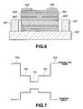
- N-type GaAs/AlAs reflective layer 602 with a reflectivity of 90 %, GaInNAs/GaAs single quantum well (SQW) active layer 603, and p-type GaAs/AlAs reflective layer 604 with a reflectivity of 90 % are formed on the wafer of the buffer layer 502.
- reflective layers 602 and 604 are provided to enhance its emission efficiency (i.e., to effectively take out much light in a desired direction).
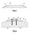
- the Si ball 101 is entirely covered with a nitride layer or the like, and a flat portion for forming an optical device thereon with a size of about 10 ⁇ m is formed by abrasion and chemical polishing.
- the (001) face and its equivalent faces (in total, six faces) are used (see Fig. 8).
- the (111) face and its equivalent faces can also be used.
- the combination of AlNAs/GaNAs is used in the n-type reflective layer 602 to achieve the lattice matching between the reflective layer 602 and the GaNAs buffer layer 502, and reduce the hetero-barrier in a conduction band of the reflective layer 604.
- a highly-reflective layer can be formed with a small number of layers, and at the same time a series resistance due to the hetero-barrier can be reduced.
- VCSEL 801 capable of operating at small current and low voltage can be achieved.
- the active layer 603 is formed of III - V N and III - V semiconductor materials to obtain the radiation wavelength (e.g., 1.3 ⁇ m) longer than a wavelength of Si absorption edge such that the interior of the Si ball 101 can be used as an optical transmission line and achieve a large band-offset in the conduction band such that thermal characteristics of the VCSEL can be improved.
- the radiation wavelength e.g., 1.3 ⁇ m
- the light-receiving device can also be fabricated by a method similar to the above fabrication method of the light source. Those optical devices can be fabricated at a time by the above selective growth technique (see Fig. 9), but the devices can be separately fabricated by the selective growth. Fig. 8 illustrates the latter example.
- the active layer of the VCSEL 801 needs to be formed of III-V N and III-V semiconductor materials such that the interior of the Si ball 101 can be used as an optical transmission line, but the active layer of the light-receiving device 802 may be formed of SiGe such that light at a 1.3- ⁇ m band can be received thereby.
- the active layer of the light-receiving device 802 is formed of SiGe, selective growths for the light source and the light-receiving device need to be separately performed.
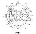
- a processor element (PE) 103 consisting of CMOS and the like
- necessary processing is performed in the PE 103.
- its output is supplied to another PE 103 through the electric wire 104 or optical path 105.
- the electric wire 104 transmits the signal in the same way as an ordinary IC.
- the optical directivity factor of the laser used in the second embodiment is high, and hence, the signal is transmitted only to a desired light-receiving device. For example, an optical signal emitted from the (001) face can be received only by the light-receiving device 102 on the (00-1) face as illustrated in Fig. 8.
- an optical signal emitted from the (100) face can be received only by the light-receiving device 102 on the (-100) face.
- the received signal is processed by the PE nearby, and transmitted through the electric wire 104 or optical wiring 105.
- electric wiring 104 and optical wiring 105 can be organically connected.
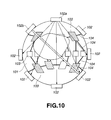
- Fig. 10 illustrates the third embodiment.
- reference numeral 102a is a light-emitting device for 1 ⁇ N optical wiring.
- an output from the PE can be converted into multiple outputs (i.e., fan-out).
- Reference numeral 102b is a light-emitting device for 1 ⁇ 1 optical wiring.
- 1 ⁇ 1 optical wiring can be achieved. In the 1 ⁇ 1 optical wiring, high speed data transfer can be achieved though flexibility of the wiring is somewhat lowered compared to the 1 ⁇ N optical wiring.
- an optical device whose consumption electric power is very small can be fabricated, since a light radiation layer of GaAsN series can be readily laid down on the Si ball.
Landscapes
- Physics & Mathematics (AREA)
- Engineering & Computer Science (AREA)
- Microelectronics & Electronic Packaging (AREA)
- General Physics & Mathematics (AREA)
- Optics & Photonics (AREA)
- Light Receiving Elements (AREA)
- Semiconductor Lasers (AREA)
- Led Devices (AREA)
- Photo Coupler, Interrupter, Optical-To-Optical Conversion Devices (AREA)
- Led Device Packages (AREA)
Abstract
Description
Claims (15)
- An optoelectric integrated device comprising:a three-dimensional solid semiconductor crystal; anda plurality of optical devices, including a light-emitting device and a light-receiving device, said optical devices being integrated on a surface of said semiconductor crystal,wherein light is emitted and received between said light-emitting device and said light-receiving device through an interior of said semiconductor crystal which is used as optical wiring medium.
- An optoelectric integrated device comprising:a silicon (Si) ball;a plurality of optical devices, including a light-emitting device and a light-receiving device, said light-emitting device having an oscillation wavelength longer than a bandgap wavelength of said Si ball; andan electronic device, said electronic device having at least one function selected from the group of switching on and off said light-emitting device, converting light received by said light-receiving device into an electric signal, and performing at least one arithmetic or logical operation on the basis of the electric signal, and said optical devices and said electronic device being integrated on a surface of said Si ball,wherein light is emitted and received between said light-emitting device and said light-receiving device through an interior of said Si ball which is used as optical wiring medium.
- An optoelectric integrated device comprising:a spherical semiconductor; andat least one of a light-emitting device for emitting signal light into an interior of said spherical semiconductor and a light-receiving device for receiving signal light transmitted through the interior of said spherical semiconductor.
- The optoelectric integrated device according to claim 1 or 3, further comprising an electronic device, wherein said semiconductor crystal comprises a silicon (Si) ball, and said electronic device and said optical devices are integrated on a surface of said Si ball.
- The optoelectric integrated device according to any one of claims 1 to 4, wherein said optical device includes a portion composed of III-VN semiconductor material or IV semiconductor material.
- The optoelectric integrated device according to claim 5, wherein said III-VN semiconductor material is selected from the group consisting of GaNAs, GaInNAs, AlNAs, and GaInNAsP.
- The optoelectric integrated device according to claim 5 or 6, wherein said IV semiconductor material is SiGe.
- The optoelectric integrated device according to any one of claims 1 to 7, further comprising a buffer layer for lattice matching which is formed on the surface of said semiconductor, wherein said optical devices are formed on said buffer layer.
- The optoelectric integrated device according to any one of claims 1 to 8, wherein said light-emitting device is constructed such that it emits spontaneous emission light or induced emission light into the interior of said semiconductor crystal, the light having a wavelength longer than a bandgap wavelength of said semiconductor crystal.
- The optoelectric integrated device according to any one of claims 1 to 9, wherein at least one said light-receiving device is arranged to receive the light emitted by said light-emitting device.
- The optoelectric integrated device according to any one of claims 1 to 10, wherein said light-emitting device is constructed such that it emits spontaneous emission light or induced emission light into an exterior of said semiconductor crystal.
- The optoelectric integrated device according to any one of claims 1 to 11, wherein said light-receiving device is arranged such that it receives light emitted into the interior of said semiconductor crystal by one or a plurality of said light-emitting devices.
- The optoelectric integrated device according to any one of claims 1 to 12, wherein said light-receiving device is arranged such that it receives light from an exterior of said semiconductor crystal.
- The optoelectric integrated device according to any one of claims 1 to 13, wherein said optical devices include plural such light-emitting devices and light-receiving devices, and wherein said light-emitting devices include a light-emitting device which can emit light into the interior of said semiconductor crystal toward a predetermined one of said light-receiving devices, and a light-emitting device which can emit light into the interior of said semiconductor crystal toward a plurality of predetermined ones of said light-receiving devices.
- The optoelectric integrated device according to any one of claims 1 and 3 to 14, further comprising an electronic device formed on the surface of said semiconductor crystal, said electronic device having at least one function selected from the group of switching on and off said light-emitting device, converting light received by said light-receiving device into an electric signal, and performing at least one arithmetic or logical operation on the basis of the electric signal.
Applications Claiming Priority (2)
| Application Number | Priority Date | Filing Date | Title |
|---|---|---|---|
| JP2000090826 | 2000-03-29 | ||
| JP2000090826A JP3689615B2 (en) | 2000-03-29 | 2000-03-29 | Photoelectric fusion device having a three-dimensional shape |
Publications (2)
| Publication Number | Publication Date |
|---|---|
| EP1139122A2 true EP1139122A2 (en) | 2001-10-04 |
| EP1139122A3 EP1139122A3 (en) | 2005-01-12 |
Family
ID=18606377
Family Applications (1)
| Application Number | Title | Priority Date | Filing Date |
|---|---|---|---|
| EP01107915A Withdrawn EP1139122A3 (en) | 2000-03-29 | 2001-03-28 | Optoelectric integrated device having a three-dimensional solid configuration |
Country Status (3)
| Country | Link |
|---|---|
| US (1) | US6563137B2 (en) |
| EP (1) | EP1139122A3 (en) |
| JP (1) | JP3689615B2 (en) |
Cited By (3)
| Publication number | Priority date | Publication date | Assignee | Title |
|---|---|---|---|---|
| EP1219994A3 (en) * | 2000-12-28 | 2004-11-10 | Canon Kabushiki Kaisha | Semiconductor device, optoelectronic board, and production methods therefor |
| US6819813B2 (en) | 2002-09-11 | 2004-11-16 | International Business Machines Corporation | Optical land grid array interposer |
| EP1496381A3 (en) * | 2003-07-01 | 2008-02-06 | Matsushita Electric Industrial Co., Ltd. | Mount assembly, optical transmission line and photoelectric circuit board |
Families Citing this family (16)
| Publication number | Priority date | Publication date | Assignee | Title |
|---|---|---|---|---|
| JP3890999B2 (en) * | 2002-02-14 | 2007-03-07 | 住友電気工業株式会社 | Optical transmission module |
| JP3927883B2 (en) | 2002-08-02 | 2007-06-13 | キヤノン株式会社 | Optical waveguide device and photoelectric fusion substrate using the same |
| JP3897688B2 (en) * | 2002-12-11 | 2007-03-28 | キヤノン株式会社 | Optoelectronic wiring board |
| WO2005055285A2 (en) * | 2003-12-01 | 2005-06-16 | The Regents Of The University Of California | Multiband semiconductor compositions for photovoltaic devices |
| US9524869B2 (en) | 2004-03-11 | 2016-12-20 | Epistar Corporation | Nitride-based semiconductor light-emitting device |
| US8562738B2 (en) | 2004-03-11 | 2013-10-22 | Epistar Corporation | Nitride-based light-emitting device |
| US7928424B2 (en) * | 2004-03-11 | 2011-04-19 | Epistar Corporation | Nitride-based light-emitting device |
| JP4019285B2 (en) * | 2005-02-04 | 2007-12-12 | セイコーエプソン株式会社 | Surface emitting device and method for manufacturing the same |
| JP4019284B2 (en) * | 2005-02-04 | 2007-12-12 | セイコーエプソン株式会社 | Surface emitting device and method for manufacturing the same |
| CA2547489C (en) * | 2005-05-18 | 2011-06-14 | Ecovu Analytics Inc. | Fluid contamination analyzer and sample cell therefor |
| US8338186B2 (en) * | 2005-05-18 | 2012-12-25 | Ecovu Analytics Inc. | Method and system for fluid purification and analysis |
| US20070082505A1 (en) * | 2005-10-11 | 2007-04-12 | Freescale Semiconductor, Inc. | Method of forming an electrically insulating layer on a compound semiconductor |
| US7531371B2 (en) * | 2006-02-21 | 2009-05-12 | Rather John D G | Multisurfaced microdevice system array and a method of producing the array |
| JP2007234724A (en) * | 2006-02-28 | 2007-09-13 | Canon Inc | Vertical cavity surface emitting laser and method for producing two-dimensional photonic crystal in vertical cavity surface emitting laser |
| JP4973940B2 (en) * | 2007-10-15 | 2012-07-11 | ソニー株式会社 | Manufacturing method of semiconductor light emitting device |
| JP4215812B1 (en) | 2008-02-27 | 2009-01-28 | 国立大学法人広島大学 | Optical integrated circuit device |
Family Cites Families (11)
| Publication number | Priority date | Publication date | Assignee | Title |
|---|---|---|---|---|
| US5200631A (en) * | 1991-08-06 | 1993-04-06 | International Business Machines Corporation | High speed optical interconnect |
| JP3194503B2 (en) | 1992-06-04 | 2001-07-30 | キヤノン株式会社 | Compound semiconductor device and method of manufacturing the same |
| US5937274A (en) * | 1995-01-31 | 1999-08-10 | Hitachi, Ltd. | Fabrication method for AlGaIn NPAsSb based devices |
| US5955776A (en) * | 1996-12-04 | 1999-09-21 | Ball Semiconductor, Inc. | Spherical shaped semiconductor integrated circuit |
| US6097472A (en) | 1997-04-17 | 2000-08-01 | Canon Kabushiki Kaisha | Apparatus and method for exposing a pattern on a ball-like device material |
| JPH1154406A (en) | 1997-08-04 | 1999-02-26 | Mitsui High Tec Inc | Method for exposing spheric ic |
| JPH11161766A (en) * | 1997-11-28 | 1999-06-18 | Mitsui High Tec Inc | Ic card |
| US6052517A (en) * | 1998-06-30 | 2000-04-18 | Ball Semiconductor, Inc. | Spherical cell design for VLSI circuit design on a spherical semiconductor |
| JP3865944B2 (en) * | 1998-07-23 | 2007-01-10 | Ntn株式会社 | Silicon ball manufacturing method and apparatus |
| JP4054480B2 (en) | 1999-05-18 | 2008-02-27 | キヤノン株式会社 | Photoelectric fusion device structure on Si substrate, manufacturing method thereof, and film forming method |
| US6423974B1 (en) * | 1999-05-28 | 2002-07-23 | Ball Semiconductor, Inc. | X-ray imaging apparatus using spherical semiconductor detectors |
-
2000
- 2000-03-29 JP JP2000090826A patent/JP3689615B2/en not_active Expired - Fee Related
-
2001
- 2001-03-27 US US09/817,344 patent/US6563137B2/en not_active Expired - Fee Related
- 2001-03-28 EP EP01107915A patent/EP1139122A3/en not_active Withdrawn
Cited By (6)
| Publication number | Priority date | Publication date | Assignee | Title |
|---|---|---|---|---|
| EP1219994A3 (en) * | 2000-12-28 | 2004-11-10 | Canon Kabushiki Kaisha | Semiconductor device, optoelectronic board, and production methods therefor |
| US6897430B2 (en) | 2000-12-28 | 2005-05-24 | Canon Kabushiki Kaisha | Semiconductor device, optoelectronic board, and production methods therefor |
| US6936808B2 (en) | 2000-12-28 | 2005-08-30 | Canon Kabushiki Kaisha | Semiconductor device, optoelectronic board, and production methods therefor |
| US7141778B2 (en) | 2000-12-28 | 2006-11-28 | Canon Kabushiki Kaisha | Semiconductor device, optoelectronic board, and production methods therefor |
| US6819813B2 (en) | 2002-09-11 | 2004-11-16 | International Business Machines Corporation | Optical land grid array interposer |
| EP1496381A3 (en) * | 2003-07-01 | 2008-02-06 | Matsushita Electric Industrial Co., Ltd. | Mount assembly, optical transmission line and photoelectric circuit board |
Also Published As
| Publication number | Publication date |
|---|---|
| US20010032984A1 (en) | 2001-10-25 |
| US6563137B2 (en) | 2003-05-13 |
| JP3689615B2 (en) | 2005-08-31 |
| EP1139122A3 (en) | 2005-01-12 |
| JP2001284635A (en) | 2001-10-12 |
Similar Documents
| Publication | Publication Date | Title |
|---|---|---|
| US6563137B2 (en) | Optoelectric integrated device having a three-dimensional solid configuration | |
| US5357122A (en) | Three-dimensional optical-electronic integrated circuit device with raised sections | |
| US5633527A (en) | Unitary lens semiconductor device | |
| US5861636A (en) | Surface emitting visible light emiting diode having ring-shaped electrode | |
| Delbeke et al. | High-efficiency semiconductor resonant-cavity light-emitting diodes: a review | |
| US6261859B1 (en) | Method for fabricating surface-emitting semiconductor device, surface-emitting semiconductor device fabricated by the method, and display device using the device | |
| US7787511B2 (en) | Array of surface-emitting laser diodes having reduced device resistance and capable of performing high output operation and method of fabricating the surface-emitting laser diode | |
| US7680162B2 (en) | Long wavelength vertical cavity surface emitting laser device and method of fabricating the same | |
| EP1026798B1 (en) | Vertical cavity surface emitting laser (VCSEL), using buried bragg reflectors and method for producing same | |
| JPH05218386A (en) | Optical integrated circuit | |
| US5665985A (en) | Light-emitting diode of edge-emitting type, light-receiving device of lateral-surface-receiving type, and arrayed light source | |
| CN104769467A (en) | Semiconductor device | |
| JPH0555703A (en) | Plane emission laser device | |
| US20240332901A1 (en) | Surface-emitting semiconductor laser and method for producing a surface-emitting semiconductor laser | |
| CN115298917A (en) | Light-emitting element, light-emitting element unit, electronic device, light-emitting device, sensing device, and communication device | |
| JP2002141612A (en) | Micro lens integrated surface light laser | |
| US6277668B1 (en) | Optical detector for minimizing optical crosstalk | |
| KR100413708B1 (en) | Microcavity LED photon recycling | |
| JP7593332B2 (en) | Light emitting device, its manufacturing method, and light emitting device array | |
| US7406112B2 (en) | Surface-emitting laser, method for manufacturing surface-emitting laser, device and electronic apparatus | |
| US20090129426A1 (en) | Semiconductor System Having a Ring Laser Fabricated by Epitaxial Layer Overgrowth | |
| US20070166961A1 (en) | Fabrication method of semiconductor luminescent device | |
| JP2002252418A (en) | Optical communication system | |
| US20030123509A1 (en) | Semiconductor laser based on matrix, array or single triangle optical cavity with spatially distributed current injection | |
| EP1221725A1 (en) | Highly efficient paraboloid light emitting diode |
Legal Events
| Date | Code | Title | Description |
|---|---|---|---|
| PUAI | Public reference made under article 153(3) epc to a published international application that has entered the european phase |
Free format text: ORIGINAL CODE: 0009012 |
|
| AK | Designated contracting states |
Kind code of ref document: A2 Designated state(s): AT BE CH CY DE DK ES FI FR GB GR IE IT LI LU MC NL PT SE TR |
|
| AX | Request for extension of the european patent |
Free format text: AL;LT;LV;MK;RO;SI |
|
| PUAL | Search report despatched |
Free format text: ORIGINAL CODE: 0009013 |
|
| AK | Designated contracting states |
Kind code of ref document: A3 Designated state(s): AT BE CH CY DE DK ES FI FR GB GR IE IT LI LU MC NL PT SE TR |
|
| AX | Request for extension of the european patent |
Extension state: AL LT LV MK RO SI |
|
| 17P | Request for examination filed |
Effective date: 20050711 |
|
| AKX | Designation fees paid |
Designated state(s): DE FR GB |
|
| STAA | Information on the status of an ep patent application or granted ep patent |
Free format text: STATUS: THE APPLICATION HAS BEEN WITHDRAWN |
|
| 18W | Application withdrawn |
Effective date: 20101015 |