EP1137277A2 - Image displaying method and apparatus - Google Patents
Image displaying method and apparatus Download PDFInfo
- Publication number
- EP1137277A2 EP1137277A2 EP01300454A EP01300454A EP1137277A2 EP 1137277 A2 EP1137277 A2 EP 1137277A2 EP 01300454 A EP01300454 A EP 01300454A EP 01300454 A EP01300454 A EP 01300454A EP 1137277 A2 EP1137277 A2 EP 1137277A2
- Authority
- EP
- European Patent Office
- Prior art keywords
- image signal
- horizontal
- period
- horizontal line
- image
- Prior art date
- Legal status (The legal status is an assumption and is not a legal conclusion. Google has not performed a legal analysis and makes no representation as to the accuracy of the status listed.)
- Withdrawn
Links
Images




Classifications
-
- H—ELECTRICITY
- H04—ELECTRIC COMMUNICATION TECHNIQUE
- H04N—PICTORIAL COMMUNICATION, e.g. TELEVISION
- H04N5/00—Details of television systems
- H04N5/74—Projection arrangements for image reproduction, e.g. using eidophor
- H04N5/7416—Projection arrangements for image reproduction, e.g. using eidophor involving the use of a spatial light modulator, e.g. a light valve, controlled by a video signal
Definitions
- the present invention relates to a method and apparatus for displaying an image signal such as a television signal, and more particularly to an image displaying method and apparatus capable of displaying an image at a high luminance.
- One horizontal period of a television signal has a horizontal image signal period and a horizontal blanking period.
- one horizontal scanning period (T H ) is divided into five periods each having a time equal to the horizontal blanking time (T BLK ).
- the four periods are effective display periods of image signals.
- Target pixels in the horizontal direction are divided into four groups of pixels and electron beams are sequentially supplied to the pixels in each group.
- image signals in each divided group cannot be converted into parallel signals unless all image signals in the divided group are read. Therefore, the parallel signals converted from image signals in each divided period are output and displayed during the next divided period. Specifically, the image signals corresponding to the periods T 1 , T 2 , T 3 and T 4 are converted into parallel signals and output and displayed at the same time during the first to fourth quarter division periods of a target scan line.
- the image signals corresponding to the period T 4 can be displayed by utilizing the period corresponding to the period T BLK , the image signals cannot be displayed during the period corresponding to the period T 1 after the period T BLK , because no image signals exist during this period T BLK . Therefore, only one fifth of one horizontal scanning time T H is used for displaying image signals and it can be said that the method is unsatisfactory from the viewpoint of high luminance.
- the invention provides an image displaying method of displaying an image signal having a horizontal image signal period and a horizontal blanking period, the method comprising the steps of: (a) writing a first horizontal line image signal in a write memory; (b) reading in parallel the first horizontal line image signal from a read memory during a horizontal blanking period next to the horizontal image signal period; (c) amplifying the first horizontal line image signal to thereafter perform modulation; (d) displaying the first horizontal line image signal at least until a next horizontal image signal line period terminates; and (e) sequentially repeating the steps (a) to (d) to scan horizontal lines.
- an image display apparatus for displaying an image signal, comprising: a linear optical deflector having optical deflectors for pixels in a horizontal direction, one horizontal line image signal being displayed at the same time by modulating in parallel the linear optical deflector.
- Fig. 1 is a diagram showing an example of an image signal used by an image displaying method according to an embodiment of the invention.
- Fig. 2 is a block diagram showing a driver circuit illustrating the image displaying method of the embodiment.
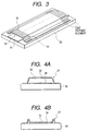
- Fig. 3 is a schematic perspective view showing an example of the structure of a reflection type diffraction grating suitable for use with an image displaying apparatus according to an embodiment of the invention.
- Figs. 4A and 4B are diagrams illustrating deformation of a striped element of the diffraction grating shown in Fig. 3.
- Fig. 5 is a cross sectional view illustrating modulation by the diffraction grating shown in Fig. 3 the cross sectional view being taken along a scan line.
- Fig. 6 is a cross sectional view illustrating modulation by the diffraction grating shown in Fig. 3 the cross sectional view being taken along the scan line.
- Fig. 7 is a graph showing the characteristics of applied voltage and reflected light intensity of a diffraction grating suitable for use with the image displaying apparatus of the invention.
- Fig. 8 is a schematic diagram showing an example of the structure of the image displaying apparatus.
- Fig. 9 is a diagram explaining conventional techniques.
- An image displaying method uses an image signal whose one horizontal period T H has as shown in Fig. 1 a horizontal image signal period T V (e.g., 50 ⁇ sec) and a horizontal blanking period T BLK (e.g., 12.7 ⁇ sec).
- Such image signals are displayed as each horizontal line image signal at the same time by using a driver circuit such as shown in the block diagram of Fig. 2.
- reference numeral 1 represents a write memory for writing image signals same in number as the number of pixels in one horizontal line (i.e., one horizontal line image signal).
- Reference numeral 2 represents a read memory for reading the image signals. These memories 1 and 2 are made of, for example, sample/hold circuits and convert sequentialy image signals into parallel image signals.
- Reference numeral 3 represents an amplifier, reference numeral 4 represents a modulator, and reference numeral 5 represents an image display plane.
- a first horizontal line image signal V TV1 is written in the memory 1 during a first horizontal image signal period T V1 .
- This first horizontal line image signal V TV1 is read to the memory 2 during the horizontal blanking period T BLK2 following the first horizontal image signal period T V1 , and amplified by the amplifier 3.
- the amplified signal drives the modulator 4 and an image is displayed on the image display plane 5 at least until a second horizontal image signal period T V2 terminates.
- a second horizontal line image signal V TV2 is written in the memory 1. The above operations are repeated to scan all horizontal lines.
- each horizontal line image signal starts being displayed at the timing in the next horizontal blanking period and continues to be displayed at least until the next horizontal image signal period is terminated. Therefore, each pixel is driven at the maximum during one horizontal period and a high luminance can be realized.
- the display start timing is not limited in particular, but it may be any timing so long as it is during the next horizontal blanking period, such as a start timing of the horizontal blanking period and any other timing.
- the longer the display period the luminance becomes higher. Therefore, it is preferable to display during the full one horizontal period. For example, if the display starts at the middle of the horizontal blanking period, the display is made to continue to the middle of the next horizontal blanking period.
- the modulator 4 may have the structure that an electron beam or the like output from an electron source or the like is modulated by a control electrode group or the like, similar to that described in Japanese Patent Publication No. 61-26271.
- the image displaying method according to the embodiment of the invention is particularly effective if light is used as a pixel illumination source which light is relatively difficult to obtain a high luminance. If light is used as a pixel illumination source, for example, a linear light deflector having light deflectors for pixels in the horizontal direction is suitable for the modulator 4.
- Such a light deflector may be made of bimetal, mirror, reflection type diffraction grating or the like.
- a reflection type diffraction grating having a high speed response such as shown in Fig. 3 is suitable for use with the image displaying apparatus.
- Fig. 3 is a perspective view of a reflection type diffraction grating suitable for use with the image displaying apparatus according to an embodiment of the invention.
- This reflection type diffraction grating is made of a light modulator having striped elements 31 disposed in a linear array on a substrate 30.
- the striped element 31 is made of a thin film capable of being deformed in concave and convex shapes. Four striped elements 31 correspond to one pixel, and the striped elements 31 corresponding in number to the number of pixels in the horizontal direction are provided.
- the material of the substrate 30 may be silicon or the like.
- a passivation layer (not shown) of silicon nitride (Si 3 N 4 ) or the like is formed on the substrate 30.
- a conductive layer 34 made of tungsten or tungsten alloy is formed on this passivation layer.
- the striped element 31 is made of silicon nitride or the like. Opposite end portions of the striped element 31 are fixed to the substrate 30 at positions away from the conductive layer 34. A flat element portion 32 at the middle of the striped element 31 is spaced from the substrate 30 to form an air gap 33 therebetween. The upper surface of the striped element 31 is covered with light reflecting material such as an aluminum film.
- the height of the air gap 33 can be controlled by a voltage applied between the striped element 31 and conductive layer 34.
- a voltage is not applied, the striped element 31 takes a convex shape such as shown in Fig. 4A.
- the striped element 31 is deformed by electrostatic attraction and the flat element portion 32 is bent toward the substrate 30 and contacts the substrate 30.
- the striped elements 31 When all of the striped elements 31 are in the convex shape as shown in Fig. 4A, if light of wavelength ⁇ is incident perpendicularly in a surface of the substrate 30, light reflected from the flat element portions 32 has the same phase, as shown in Fig. 5. Therefore, the striped elements function as a flat mirror.
- the striped elements 31 have alternately the convex and concave shapes (the height difference between the convex and concave shapes is preferably 1/4 ⁇ )
- the light of a wavelength ⁇ is incident perpendicularly in the surface of the substrate 30, the phase of light reflected from the convex surface shifts greatly from the phase of light reflected from the concave surface, as shown in Fig. 6. Therefore, interference occurs between these lights reflected from the convex and concave.
- the light is reflected at an angle ⁇ relative to the directions normal to the substrate.
- the pixel does not receive the light from four striped elements 31 corresponding to the pixel by modulating them as shown in Fig. 5. Thus, this pixel can be displayed as a dark pixel. While the pixel receives light from four striped elements 31 corresponding to the pixel by modulating them as shown in Fig. 6. Thus, this pixel can be displayed as a bright pixel.
- the light deflection angle ⁇ is determined by the width of the striped element, the space between adjacent striped elements and the like. It is preferable that the width of the striped element is set to about 3.5 ⁇ m and that the space between adjacent striped elements is desirably minimized in order to reduce a light loss in the space.
- Fig. 7 is a graph showing an example of the characteristics of applied voltage and reflected light intensity of the reflection type diffraction grating having the above-described structure.
- the light deflector using the above-described reflection type diffraction grating has a very short response period, typically about 20 nsec. Modulation is preferably made by using voltage pulses. By controlling the width and amplitude of a voltage pulse, the luminance at the image display plane can be controlled and gradation display can be made.
- Fig. 8 shows an example of an image display apparatus having the above-described linear optical deflector according to an embodiment of the invention.
- Reference numeral 101 represents a linear optical deflector (reflection type diffraction grating) such as shown in Fig. 3, reference numeral 102 represents a light source, reference numeral 103 represents a lens, reference numeral 108 represents a half mirror, reference numeral 109 represents a projector lens, reference numeral 110 represents a stopper, and a reference numeral 111 represents a deflector (galvano mirror).
- reference numeral 101 represents a linear optical deflector (reflection type diffraction grating) such as shown in Fig. 3
- reference numeral 102 represents a light source
- reference numeral 103 represents a lens
- reference numeral 108 represents a half mirror
- reference numeral 109 represents a projector lens
- reference numeral 110 represents a stopper
- a reference numeral 111 represents a deflector (galvano mirror).
- Light emitted from the light source 102 is converted into parallel light fluxes by the lens 103, reflected by the half mirror 108, and becomes incident upon the reflection type diffraction grating 101.
- Modulation signals (voltage pulses) read in parallel from the memory 2 and amplified by the amplifier 3 are applied to the striped elements 31 of the reflection type diffraction grating 101 to modulate the striped elements in accordance with the luminance of each pixel in the horizontal direction.
- incident light 104 propagates reversely along the incidence optical path and transmits through the half mirror 108.
- This transmitted light beam 107 is converged as a light beam 113 upon the focal point of the projector lens 109 and absorbed by the stopper 110.
- the image displaying apparatus of this invention uses, as the pixel illuminating source for the image display plane, light instead of an electron beam which light is relatively difficult to obtain a high luminance.
- one horizontal line image signal is displayed at the same time by modulating in parallel the linear optical deflector 101 having optical deflectors for pixels in the horizontal direction and the image displaying method of this invention can be applied.
- Each pixel can be driven at the maximum during one horizontal period and a high luminance can be realized.
- a color image displaying apparatus can be realized by using red, green and blue light sources as the light source 102. Specifically, if red is to be displayed, a voltage pulse to be applied between the striped element 31 and conductive layer 34 is controlled so as to realize a diffraction grating capable of diffracting red light at an angle ⁇ .
- displaying of the first horizontal line image signal starts during the timing in the horizontal blanking period next to the horizontal image signal period, and continues at least until termination of the next second horizontal line image signal period. It is therefore possible to drive each pixel at the maximum during one horizontal period and realize a high luminance. A high luminance can be realized even if light which is relatively difficult to obtain a high luminance is used as the pixel exposure source, by displaying at the same time one horizontal line image signal by modulating in parallel a linear optical deflector.
- modulation can be made easily by using voltage pulses and gradation display is possible by controlling the width and/or amplitude of the voltage pulse.
- the image displaying apparatus of this invention uses, as the pixel illuminating source for the image display plane, light instead of an electron beam which light is relatively difficult to obtain a high luminance.
- one horizontal line image signal is displayed at the same time by modulating in parallel the linear optical deflector having optical deflectors for pixels in the horizontal direction and the image displaying method of this invention can be applied.
- Each pixel can be driven at the maximum during one horizontal period and a high luminance can be realized.
Landscapes
- Engineering & Computer Science (AREA)
- Multimedia (AREA)
- Signal Processing (AREA)
- Control Of Indicators Other Than Cathode Ray Tubes (AREA)
- Transforming Electric Information Into Light Information (AREA)
- Mechanical Light Control Or Optical Switches (AREA)
Abstract
Description
Claims (10)
- An image displaying method of displaying an image signal having a horizontal image signal period and a horizontal blanking period, the method comprising the steps of:(a) writing a first horizontal line image signal in a write memory;(b) reading in parallel the first horizontal line image signal from a read memory during a horizontal blanking period next to the horizontal image signal period;(c) amplifying the first horizontal line image signal to thereafter perform modulation;(d) displaying the first horizontal line image signal at least until a next horizontal image signal line period terminates; and(e) sequentially repeating said steps (a) to (d) to scan horizontal lines.
- An image displaying method according to claim 1, wherein a light source is used as source for illuminating an image display plane, and the modulation of the first horizontal line image signal is performed by modulating in parallel a linear optical deflector having optical deflectors for the pixels in a horizontal direction.
- An image displaying method according to claim 2, wherein the linear optical deflector is a reflection type diffraction grating having striped elements disposed in a linear array on a substrate, the striped element being capable of deforming in convex and concave shapes.
- An image displaying method according to claim 3, wherein modulation of the reflection type diffraction grating is performed by applying voltage pulses.
- An image displaying method according to claim 4, wherein gradation display is performed by controlling a width and/or amplitude of the voltage pulse.
- An image display apparatus for displaying an image signal, comprising:
a linear optical deflector having optical deflectors for pixels in a horizontal direction, one horizontal line image signal being displayed at the same time by modulating in parallel the linear optical deflector. - An image display apparatus according to claim 6, wherein the optical deflector is a reflection type diffraction grating having striped elements disposed in a linear array on a substrate, the striped elements being capable of deforming in convex and concave shapes.
- An apparatus according to claim 6 or claim 7 comprising:means for writing a first horizontal line image signal in a write memory;means for reading in parallel the first horizontal line image signal from a read memory during a horizontal blanking period next to the horizontal image signal period;means for amplifying the first horizontal line image signal to thereafter perform modulation;and means for displaying the first horizontal line image signal at least until the next horizontal image signal line period terminates.
- Apparatus according to claim 8, and further including a light source which in operation directs light onto a semi-reflecting mirror in the optical path between the diffraction grating and a display plane.
- Apparatus according to any one of claims 6 to 9 wherein the light source is a multi-colour light source.
Applications Claiming Priority (2)
| Application Number | Priority Date | Filing Date | Title |
|---|---|---|---|
| JP2000011164 | 2000-01-20 | ||
| JP2000011164 | 2000-01-20 |
Publications (2)
| Publication Number | Publication Date |
|---|---|
| EP1137277A2 true EP1137277A2 (en) | 2001-09-26 |
| EP1137277A3 EP1137277A3 (en) | 2005-03-09 |
Family
ID=18539066
Family Applications (1)
| Application Number | Title | Priority Date | Filing Date |
|---|---|---|---|
| EP01300454A Withdrawn EP1137277A3 (en) | 2000-01-20 | 2001-01-19 | Image displaying method and apparatus |
Country Status (2)
| Country | Link |
|---|---|
| US (1) | US6608621B2 (en) |
| EP (1) | EP1137277A3 (en) |
Cited By (1)
| Publication number | Priority date | Publication date | Assignee | Title |
|---|---|---|---|---|
| EP1454186A4 (en) * | 2001-11-30 | 2006-01-18 | Silicon Light Machines Inc | Display apparatus including rgb color combiner and 1d light valve relay including schlieren filter |
Families Citing this family (1)
| Publication number | Priority date | Publication date | Assignee | Title |
|---|---|---|---|---|
| JP2002006241A (en) * | 2000-06-19 | 2002-01-09 | Sony Corp | Optical switching element, switching device using the same, and image display device |
Family Cites Families (22)
| Publication number | Priority date | Publication date | Assignee | Title |
|---|---|---|---|---|
| JPS54109722A (en) * | 1978-02-16 | 1979-08-28 | Sony Corp | Flat-type picture display device |
| US4441791A (en) * | 1980-09-02 | 1984-04-10 | Texas Instruments Incorporated | Deformable mirror light modulator |
| US4571603A (en) * | 1981-11-03 | 1986-02-18 | Texas Instruments Incorporated | Deformable mirror electrostatic printer |
| JPS60264194A (en) * | 1984-06-12 | 1985-12-27 | Nec Home Electronics Ltd | Method for processing stereoscopic television signal and equipment at its transmission and reception side |
| JPH0658977B2 (en) | 1984-07-16 | 1994-08-03 | 株式会社小糸製作所 | Semiconductor element |
| JP2823156B2 (en) | 1985-07-23 | 1998-11-11 | キヤノン株式会社 | Display device |
| US5299042A (en) * | 1990-05-30 | 1994-03-29 | Victor Company Of Japan, Ltd. | Light-to-light conversion method, display unit using the same, and light-to-light conversion element incorporated therein |
| DE69113150T2 (en) * | 1990-06-29 | 1996-04-04 | Texas Instruments Inc | Deformable mirror device with updated grid. |
| US5191624A (en) * | 1990-09-19 | 1993-03-02 | Hitachi, Ltd. | Optical information storing apparatus and method for production of optical deflector |
| DE69213357T2 (en) * | 1991-06-27 | 1997-01-16 | Texas Instruments Inc | Modulation method for deformable mirror device (DMD) |
| JPH05210085A (en) * | 1992-01-30 | 1993-08-20 | Canon Inc | Display controller |
| US6040937A (en) * | 1994-05-05 | 2000-03-21 | Etalon, Inc. | Interferometric modulation |
| JPH0811347A (en) * | 1994-07-04 | 1996-01-16 | Fuji Xerox Co Ltd | Pixel clock generator |
| KR0149215B1 (en) * | 1994-11-11 | 1998-10-15 | 배순훈 | Pixel driving circuit |
| US5668611A (en) * | 1994-12-21 | 1997-09-16 | Hughes Electronics | Full color sequential image projection system incorporating pulse rate modulated illumination |
| US5684621A (en) * | 1995-05-08 | 1997-11-04 | Downing; Elizabeth Anne | Method and system for three-dimensional display of information based on two-photon upconversion |
| US5587742A (en) * | 1995-08-25 | 1996-12-24 | Panasonic Technologies, Inc. | Flexible parallel processing architecture for video resizing |
| JP2991097B2 (en) * | 1995-12-20 | 1999-12-20 | 富士ゼロックス株式会社 | Image forming device |
| US20020057349A1 (en) * | 1996-03-06 | 2002-05-16 | Masanori Yamaguchi | Image pickup apparatus and solid state image pickup device |
| US5982553A (en) * | 1997-03-20 | 1999-11-09 | Silicon Light Machines | Display device incorporating one-dimensional grating light-valve array |
| JP3865942B2 (en) * | 1998-07-17 | 2007-01-10 | 富士フイルムホールディングス株式会社 | Active matrix element, light emitting element using the active matrix element, light modulation element, light detection element, exposure element, display device |
| US6449084B1 (en) * | 1999-05-10 | 2002-09-10 | Yanping Guo | Optical deflector |
-
2001
- 2001-01-17 US US09/760,703 patent/US6608621B2/en not_active Expired - Fee Related
- 2001-01-19 EP EP01300454A patent/EP1137277A3/en not_active Withdrawn
Cited By (1)
| Publication number | Priority date | Publication date | Assignee | Title |
|---|---|---|---|---|
| EP1454186A4 (en) * | 2001-11-30 | 2006-01-18 | Silicon Light Machines Inc | Display apparatus including rgb color combiner and 1d light valve relay including schlieren filter |
Also Published As
| Publication number | Publication date |
|---|---|
| EP1137277A3 (en) | 2005-03-09 |
| US20010050727A1 (en) | 2001-12-13 |
| US6608621B2 (en) | 2003-08-19 |
Similar Documents
| Publication | Publication Date | Title |
|---|---|---|
| AU648762B2 (en) | Television with apertures to modulate beam intensity | |
| US5126836A (en) | Actuated mirror optical intensity modulation | |
| AU661501B2 (en) | Membrane light modulating systems | |
| EP0547601B1 (en) | Color display system using spatial light modulators | |
| US7891818B2 (en) | System and method for aligning RGB light in a single modulator projector | |
| EP1977413A2 (en) | Optical designs for scanning beam display systems using fluorescent screens | |
| EP1285769B1 (en) | Method and apparatus for printing high resolution images using multiple reflective spatial light modulators | |
| US8040332B2 (en) | Light scan device and image display device | |
| US6020940A (en) | Liquid crystal projector and method of driving the projector | |
| US7075562B2 (en) | Optical scanning device | |
| US7593151B2 (en) | Display unit and scanning method therefor | |
| US6608621B2 (en) | Image displaying method and apparatus | |
| JP2002055296A (en) | Optical scanning device and projection display device using the same | |
| US5777781A (en) | Optical projection system | |
| KR100498223B1 (en) | Optical modulation element and projection apparatus | |
| US6052229A (en) | Image display system using a thin-film actuated mirror array | |
| JP4042558B2 (en) | projector | |
| JP2001272952A (en) | Image display method and image display device | |
| KR100464300B1 (en) | Laser projection systm | |
| JP2004233524A (en) | projector | |
| JP3224433B2 (en) | Display device | |
| JP2709070B2 (en) | Image forming device | |
| JP2001083601A (en) | Projector device | |
| JPH0321924A (en) | Large screen display device | |
| CA2321760A1 (en) | Image display system using a thin-film actuated mirror array |
Legal Events
| Date | Code | Title | Description |
|---|---|---|---|
| PUAI | Public reference made under article 153(3) epc to a published international application that has entered the european phase |
Free format text: ORIGINAL CODE: 0009012 |
|
| AK | Designated contracting states |
Kind code of ref document: A2 Designated state(s): AT BE CH CY DE DK ES FI FR GB GR IE IT LI LU MC NL PT SE TR |
|
| AX | Request for extension of the european patent |
Free format text: AL;LT;LV;MK;RO;SI |
|
| PUAL | Search report despatched |
Free format text: ORIGINAL CODE: 0009013 |
|
| AK | Designated contracting states |
Kind code of ref document: A3 Designated state(s): AT BE CH CY DE DK ES FI FR GB GR IE IT LI LU MC NL PT SE TR |
|
| AX | Request for extension of the european patent |
Extension state: AL LT LV MK RO SI |
|
| 17P | Request for examination filed |
Effective date: 20050725 |
|
| AKX | Designation fees paid |
Designated state(s): DE FR GB |
|
| 17Q | First examination report despatched |
Effective date: 20080701 |
|
| STAA | Information on the status of an ep patent application or granted ep patent |
Free format text: STATUS: THE APPLICATION HAS BEEN WITHDRAWN |
|
| 18W | Application withdrawn |
Effective date: 20081029 |