EP1137174A2 - Automatic gain control system - Google Patents
Automatic gain control system Download PDFInfo
- Publication number
- EP1137174A2 EP1137174A2 EP01107267A EP01107267A EP1137174A2 EP 1137174 A2 EP1137174 A2 EP 1137174A2 EP 01107267 A EP01107267 A EP 01107267A EP 01107267 A EP01107267 A EP 01107267A EP 1137174 A2 EP1137174 A2 EP 1137174A2
- Authority
- EP
- European Patent Office
- Prior art keywords
- signal
- unit
- base
- band
- output
- Prior art date
- Legal status (The legal status is an assumption and is not a legal conclusion. Google has not performed a legal analysis and makes no representation as to the accuracy of the status listed.)
- Withdrawn
Links
- 238000001514 detection method Methods 0.000 claims abstract description 35
- 230000006866 deterioration Effects 0.000 claims abstract description 13
- 230000005540 biological transmission Effects 0.000 claims description 51
- 238000012935 Averaging Methods 0.000 claims description 22
- 238000006243 chemical reaction Methods 0.000 claims description 20
- 230000002194 synthesizing effect Effects 0.000 claims description 2
- 238000010586 diagram Methods 0.000 description 20
- 238000000034 method Methods 0.000 description 17
- 230000008878 coupling Effects 0.000 description 7
- 238000010168 coupling process Methods 0.000 description 7
- 238000005859 coupling reaction Methods 0.000 description 7
- 239000003990 capacitor Substances 0.000 description 6
- 238000012805 post-processing Methods 0.000 description 6
- 238000012937 correction Methods 0.000 description 4
- 238000012545 processing Methods 0.000 description 4
- 238000010295 mobile communication Methods 0.000 description 3
- 238000012546 transfer Methods 0.000 description 2
- 238000004891 communication Methods 0.000 description 1
- 230000003247 decreasing effect Effects 0.000 description 1
- 238000007599 discharging Methods 0.000 description 1
- 230000007274 generation of a signal involved in cell-cell signaling Effects 0.000 description 1
- 238000009499 grossing Methods 0.000 description 1
- 238000001228 spectrum Methods 0.000 description 1
Images




Classifications
-
- H—ELECTRICITY
- H03—ELECTRONIC CIRCUITRY
- H03G—CONTROL OF AMPLIFICATION
- H03G3/00—Gain control in amplifiers or frequency changers
- H03G3/20—Automatic control
- H03G3/30—Automatic control in amplifiers having semiconductor devices
- H03G3/3036—Automatic control in amplifiers having semiconductor devices in high-frequency amplifiers or in frequency-changers
- H03G3/3042—Automatic control in amplifiers having semiconductor devices in high-frequency amplifiers or in frequency-changers in modulators, frequency-changers, transmitters or power amplifiers
-
- H—ELECTRICITY
- H03—ELECTRONIC CIRCUITRY
- H03G—CONTROL OF AMPLIFICATION
- H03G3/00—Gain control in amplifiers or frequency changers
- H03G3/20—Automatic control
- H03G3/30—Automatic control in amplifiers having semiconductor devices
- H03G3/3052—Automatic control in amplifiers having semiconductor devices in bandpass amplifiers (H.F. or I.F.) or in frequency-changers used in a (super)heterodyne receiver
- H03G3/3068—Circuits generating control signals for both R.F. and I.F. stages
Definitions
- the present invention relates to an automatic gain control system and, more particularly, to an automatic gain control system used for a mobile communication unit adopting CDMA (Code Division Multiple Access) for multi-access using spread spectrum.
- CDMA Code Division Multiple Access
- communication apparatuses in particular, digital mobile communication terminal apparatuses use an automatic gain control system for controlling the gain of a transmission power by comparing a base-band signal as reference data to be generated by a transmit-receive control unit with detection data of a transmission output to obtain a stable transmission power.
- a wave detector unit used when forming the detection data of the transmission power comprises a diode, a capacitor C, and a resistor R, etc.
- the wave detector unit detects an envelope for an input signal.
- the present invention is made in consideration of overcoming the above problems. It is an object to provide an automatic gain control system capable of compensating for a difference which is caused by a time constant during detection. According to the present invention, stable gain control is performed without being influenced by the remarkable variation in envelopes of a used signal.
- a base-band signal as reference data of a transmission wave is multiplied by a time constant during detection, thereby compensating for the amount of deterioration in the transmission wave which is caused by the time constant during detection.
- an automatic gain control system includes a transmit-receive control unit for generating a base-band signal serving as reference data of a transmission wave, a radio frequency converter unit for converting a frequency of the base-band signal based on a gain variation control signal, a coupler unit for splitting the base-band signal whose frequency is converted, a wave detector unit for detecting one part of the split base-band signal, and a gain variation calculation circuit for outputting to the radio frequency converter unit the gain variation control signal which is generated based on a detection result by the wave detector unit and discrete data of the base-band signal outputted by the transmit-receive control unit.
- the wave detector unit outputs envelope data of the split part of the base-band signal and detected capacity information having a time constant of the wave detector unit to the gain variation calculation circuit as the detection result.
- the gain variation calculation circuit has an A/D converter for converting the envelope data into discrete data, and a comparing calculation circuit for generating the gain variation control signal based on the result of comparing a value obtained by multiplying the discrete data of the base-band signal from the transmit-receive control unit by the time constant, as the detected capacity information, with the discrete data of the envelope data converted by the A/D converter.
- the transmit-receive control unit includes a serial-to-parallel converter for serial-to-parallel conversion of an input signal, an I/Q encoder for encoding the serial-to-parallel-converted signal by the serial-to-parallel converter to an I-channel signal and a Q-channel signal, a code for designating code information of the I-channel signal and the Qch signal encoded by the I/Q encoder, a modulator for modulating the I-channel signal and the Qch signal encoded by the I/Q encoder on the basis of the code information designated by the code, a power controller for controlling transmission powers of the I-channel signal and the Qch signal which are modulated by the modulator, at least two multipliers for controlling amplitude values of the I-channel signal and the Qch signal on the basis of the control of the transmission power by the power controller, a multiplexer for multiplexing the I-channel signal and the Qch signal from the multiplier,
- the transmit-receive control unit outputs the signal quadrature-modulated by the quadrature modulator to the comparing calculation circuit as the discrete data of the base-band signal, and also outputs the analog signal converted by the D/A converter to the radio frequency converter unit as the base-band signal.
- the radio frequency converter includes a first mixer for upconverting the base-band signal from the transmit-receive control unit, a band-pass filter for removing an unnecessary wave other than a necessary frequency band from an output from the first mixer, a first amplifier for amplifying an output from the band-pass filter to a necessary power, a second mixer for upconverting the output amplified by the first amplifier, a variable attenuator for varying a gain of an output from the second mixer based on the gain variation control signal, and a second amplifier for amplifying an output from the variable attenuator to an output having a desired magnitude.
- the coupler unit directly outputs the base-band signal, without changing said signal, whose gain is controlled by the radio frequency converter unit based on the gain variation control signal as a transmission wave, and also supplies a signal by splitting 1/N of the transmission signal (N is an integer equal to 1 or more) to the wave detector unit.
- the comparing calculation circuit includes a time constant table in which the time constant, as the detected capacity information from the wave detector unit, is stored, a multiplier circuit for multiplying the discrete data of the base-band signal from the transmit-receive control unit by the time constant stored in the time constant table and for outputting discrete data, a comparator for comparing the discrete data from the multiplier circuit with the discrete data from the A/D converter, and a variable attenuator control unit for generating the gain variation control signal for controlling conversion by the variable attenuator based on a comparison result by the comparator.
- the comparator includes a first delay circuit for delaying the discrete data from the multiplier circuit by an arbitrary time, a second delay circuit for delaying the discrete data from the A/D converter by an arbitrary time, a first averaging circuit for averaging an output from the first delay circuit over a predetermined time, a second averaging circuit for averaging an output from the second delay circuit over the predetermined time, an adder for adding an output from the first averaging circuit and an output from the averaging circuit and outputting an average voltage value, a comparison value conversion table in which a comparison value for the average voltage value outputted from the adder is stored, and a multiplier for multiplying the average voltage value by the comparison value stored in the comparison value conversion table.
- the deterioration in the detection voltage is compensated.
- this deterioration in the detection voltage is caused in the case of detecting a modulation wave having a marked variation in amplitudes such as CDMA. Accordingly, it is possible to eliminate the variation in the detection voltage due to the type of signals inputted in the wave detector unit.
- the electrical power is adjusted by controlling the power of a used signal to make the electrical power from a base station constant depending on the user's position. Further, in CDMA, control operation is performed in such a manner that a plurality of signals are multiplexed to improve the availability of frequencies.
- Fig. 1 is a block diagram schematically showing the structure of the automatic gain control system of the present embodiment.
- the automatic gain control system according to the present embodiment comprises a transmit-receive control unit (hereinlater, referred to as a control unit) 1, an RF unit (radio frequency converter unit) 2, a coupler 3, a wave detector unit 4, and a gain variation calculation circuit 5.
- the gain variation calculation circuit 5 comprises a comparing calculation circuit 6 and an AID converter 7.
- the control unit 1 modulates a digital signal to be transmitted, thereby generating a base-band signal 1a serving as reference data of a transmission wave. Then, the base-band signal 1a is outputted to the RF unit 2. Further, the control unit 1 outputs discrete data 1b serving as a synthesization amplitude of the base-band signal 1a to the gain variation calculation circuit 5.
- the RF unit 2 outputs a transmission wave 2a to the coupler 3.
- the transmission wave 2a is obtained by converting the base-band signal 1a, as a reference signal of the transmission wave generated by the control unit 1, into a frequency necessary for transmission.
- the coupler 3 directly outputs the transmission wave 2a outputted by the RF unit 2 without processing as a transmission wave 3a.
- the coupler 3 also outputs coupling signal 3b obtained by splitting 1/N of the transmission wave 2a to the wave detector unit 4.
- the wave detector unit 4 detects an envelope of the coupling signal 3b. Thereafter, the wave detector unit 4 supplies envelope data 4a and detected capacity information 4b to the gain variation calculation circuit 5.
- the gain variation calculation circuit 5 generates the gain variation control signal (offset signal) 6a for compensating a frequency conversion process (modulation process) of the RF unit 2 for the discrete data 1b supplied by the control unit 1, based on the envelope data 4a and detected capacity information 4b which are supplied by the wave detection unit 4. Further, the gain variation calculation circuit 5 outputs the offset signal 6a to the RF unit 2.
- Fig. 2 is a block diagram schematically showing the structure of the control unit 1 in the automatic gain control system of the present embodiment.
- the control unit 1 of the present embodiment comprises transmission digital signal trains 101 and 111, serial-to-parallel converters 102 and 112, an I/Q encoders 103 and 113, modulators 104 and 114, multipliers 105 and 115, a multiplexer 106, a filter (route Nyquist filter) 107, codes 108 and 118, power controllers 109 and 119, a quadrature modulator 120, a frequency converter 121, and a D/A converter 122.
- the transmission digital signal trains 101 and 111 are inputted to the serial-to-parallel converters 102 and 112, and the inputs signals are inputted to the I/Q encoders 103 and 113, which are post processing components of the serial-to-parallel converters 102 and 112, every 2 bits. Because 2 bits can be transferred at each signal point when the signal is modulated based on a QPSK (Quadri-phase Shift Keying) modulation system.
- QPSK Quadri-phase Shift Keying
- the I/Q encoders 103 and 113 generate transmission signal points at which 2 bits become one code point on an I/Q-plane based on the QPSK modulation system.
- the modulators 104 and 114 modulate the transmission signal points generated by the I/Q encoders 103 and 113.
- the power controllers 109 and 119 control amplitude values of the encoded transmission signal points under transmission conditions.
- the multiplexer 106 multiplexes the transmission signal points whose amplitude are controlled.
- the modulators 104 and 114 can perform various modulation processes for the signal to be inputted.
- the route Nyquist filter 107 limits a frequency band of a transmission signal multiplexed by the multiplexer 106.
- the multiplexed transmission signal whose frequency band is limited is subjected to processes such as the synthesization and frequency conversion of the I- and Q-channels by the quadrature modulator 120.
- the route Nyquist filter 107 divides a square root of a total transfer function to a transmission side and a reception side to obtain the product of a filter transfer function in transmission/reception having a Nyquist filter characteristics.
- the frequency converter 121 converts a frequency of the transmission signal which is subjected to the synthesization and frequency conversion of the I- and Q-channels by the quadrature modulator 120. Thereafter, the D/A converter 122 converts the frequency-converted signal as a digital signal into an analog signal, and supplies the analog signal to the RF unit 2 serving as the post-processing component as a base-band signal 1a to become a reference signal of the transmission signal.
- the transmission signal subjected to the synthesization and frequency conversion of the I- and Q-channels by the quadrature modulator 120 is supplied to the comparing calculation circuit 6 in the gain variation calculation circuit 5 as the discrete data 1b.
- the modulation system is limited to the QPSK modulation system and processes based on various modulation systems can be performed in the modulators 104 and 114.
- the base-band signal 1a formed by the control unit 1 is supplied to the RF unit 2.
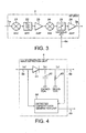
- Fig. 3 is a block diagram schematically showing the structure of the RF unit 2 in the automatic gain control system of the present embodiment.
- the RF unit 2 comprises a mixer (MIX) 21, a band-pass filter (BPF) 22, an amplifier (AMP) 23, a mixer (MIX) 24, a variable attenuator (variable ATT) 25, and an amplifier (AMP) 26.
- MIX mixer
- AMP amplifier
- AMP amplifier
- the MIX 21 upconverts the base-band signal 1a supplied by the control unit 1, the BPF 22 removes unnecessary waves other than the necessary frequency band, and the AMP 23 amplifies the signal to a power necessary for transmission.
- the variable ATT 25 varies the total gain of the RF unit 2 by using the offset signal (gain variation control signal) 6b supplied from the gain variation calculation circuit 5, which will be described hereinbelow.
- the AMP 26 amplifies an output signal from the variable ATT 25 to an amplitude having a desired magnitude.
- the amplified transmission wave 2a is supplied to the coupler 3, which is a post-processing component.
- This automatic gain control circuit controls the transmission output gain by feed-back (negative feed-back) of the envelope data 4a as transmission-power-value information of the transmission wave 2a supplied from the RF unit 2 and by control the variable ATT 25 in the RF unit 2.
- Fig. 4 is a circuit diagram showing the structure of the wave detector unit 4 in the automatic gain control system of the present embodiment.
- Figs. 5A to 5C are graphs showing output voltage waveforms which are detected by the wave detector unit 4.
- the wave detector unit 4 comprises a diode 41, a capacitor C 42, a resistor R 43, and a detected capacity data generator unit 44.
- the wave detector unit 4 outputs the envelope data 4a to the A/D converter 7 in the gain variation calculation unit 5 and also outputs the detected capacity information 4b to the comparing calculation circuit 6 in the gain variation calculation unit 5.
- the diode 41 inputs the coupling signal 3b supplied by the coupler 3, and half-wave rectifies a wave of the coupling signal 3b. Thereafter, the coupling signal 3b which is half-rectified charges/discharges the capacitor C 42 and the resistor R 43.
- the envelope data 4a is supplied to the A/D converter 7 in the gain variation calculation circuit 5 and the detected capacity data generator unit 44, which are post-processing components.
- the detected capacity data generator unit 44 outputs the detected capacity information 4b on the basis of the above-mentioned envelope data 4a and coupling signal 3b.
- the electrical power is increased by controlling the power as described above and a plurality of signals are also multiplexed for the sake of improving the availability of frequencies. Accordingly, this system handles the modulated wave having a marked variation in amplitude.
- Figs. 6A to 6C are diagrams showing the principle of deterioration of the average voltage due to a time constant of the wave detector unit of the present embodiment.
- V1 denotes an accurate detected voltage as a correct voltage
- V2 denotes a detected voltage of a modulated wave of an average voltage equal to V1.
- the gain variation calculation circuit 5 assumes that there is deterioration in the wave detector unit 4. More specifically, the comparator 8 compares the envelope data 4a obtained by multiplying the time constant data equivalent to the wave detector unit 4 with the reference data in which the base-band signal 1a generated by the control unit 1 is information. Thus, the variation caused by the detection is compensated for.
- Fig. 7 is a block diagram schematically showing the structure of the gain variation calculation circuit 5 in the automatic gain control system of the present embodiment.
- the gain variation calculation circuit 5 has the comparing calculation circuit 6 and the A/D converter 7 as mentioned above.
- the comparing calculation circuit 6 comprises the comparator 8, a time constant table 61, a multiplier 62, and a variable ATT control unit 63.
- the time constant table 61 is a table for storing the detected capacity information 4b (time constant CR in the wave detector unit 4) which is generated by the detected capacity data generator unit 44 in the wave detector unit 4.
- Envelope data 6b and discrete data 7a are inputted to the comparator 8.
- the envelope data 6b is obtained by multiplying the discrete data 1b inputted by the control unit 1 by a time constant CR, as the detected capacity information 4b, in the multiplier 62.
- the detected capacity information 4b is generated by the detected capacity data generator unit 44 whose data is stored in the time constant table 61.
- the A/D converter 7 converts the envelope data 4a outputted by the wave detector unit 4 into the discrete data 7a.
- This comparison result is outputted by the variable ATT control unit 63 of the post-processing component as processable data (offset data) 8f as will be described later on.
- the time constant multiplied by the multiplier 62 needs to be set in advance based on characteristics of the wave detector unit 4.
- the time constant is stored in the time constant table 61 as the detected capacity information 4b (for example, expressed in the form of a function expression). Two types of forming methods for the detected capacity information 4b are indicated as examples below.
- a detected capacity of the wave detector unit 4 is formulated and the obtained expression is stored in the detected capacity data generator unit 44.
- Fig. 8 is block diagram showing the structure of the comparator 8 in the gain variation calculation circuit 5 of the present embodiment.
- the comparator 8 comprises a first delay circuit 81, a second delay circuit 82, a first averaging circuit 83, a second averaging circuit 84, an adder 85, a multiplier 86, and a comparison value conversion table 87.
- the envelope data 6b which is obtained by multiplying the discrete data 1b by the time constant in the multiplier 62, is inputted to the first delay circuit 81.
- the discrete data 7a is inputted to the second delay circuit 82.
- the discrete data 7a is obtained by converting the envelope data 4a outputted by the wave detector unit 4 by the A/D converter 7.
- the first delay circuit 81 and the second delay circuit 82 assume that there is a delay differences due for the envelope data 6b and the discrete data 7a to propagation and calculation. More specifically, the first delay circuit 81 and the second delay circuit 82 form data 8a and 8b which are obtained by combining both comparison timings thereof.
- the first averaging circuit 83 and the second averaging circuit 84 average the inputted data 8a and 8b at an arbitrary interval, thereby obtaining average voltage values 8c and 8d.
- the adder 85 performs a differential process of a difference between the average voltage values 8c and 8d which are obtained by the average voltage values 83 and 84, thereby obtaining voltage difference data 8e.
- the multiplier 86 multiplies the voltage difference data 8e outputted from the adder 85 by the comparison value stored in the comparison value conversion table 87, thereby obtaining the processable data 8f in the variable ATT control unit 63, which is a post-processing component.
- Fig. 9 is a diagram showing a specific processing example of the first averaging circuit 83 and the second averaging circuit 84 of the present embodiment. As shown in Figs. 7 and 8, the discrete data 1 from the control unit 1 and the discrete data 7a of the envelope data 4a from the wave detector unit 4 are inputted to the first averaging circuit 83 and the second averaging circuit 84, respectively.
- an average voltage value V is calculated for an arbitrary interval T.
- the voltage difference data 8e is obtained by the differential process for obtained average voltage values V1 and V2. If the format of the average voltage data 8c and 8d is based on logarithm conversion, the average voltage data 8c and 8d must be compared under a condition using a logarithm format. On the other hand, if the format of the data is based on linear conversion, the average voltage data 8c and 8d must be compared under a condition using a linear format.
- the comparator 8 has the comparison value conversion table 87, and the obtained voltage difference data 8e is converted into an offset value.
- the processable data 8f, as offset data, is supplied to the variable ATT control unit 63 for controlling the amount of attenuation of the variable ATT 25 in the RF unit 2.
- the variable ATT control unit 63 converts the obtained offset data 8f into a voltage value, and supplies the voltage value to the variable ATT 25 as a control voltage, thereby varying the amount of attenuation.
- the voltage difference data 8e is +2V (lower than a transmission output level by 2dB)
- the voltage difference data 8e is converted into the offset data 8f having an offset value 0140.
- the control voltage to the variable ATT 25 in the RF unit 2 is set to +2.5V.
- the amount of attenuation of the variable ATT 25 is reduced by 2dB and the total gain of the RF unit 2 is corrected by +2dB.
- reference numeral V'1 denotes an average voltage of the base-band signal 1b generated by the control unit 1 over a certain time T1.
- the wave detector unit 4 detects this signal and the A/D converter 7 converts the detection signal into discrete data. Thereafter, an average voltage V'2 over a time T2 similar to T1 should be equivalent to V'1.
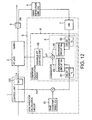
- Fig. 12 is a block diagram showing an operation model of the automatic gain control system in the present invention. Parameters shown in Fig. 12 are defined as follows.
- either one of ⁇ 1 and ⁇ 2 may be omitted in accordance with the processing time.
- variable ATT control unit 62 in Fig. 5 performs the following operation.
- ⁇ P >0 the variable ATT control unit 62 controls the variable ATT 25 in the RF unit 2, thereby increasing the gain.
- automatic gain control can be stably controlled in the case of handling a modulation wave having a marked variation in amplitude, such as CDMA.
- the automatic gain control system of the present invention for the base-band signal obtained by the control unit, deterioration in the wave detector unit is compensated for by multiplying the data which is equivalent to the time constant in the wave detector unit, thereby compensating for the difference caused by the time constant during detection. Accordingly, it is possible to compensate for the deterioration in the detection voltage generated when detecting the modulation wave having a marked variation in amplitude, such as CDMA, and also to obtain stable power outputted by the RF unit.
Landscapes
- Control Of Amplification And Gain Control (AREA)
- Transmitters (AREA)
Abstract
Description
Claims (12)
- An automatic gain control system wherein
a base-band signal serving as reference data of a transmission wave is multiplied by a time constant during detection, thereby compensating for an amount of deterioration in said transmission wave which is caused by said time constant during said detection. - An automatic gain control system comprising:a transmit-receive control unit for generating a base-band signal serving as reference data of a transmission wave;a radio frequency converter unit for converting a frequency of said base-band signal based on a gain variation control signal;a coupler unit for splitting said base-band signal of which frequency is converted;a wave detector unit for detecting one of the split base-band signal; anda gain variation calculation circuit for outputting to said radio frequency converter unit said gain variation control signal which is generated based on a detection result by said wave detector unit and discrete data of said base-band signal outputted by said transmit-receive control unit, and wherein:said wave detector unit outputs envelope data of the one of split base-band signal and detected capacity information having a time constant of said wave detector unit as said detection result, andsaid gain variation calculation circuit comprises;an A/D converter for converting said envelope data into discrete data, anda comparing calculation circuit for generating said gain variation control signal based on a result of comparing a value obtained by multiplying the discrete data of said base-band signal from said transmit-receive control unit by the time constant, as said detected capacity information, with the discrete data of said envelope data converted by said A/D converter.
- A system as claimed in Claim 2, wherein said transmit-receive control unit comprises:a serial-to-parallel converter for performing serial-to-parallel conversion of an input signal;an I/Q encoder for encoding the serial-to-parallel-converted signal by said serial-to-parallel converter to an I-channel signal and a Q-channel signal;a code for designating code information of said I-channel signal and said Q-channel signal encoded by said I/Q encoder;a modulator for modulating said I-channel signal and said Q-channel signal encoded by said I/Q encoder on the basis of the code information designated by said code;a power controller for controlling transmission powers of said I-channel signal and said Q-channel signal which are modulated by said modulator;at least two multipliers for controlling amplitude values of said I-channel signal and said Q-channel signal on the basis of said control of the transmission power by said power controller;a multiplexer for multiplexing said Ich signal and said Qch signal from said multiplier;a filter for limiting bands of said Ich signal and said Qch signal from said multiplexer;a quadrature modulator for synthesizing and quadrature-modulating said Ich signal and said Qch signal whose bands are limited by said filter;a frequency converter for converting a frequency of the signal quadrature-modulated by said quadrature modulator into a desired frequency; anda D/A converter for converting the signal which is converted into the desired frequency by said frequency converter into an analog signal, andsaid transmit-receive control unit outputs said signal quadrature-modulated by said quadrature modulator to said comparing calculation circuit as the discrete data of said base-band signal, and further outputs said analog signal converted by said D/A converter to said radio frequency converter unit as said base-band signal.
- A system as claimed in Claim 2, wherein said radio frequency converter unit comprises:a first mixer for upconverting said base-band signal from said transmit-receive control unit;a band-pass filter for removing unnecessary waves other than a necessary frequency band from an output from said first mixer;a first amplifier for amplifying an output from said band-pass filter to a necessary power;a second mixer for upconverting the output amplified by said first amplifier;a variable attenuator for varying a gain of an output from said second mixer based on said gain variation control signal; anda second amplifier for amplifying an output from said variable attenuator to an output having a desired magnitude.
- A system as claimed in Claim 3, wherein said radio frequency converter unit comprises:a first mixer for upconverting said base-band signal from said transmit-receive control unit;a band-pass filter for removing unnecessary waves other than a necessary frequency band from an output from said first mixer;a first amplifier for amplifying an output from said band-pass filter to a necessary power;a second mixer for upconverting the output amplified by said first amplifier;a variable attenuator for varying a gain of an output from said second mixer based on said gain variation control signal; anda second amplifier for amplifying an output from said variable attenuator to an output having a desired magnitude.
- A system as claimed in Claim 2, wherein:
said coupler unit directly outputs said base-band signal, without changing said signal, whose gain is controlled by said radio frequency converter unit based on said gain variation control signal as a transmission wave, and supplies a signal obtained by splitting 1/N of said gain variation control signal, where N is an integer equal to 1 or more, to said wave detector unit. - A system as claimed in Claim 3, wherein:
said coupler unit directly outputs said base-band signal, without changing said signal, whose gain is controlled by said radio frequency converter unit based on said gain variation control signal as a transmission wave, and supplies a signal obtained splitting 1/N of said gain variation control signal, where N is an integer equal to 1, to said wave detector unit. - A system as claimed in Claim 4, wherein:
said coupler unit directly outputs said base-band signal, without changing said signal, whose gain is controlled by said radio frequency converter unit based on said gain variation control signal as a transmission wave, and supplies a signal obtained by splitting 1/N of said gain variation control signal, where N is an integer equal to 1 or more to said wave detector unit. - A system as claimed in Claim 5, wherein:
said coupler unit directly outputs said base-band signal, without changing said signal, whose gain is controlled by said radio frequency converter unit based on said gain variation control signal as a transmission wave, and supplies a signal obtained by splitting 1/N of said gain variation control signal, where N is an integer equal to 1 or more to said wave detector unit. - A system as claimed in Claim 2, wherein said comparing calculation circuit comprises:a time constant table in which said time constant, as said detected capacity information from said wave detector unit, is stored;a multiplier circuit for multiplying the discrete data of said base-band signal from said transmit-receive control unit by said time constant stored in said time constant table and for outputting discrete data;a comparator for comparing the discrete data from said multiplier circuit with the discrete data from said A/D converter; anda variable attenuator control unit for generating said gain variation control signal for controlling conversion by said variable attenuator based on a comparison result by said comparator.
- A system as claimed in Claims 3 through 9, wherein said comparing calculation circuit comprises:a time constant table in which said time constant, as said detected capacity information from said wave detector unit, is stored;a multiplier circuit for multiplying the discrete data of said base-band signal from said transmit-receive control unit by said time constant stored in said time constant table and for outputting the discrete data;a comparator for comparing the discrete data from said multiplier circuit with the discrete data from said A/D converter; anda variable attenuator control unit for generating said gain variation control signal for controlling conversion by said variable attenuator based on a comparison result by said comparator.
- A system as claimed in Claim 10, wherein said comparator comprises:a first delay circuit for delaying the discrete data from said multiplier circuit by an arbitrary time;a second delay circuit for delaying the discrete data from said A/D converter by an arbitrary time;a first averaging circuit for averaging an output from said first delay circuit over a predetermined time;a second averaging circuit for averaging an output from said second delay circuit over said predetermined time;an adder for adding an output from said first averaging circuit and an output from said second averaging circuit and for outputting an average voltage value;a comparison value conversion table in which a comparison value for said average voltage value outputted from said adder is stored; anda multiplier for multiplying said average voltage value by said comparison value stored in said comparison value conversion table.
Applications Claiming Priority (2)
| Application Number | Priority Date | Filing Date | Title |
|---|---|---|---|
| JP2000088521 | 2000-03-24 | ||
| JP2000088521A JP3544506B2 (en) | 2000-03-24 | 2000-03-24 | Automatic gain control device |
Publications (2)
| Publication Number | Publication Date |
|---|---|
| EP1137174A2 true EP1137174A2 (en) | 2001-09-26 |
| EP1137174A3 EP1137174A3 (en) | 2004-05-12 |
Family
ID=18604393
Family Applications (1)
| Application Number | Title | Priority Date | Filing Date |
|---|---|---|---|
| EP01107267A Withdrawn EP1137174A3 (en) | 2000-03-24 | 2001-03-23 | Automatic gain control system |
Country Status (4)
| Country | Link |
|---|---|
| US (1) | US6795694B2 (en) |
| EP (1) | EP1137174A3 (en) |
| JP (1) | JP3544506B2 (en) |
| BR (1) | BR0101572A (en) |
Families Citing this family (26)
| Publication number | Priority date | Publication date | Assignee | Title |
|---|---|---|---|---|
| JP3501766B2 (en) | 2001-03-26 | 2004-03-02 | 埼玉日本電気株式会社 | Reference signal clip control method |
| EP1271768A1 (en) * | 2001-06-19 | 2003-01-02 | u- blox-ag | Analog base band unit for a RF receiver |
| JP3908508B2 (en) * | 2001-11-13 | 2007-04-25 | 新潟精密株式会社 | Automatic gain control circuit |
| EP1315292B1 (en) * | 2001-11-21 | 2006-09-13 | Sony Deutschland GmbH | Digital controlled AGC |
| US7277678B2 (en) * | 2002-10-28 | 2007-10-02 | Skyworks Solutions, Inc. | Fast closed-loop power control for non-constant envelope modulation |
| US7133651B2 (en) * | 2002-11-04 | 2006-11-07 | Lg Electronics Inc. | Transmission apparatus for mobile communication terminal |
| US7386074B1 (en) | 2003-10-06 | 2008-06-10 | Redpine Signals, Inc. | Digital automatic gain control method and apparatus |
| FR2871629A1 (en) * | 2004-06-09 | 2005-12-16 | Thomson Licensing Sa | FREQUENCY CONVERTING DEVICE, METHOD OF CALIBRATING THE DEVICE, AND SYSTEM FOR TRANSMITTING / RECEIVING ELECTROMAGNETIC SIGNALS HAVING SUCH A DEVICE |
| US7596355B2 (en) * | 2004-11-29 | 2009-09-29 | Intel Corporation | System and method capable of closed loop MIMO calibration |
| KR100690788B1 (en) * | 2005-02-26 | 2007-03-09 | 엘지전자 주식회사 | Power compensation method of mobile communication terminal |
| US8116485B2 (en) * | 2005-05-16 | 2012-02-14 | Qnx Software Systems Co | Adaptive gain control system |
| WO2007004518A1 (en) * | 2005-06-30 | 2007-01-11 | Matsushita Electric Industrial Co., Ltd. | Transmission circuit and communication device |
| US7729671B2 (en) * | 2006-12-06 | 2010-06-01 | Broadcom Corporation | Method and system for enhancing efficiency by modulating power amplifier gain |
| US7941109B2 (en) | 2007-01-12 | 2011-05-10 | Panasonic Corporation | Polar modulation transmission apparatus and transmission power control method |
| US7656227B1 (en) | 2008-02-26 | 2010-02-02 | Pmc-Sierra, Inc. | Techniques to control amplifier gain over process, voltage, and/or temperature (PVT) variations |
| US8099139B1 (en) | 2008-03-06 | 2012-01-17 | Marvell International Ltd. | Power control using fast signal envelope detection |
| US8781536B1 (en) | 2008-03-06 | 2014-07-15 | Marvell International Ltd | Power control using fast signal correlation |
| JP4336903B1 (en) | 2008-03-27 | 2009-09-30 | 日本電気株式会社 | Transmission circuit and wireless communication device |
| JP2010187274A (en) * | 2009-02-13 | 2010-08-26 | Nec Network & Sensor Systems Ltd | Level adjustment circuit of high frequency amplifier, and level control method of high frequency amplifier |
| US8238845B2 (en) * | 2009-09-22 | 2012-08-07 | Broadcom Europe Limited | Radio frequency circuit |
| US8737941B2 (en) * | 2010-03-30 | 2014-05-27 | Skyworks Solutions, Inc. | Gain control systems and methods for controlling an adjustable power level |
| WO2014081738A1 (en) | 2012-11-21 | 2014-05-30 | Marvell World Trade Ltd. | Method for fast automatic power control of wireless transmitters |
| US9432110B2 (en) * | 2014-05-07 | 2016-08-30 | The Boeing Company | System and method for code multiplexing |
| JP6538585B2 (en) * | 2016-02-17 | 2019-07-03 | 株式会社東芝 | Modulated signal generating device and wireless device |
| DE102017209209A1 (en) * | 2017-05-31 | 2018-12-06 | Laird Dabendorf Gmbh | Signal coupling device and method for operating a signal coupling device |
| US10432447B2 (en) | 2017-11-10 | 2019-10-01 | The Boeing Company | System and method for amplitude pre-distortion optimization for GPS signal constant envelope transmission |
Family Cites Families (12)
| Publication number | Priority date | Publication date | Assignee | Title |
|---|---|---|---|---|
| JPS5875308A (en) * | 1981-10-29 | 1983-05-07 | Matsushita Electric Ind Co Ltd | demodulator |
| JPH07118617B2 (en) * | 1990-07-19 | 1995-12-18 | 沖電気工業株式会社 | Power amplifier and transmitter |
| JP2826003B2 (en) * | 1991-11-29 | 1998-11-18 | 松下電器産業株式会社 | Transmission output control circuit |
| JPH0730444A (en) * | 1993-07-08 | 1995-01-31 | Fujitsu Ltd | Transmitter |
| JPH07336243A (en) | 1994-06-10 | 1995-12-22 | Matsushita Electric Ind Co Ltd | Transmission output control device |
| JP2967699B2 (en) * | 1995-03-06 | 1999-10-25 | 日本電気株式会社 | Transmission device |
| US5852770A (en) * | 1995-09-19 | 1998-12-22 | Sanyo Electric Co., Ltd. | Transmission power control device for a portable terminal |
| US5712593A (en) * | 1996-02-05 | 1998-01-27 | Motorola, Inc. | Linear power amplifier with distortion detection |
| CA2172873C (en) * | 1996-03-28 | 2002-03-12 | Kim Byron Roberts | Method of determining optical amplifier failures |
| JPH10145161A (en) * | 1996-11-13 | 1998-05-29 | Nec Corp | Pre-distortion automatic adjustment circuit |
| JPH11220346A (en) * | 1998-02-02 | 1999-08-10 | Fujitsu Ltd | Automatic gain control circuit |
| US6069530A (en) * | 1998-09-16 | 2000-05-30 | Motorola, Inc. | Apparatus and method for linear power amplification |
-
2000
- 2000-03-24 JP JP2000088521A patent/JP3544506B2/en not_active Expired - Fee Related
-
2001
- 2001-03-23 BR BR0101572-9A patent/BR0101572A/en not_active IP Right Cessation
- 2001-03-23 EP EP01107267A patent/EP1137174A3/en not_active Withdrawn
- 2001-03-26 US US09/816,353 patent/US6795694B2/en not_active Expired - Fee Related
Also Published As
| Publication number | Publication date |
|---|---|
| JP3544506B2 (en) | 2004-07-21 |
| EP1137174A3 (en) | 2004-05-12 |
| JP2001274646A (en) | 2001-10-05 |
| US6795694B2 (en) | 2004-09-21 |
| US20010027090A1 (en) | 2001-10-04 |
| BR0101572A (en) | 2001-11-13 |
Similar Documents
| Publication | Publication Date | Title |
|---|---|---|
| US6795694B2 (en) | Automatic gain control system | |
| KR100367433B1 (en) | Transmitter | |
| US7023897B2 (en) | Transmission circuit | |
| EP1687893B1 (en) | Predistortion control device and method, assembly including a predistortion control device | |
| EP1285508B1 (en) | Method for determining the gains of different carriers, radio transmission unit and module for such unit | |
| US6868279B2 (en) | Power characteristic of a radio transmitter | |
| US7103029B1 (en) | Transmitter gain stabilizing apparatus | |
| US7489907B2 (en) | Transmitter for suppressing a variation in input level of a multicarrier signal | |
| KR100740177B1 (en) | Method and apparatus for compensating mismatch of transmitter using nonlinear envelope detector | |
| US20050101254A1 (en) | Distortion compensating amplifier | |
| KR20040066003A (en) | An uncorrelated adaptive predistorter | |
| CN102037699A (en) | Distortion compensation circuit and distortion compensation method | |
| US5293407A (en) | Digital modulator with digital power control circuit | |
| US8433268B2 (en) | Apparatus and method for controlling gain of polar transmitter | |
| KR100303371B1 (en) | Radio transmitting apparatus and gain control method for the same | |
| JPH10322270A (en) | Transmission power control device | |
| JP4318253B2 (en) | Transmitter | |
| US7551905B2 (en) | Distortion compensation apparatus | |
| US9853608B2 (en) | Temperature compensation technique for envelope tracking system | |
| JPH08204605A (en) | Radio and how to use the radio | |
| EP1569350B1 (en) | Power limit device and digital radio transmitter using the same | |
| EP1185016A1 (en) | Multiplex communication system and method of signal processing | |
| KR100737747B1 (en) | Method and apparatus for compensating mismatch of transmitter | |
| JP2000244341A (en) | Saturation prevention circuit in Cartesian feedback circuit | |
| JP3891270B2 (en) | Automatic gain controller |
Legal Events
| Date | Code | Title | Description |
|---|---|---|---|
| PUAI | Public reference made under article 153(3) epc to a published international application that has entered the european phase |
Free format text: ORIGINAL CODE: 0009012 |
|
| AK | Designated contracting states |
Kind code of ref document: A2 Designated state(s): AT BE CH CY DE DK ES FI FR GB GR IE IT LI LU MC NL PT SE TR |
|
| AX | Request for extension of the european patent |
Free format text: AL;LT;LV;MK;RO;SI |
|
| PUAL | Search report despatched |
Free format text: ORIGINAL CODE: 0009013 |
|
| AK | Designated contracting states |
Kind code of ref document: A3 Designated state(s): AT BE CH CY DE DK ES FI FR GB GR IE IT LI LU MC NL PT SE TR |
|
| AX | Request for extension of the european patent |
Extension state: AL LT LV MK RO SI |
|
| 17P | Request for examination filed |
Effective date: 20040405 |
|
| 17Q | First examination report despatched |
Effective date: 20040710 |
|
| AKX | Designation fees paid |
Designated state(s): DE GB |
|
| STAA | Information on the status of an ep patent application or granted ep patent |
Free format text: STATUS: THE APPLICATION HAS BEEN WITHDRAWN |
|
| 18W | Application withdrawn |
Effective date: 20050930 |