EP1137159A2 - Integrated controller for synchronous rectifiers - Google Patents
Integrated controller for synchronous rectifiers Download PDFInfo
- Publication number
- EP1137159A2 EP1137159A2 EP01106962A EP01106962A EP1137159A2 EP 1137159 A2 EP1137159 A2 EP 1137159A2 EP 01106962 A EP01106962 A EP 01106962A EP 01106962 A EP01106962 A EP 01106962A EP 1137159 A2 EP1137159 A2 EP 1137159A2
- Authority
- EP
- European Patent Office
- Prior art keywords
- transistors
- power converter
- synchronous rectifier
- switching power
- voltage
- Prior art date
- Legal status (The legal status is an assumption and is not a legal conclusion. Google has not performed a legal analysis and makes no representation as to the accuracy of the status listed.)
- Withdrawn
Links
Images



Classifications
-
- H—ELECTRICITY
- H02—GENERATION; CONVERSION OR DISTRIBUTION OF ELECTRIC POWER
- H02M—APPARATUS FOR CONVERSION BETWEEN AC AND AC, BETWEEN AC AND DC, OR BETWEEN DC AND DC, AND FOR USE WITH MAINS OR SIMILAR POWER SUPPLY SYSTEMS; CONVERSION OF DC OR AC INPUT POWER INTO SURGE OUTPUT POWER; CONTROL OR REGULATION THEREOF
- H02M1/00—Details of apparatus for conversion
- H02M1/38—Means for preventing simultaneous conduction of switches
-
- H—ELECTRICITY
- H02—GENERATION; CONVERSION OR DISTRIBUTION OF ELECTRIC POWER
- H02M—APPARATUS FOR CONVERSION BETWEEN AC AND AC, BETWEEN AC AND DC, OR BETWEEN DC AND DC, AND FOR USE WITH MAINS OR SIMILAR POWER SUPPLY SYSTEMS; CONVERSION OF DC OR AC INPUT POWER INTO SURGE OUTPUT POWER; CONTROL OR REGULATION THEREOF
- H02M3/00—Conversion of DC power input into DC power output
- H02M3/22—Conversion of DC power input into DC power output with intermediate conversion into AC
- H02M3/24—Conversion of DC power input into DC power output with intermediate conversion into AC by static converters
- H02M3/28—Conversion of DC power input into DC power output with intermediate conversion into AC by static converters using discharge tubes with control electrode or semiconductor devices with control electrode to produce the intermediate AC
- H02M3/325—Conversion of DC power input into DC power output with intermediate conversion into AC by static converters using discharge tubes with control electrode or semiconductor devices with control electrode to produce the intermediate AC using devices of a triode or a transistor type requiring continuous application of a control signal
- H02M3/335—Conversion of DC power input into DC power output with intermediate conversion into AC by static converters using discharge tubes with control electrode or semiconductor devices with control electrode to produce the intermediate AC using devices of a triode or a transistor type requiring continuous application of a control signal using semiconductor devices only
- H02M3/33569—Conversion of DC power input into DC power output with intermediate conversion into AC by static converters using discharge tubes with control electrode or semiconductor devices with control electrode to produce the intermediate AC using devices of a triode or a transistor type requiring continuous application of a control signal using semiconductor devices only having several active switching elements
- H02M3/33576—Conversion of DC power input into DC power output with intermediate conversion into AC by static converters using discharge tubes with control electrode or semiconductor devices with control electrode to produce the intermediate AC using devices of a triode or a transistor type requiring continuous application of a control signal using semiconductor devices only having several active switching elements having at least one active switching element at the secondary side of an isolation transformer
- H02M3/33592—Conversion of DC power input into DC power output with intermediate conversion into AC by static converters using discharge tubes with control electrode or semiconductor devices with control electrode to produce the intermediate AC using devices of a triode or a transistor type requiring continuous application of a control signal using semiconductor devices only having several active switching elements having at least one active switching element at the secondary side of an isolation transformer having a synchronous rectifier circuit or a synchronous freewheeling circuit at the secondary side of an isolation transformer
-
- Y—GENERAL TAGGING OF NEW TECHNOLOGICAL DEVELOPMENTS; GENERAL TAGGING OF CROSS-SECTIONAL TECHNOLOGIES SPANNING OVER SEVERAL SECTIONS OF THE IPC; TECHNICAL SUBJECTS COVERED BY FORMER USPC CROSS-REFERENCE ART COLLECTIONS [XRACs] AND DIGESTS
- Y02—TECHNOLOGIES OR APPLICATIONS FOR MITIGATION OR ADAPTATION AGAINST CLIMATE CHANGE
- Y02B—CLIMATE CHANGE MITIGATION TECHNOLOGIES RELATED TO BUILDINGS, e.g. HOUSING, HOUSE APPLIANCES OR RELATED END-USER APPLICATIONS
- Y02B70/00—Technologies for an efficient end-user side electric power management and consumption
- Y02B70/10—Technologies improving the efficiency by using switched-mode power supplies [SMPS], i.e. efficient power electronics conversion e.g. power factor correction or reduction of losses in power supplies or efficient standby modes
Definitions
- the present invention relates to an integrated gate drive controller for synchronous rectifiers. More specifically, the present invention relates to an integrated gate drive controller for synchronous rectifiers that minimizes secondary side stray inductance effects by controlling overlap of the gate drive signals.
- the power converter disclosed in U.S. Pat. No. 6,026,005 includes a modified PLL with an adjustable delay block in the feedback path that forces the V CO output signal to lead the input signal.
- One drawback that is not addressed by the power converter of U.S. Pat. No. 6,026,005 is the effect of stray inductances in the secondary side. These stray inductances are disadvantagous in that they maintain a current flow even if the MOSFETs with which they are associated have zero tun-on/off times. This results in MOSFET body diode conduction and unnecessary losses until the current dissipates.
- the present invention overcomes the deficiencies of the prior art, such as those noted above, by providing synchronous rectifier circuit driver that controls dead time/overlap of the rectifier transistor gates.
- a switching power converter includes a switching transformer having a primary winding and a secondary winding.
- the secondary winding has first and second voltage nodes across which a winding voltage having a phase and a variable duty cycle is impressed.
- a first synchronous rectifier transistor is coupled from the first voltage node to a common node, and a second synchronous rectifier transistor is coupled from the second voltage node to the common node.
- a driver circuit receives the winding voltage and produces first and second drive signals to the first and second synchronous rectifier transistors, respectively.
- the driver circuit is operable to maintain both transistors on at the same time for a short period, such that induction currents are allowed to dissipate through the transistors rather than the transistor body diode. Accordingly, conduction losses are reduced.
- dead time/overlap control is provided by a pair of NOR latches having inputs and outputs interconnected.
- the output gate drives will cross at approximately 50% of Vdd.
- Addition of resistors and capacitors will reduce the crossover point from 1 ⁇ 2 Vdd and result in a dead time (no overlap) between the turn-off of one synchronous rectifier device and the turn-on of the other.
- both overlap and dead time of gate drives are used in the same converter circuit at different switching cycles.
- overlap is used at the transition from the reset cycle to the power transfer cycle.
- a slight amount of dead time is used to prevent cross conduction. This is required due to the latency of the transformer turn off (due to stray magnetizing inductance, capacitance and/or stray inductance of the transformer).
- the amount of dead time is primarily dictated by circuit parasitics.
- Fig. 1 is a schematic representation of the secondary side of a power converter showing stray inductances.
- Fig. 2 is a graph illustrating MOSFET body diode conduction with dead time in gate drives, resulting in high peak body diode currents as shown by the left side graphs, compared to the effects of overlapped gate drives resulting in reduced body diode conduction and reduced losses as shown by the right side graphs.
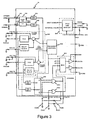
- Fig. 3 is a diagram of the integrated synchronous rectifier controller of the present invention.
- Fig. 4 is a typical connection diagram of the synchronous rectifier controller of the present invention with a single ended forward converter circuit.
- a schematic diagram shows a power converter 2 employing the synchronous rectifier controller of the present invention.
- the converter circuit 2 includes a pair of MOSFET transistors, Q1 and Q2 , arranged to switch the voltage at the secondary winding of a transformer, XFRMR .
- MOSFET transistors Q1 and Q2
- XFRMR transformer
- IGBTs with integral diodes could be used.
- the switching of the MOSFETs Q1 and Q2 of converter circuit 2 is controlled by synchronous rectifier control circuit 4 which has IN , GND , Q1 G , and Q2 G terminals and is preferably provided in integrated form.
- Gate driver 4 has an IN terminal connected to the XFRMR winding. Terminals Q1 G and Q2 G provide drive signals to the gates of Q1 and Q2, respectively.
- Body diodes of transistors Q1 and Q2 are represented by diodes BD1 and BD2 , respectively.
- L(Stray) 1 and L(Stray) 2 represent stray inductances. Secondary branch currents through transistors Q1 and Q2 are indicated by the arrows labeled I1 and I2 , respectively.
- Figs. 2A and 2B a pair of graphs is shown illustrating the body diode current in the power converter of Fig. 1. Stray inductances cause secondary branch currents to ramp up or down slowly during transformer transitions.
- Fig. 2A shows MOSFET body diode conduction with dead time t D in gate drives results in high peak body diode currents. With dead time between the gate drives, when each device turns off, the stray inductance will force the current through the body diode. Current will ramp down in one branch while ramping up in the other.
- the overlapped gate drives show reduced conduction and hence, reduced losses.
- the currents are allowed to dissipate through the MOSFET rather than the body diode, thereby reducing losses.
- Rectifier 10 includes a transformer input X1 for transistor Q1 , and a transformer input X2 for transistor Q2 .
- a +5 Vdc supply voltage is connected to pin VDD for powering the internal logic of the controller.
- VOUTA and VOUTB supply gate signals to transistors Q1 and Q2 , respectively.
- DTIN1 and DTOUT1 are used to set the dead time/overlap for the gate output VOUTA to Q1 .
- DTIN2 and DTOUT2 are used to set the dead time/overlap for the gate output VOUTB to Q2 .
- controller 10 includes a pair of Schmitt trigger circuits 101 and 102 , a double pulse suppression circuit 104 , a pair of edge detector circuits 220 and 222 , a phase-locked loop circuit 300 , and an output regeneration circuit 400 .
- the gate drive circuit 10 In order to accommodate transitions between operating modes (i.e., the normal mode, off mode, and cross coupled mode), the gate drive circuit 10 also employs an undervoltage lock-out circuit 500 , a transient control circuit 750 , and multiplexing circuit (or output select circuit) 800 .
- Dead time/overlap control is provided by NOR latches 1000 and 1002 with DTIN1/DTOUT1 and DTIN2/DTOUT2 inputs and outputs as shown in Fig 3.
- FIG. 4 a typical connection diagram for the gate driver of the present invention is shown.
- Topologies using extended gate drives will need to employ a slight dead time at both transitions to ensure no cross conduction occurs.
Landscapes
- Engineering & Computer Science (AREA)
- Power Engineering (AREA)
- Rectifiers (AREA)
- Dc-Dc Converters (AREA)
- Power Conversion In General (AREA)
Abstract
Description
voltage having a phase and a variable duty cycle is impressed. A first synchronous rectifier transistor is coupled from the first voltage node to a common node, and a second synchronous rectifier transistor is coupled from the second voltage node to the common node. A driver circuit receives the winding voltage and produces first and second drive signals to the first and second synchronous rectifier transistors, respectively. The driver circuit is operable to maintain both transistors on at the same time for a short period, such that induction currents are allowed to dissipate through the transistors rather than the transistor body diode. Accordingly, conduction losses are reduced.
Claims (6)
- A switching power converter, comprising:a switching transformer having a primary winding and a secondary winding, the secondary winding having first and second voltage nodes across which a winding
voltage having a phase and a variable duty cycle is impressed;a first synchronous rectifier transistor switch coupled from the first voltage node to a common node;a second synchronous rectifier transistor coupled from the second voltage node to the common node; anda gate driver circuit operable to produce first and second drive signals to the respective gates of the first and second synchronous rectifier transistors based upon the winding voltage, so as to maintain both transistors on at the same time for a short period such that currents through the transistor switches dissipate through the transistors rather than through body diodes of the transistors to thereby reduce conduction losses. - The switching power converter of claim 1, wherein said first and second synchronous rectifier transistors comprise power MOSFETs.
- The switching power converter of claim 1, wherein said first and second synchronous rectifier transistors comprise IGBTs.
- The switching power converter of claim 1, wherein the amount of overlap during which both transistors are simultaneously on is controllable by external components connected to pins of said gate driver circuit.
- The switching power converter of claim 4, wherein said external components comprise resistors and capacitors.
- The switching power converter of claim 4, wherein said external components are selected so as to result in both overlap and dead time of gate drive signals from said gate driver circuit at different switching cycles
Applications Claiming Priority (2)
| Application Number | Priority Date | Filing Date | Title |
|---|---|---|---|
| US19091500P | 2000-03-21 | 2000-03-21 | |
| US190915 | 2000-03-21 |
Publications (2)
| Publication Number | Publication Date |
|---|---|
| EP1137159A2 true EP1137159A2 (en) | 2001-09-26 |
| EP1137159A3 EP1137159A3 (en) | 2002-08-21 |
Family
ID=22703316
Family Applications (1)
| Application Number | Title | Priority Date | Filing Date |
|---|---|---|---|
| EP01106962A Withdrawn EP1137159A3 (en) | 2000-03-21 | 2001-03-20 | Integrated controller for synchronous rectifiers |
Country Status (3)
| Country | Link |
|---|---|
| US (1) | US6577518B2 (en) |
| EP (1) | EP1137159A3 (en) |
| JP (1) | JP3426586B2 (en) |
Cited By (1)
| Publication number | Priority date | Publication date | Assignee | Title |
|---|---|---|---|---|
| DE10323445B4 (en) * | 2003-05-23 | 2015-04-02 | Seuffer gmbH & Co. KG | Direct commutation between power components |
Families Citing this family (7)
| Publication number | Priority date | Publication date | Assignee | Title |
|---|---|---|---|---|
| JP4274353B2 (en) * | 2003-03-13 | 2009-06-03 | 本田技研工業株式会社 | Bidirectional DC-DC converter |
| US8134851B2 (en) * | 2003-11-04 | 2012-03-13 | International Rectifier Corporation | Secondary side synchronous rectifier for resonant converter |
| US7408796B2 (en) * | 2003-11-04 | 2008-08-05 | International Rectifier Corporation | Integrated synchronous rectifier package |
| US6961256B2 (en) * | 2004-02-13 | 2005-11-01 | Niko Semiconductor Co., Ltd. | Synchronous rectifier with dead time adjusting function |
| US7492138B2 (en) * | 2004-04-06 | 2009-02-17 | International Rectifier Corporation | Synchronous rectifier circuits and method for utilizing common source inductance of the synchronous FET |
| JP5532794B2 (en) * | 2009-09-28 | 2014-06-25 | 富士電機株式会社 | Synchronous rectification control device, control method, and isolated switching power supply |
| CN118232711B (en) * | 2023-12-29 | 2025-10-17 | 比亚迪股份有限公司 | Power module, motor controller, power assembly and vehicle |
Family Cites Families (11)
| Publication number | Priority date | Publication date | Assignee | Title |
|---|---|---|---|---|
| US4519024A (en) * | 1983-09-02 | 1985-05-21 | At&T Bell Laboratories | Two-terminal transistor rectifier circuit arrangement |
| US4922404A (en) * | 1989-03-15 | 1990-05-01 | General Electric Company | Method and apparatus for gating of synchronous rectifier |
| US5179512A (en) * | 1991-09-18 | 1993-01-12 | General Electric Company | Gate drive for synchronous rectifiers in resonant converters |
| GB2313495B (en) | 1996-05-20 | 2000-11-01 | Int Rectifier Corp | Synchronizing/driving circuit for a forward synchronous rectifier |
| US5818704A (en) * | 1997-04-17 | 1998-10-06 | International Rectifier Corporation | Synchronizing/driving circuit for a forward synchronous rectifier |
| US5870299A (en) * | 1997-05-28 | 1999-02-09 | Lucent Technologies Inc. | Method and apparatus for damping ringing in self-driven synchronous rectifiers |
| US6026005A (en) | 1997-06-11 | 2000-02-15 | International Rectifier Corp. | Single ended forward converter with synchronous rectification and delay circuit in phase-locked loop |
| JP3280615B2 (en) | 1998-02-18 | 2002-05-13 | ティーディーケイ株式会社 | Switching power supply |
| JPH11308862A (en) | 1998-04-24 | 1999-11-05 | Nec Fukushima Ltd | Switching power supply circuit |
| US6239994B1 (en) * | 1998-05-26 | 2001-05-29 | International Rectifier Corp | Secondary side switching regulator having a phase lock loop control circuit |
| US5940287A (en) | 1998-07-14 | 1999-08-17 | Lucent Technologies Inc. | Controller for a synchronous rectifier and power converter employing the same |
-
2001
- 2001-03-20 EP EP01106962A patent/EP1137159A3/en not_active Withdrawn
- 2001-03-20 US US09/811,697 patent/US6577518B2/en not_active Expired - Lifetime
- 2001-03-21 JP JP2001080618A patent/JP3426586B2/en not_active Expired - Fee Related
Cited By (1)
| Publication number | Priority date | Publication date | Assignee | Title |
|---|---|---|---|---|
| DE10323445B4 (en) * | 2003-05-23 | 2015-04-02 | Seuffer gmbH & Co. KG | Direct commutation between power components |
Also Published As
| Publication number | Publication date |
|---|---|
| JP2001352761A (en) | 2001-12-21 |
| US6577518B2 (en) | 2003-06-10 |
| US20010038546A1 (en) | 2001-11-08 |
| EP1137159A3 (en) | 2002-08-21 |
| JP3426586B2 (en) | 2003-07-14 |
Similar Documents
| Publication | Publication Date | Title |
|---|---|---|
| US9966837B1 (en) | Power converter with circuits for providing gate driving | |
| JP4436329B2 (en) | Isolated gate driver circuit for power switching devices | |
| JP4188335B2 (en) | Synchronous rectifier circuit and method for utilizing the common source inductance of this synchronous FET | |
| US6081432A (en) | Active reset forward converter employing synchronous rectifiers | |
| US7345896B2 (en) | Secondary side power supply controller and method therefor | |
| US6061255A (en) | Drive circuit for synchronous rectifiers in isolated forward converter | |
| US20020125920A1 (en) | Half-bridge gate driver circuit | |
| EP3509203B1 (en) | Converter with zvs | |
| US5635867A (en) | High performance drive structure for MOSFET power switches | |
| US6909620B2 (en) | Inverter configurations with shoot-through immunity | |
| JP7072709B1 (en) | Bipolar pulse voltage gate driver | |
| US7570087B2 (en) | Switching drive circuit for soft switching | |
| US7265525B2 (en) | Self-driven scheme for synchronous rectifier having no body diode | |
| JPH0549251A (en) | Method for minimizing switching loss in power switching device | |
| US7248093B2 (en) | Bipolar bootstrap top switch gate drive for half-bridge semiconductor power topologies | |
| CN115411711A (en) | Normally-off power switch with integrated fail-safe pull-down circuit and controllable turn-off time | |
| US6577518B2 (en) | Integrated controller for synchronous rectifiers | |
| US6023158A (en) | Switch drive controller, method of operation thereof and power converter employing the same | |
| Deneke et al. | 31.10 A fully integrated 500V, 6.25 MHz GaN-IC for totem-pole PFC off-line power conversion | |
| US7508175B2 (en) | System and method for reducing body diode conduction | |
| Matrisciano et al. | Universal isolated gate driving platform for 650 v gan hemts half-bridge with dead-time control and integrated bias supply | |
| KR102887825B1 (en) | A half bridge power conversion circuit | |
| US20250350278A1 (en) | System and method for driving a hybrid switch | |
| Dwane et al. | A resonant high side gate driver for low voltage applications | |
| KR100740355B1 (en) | Isolated Gate Driver Circuit for Power Switching Devices |
Legal Events
| Date | Code | Title | Description |
|---|---|---|---|
| PUAI | Public reference made under article 153(3) epc to a published international application that has entered the european phase |
Free format text: ORIGINAL CODE: 0009012 |
|
| AK | Designated contracting states |
Kind code of ref document: A2 Designated state(s): AT BE CH CY DE DK ES FI FR GB GR IE IT LI LU MC NL PT SE TR |
|
| AX | Request for extension of the european patent |
Free format text: AL;LT;LV;MK;RO;SI |
|
| PUAL | Search report despatched |
Free format text: ORIGINAL CODE: 0009013 |
|
| AK | Designated contracting states |
Kind code of ref document: A3 Designated state(s): AT BE CH CY DE DK ES FI FR GB GR IE IT LI LU MC NL PT SE TR |
|
| AX | Request for extension of the european patent |
Free format text: AL;LT;LV;MK;RO;SI |
|
| 17P | Request for examination filed |
Effective date: 20030221 |
|
| AKX | Designation fees paid |
Designated state(s): AT BE CH CY DE DK ES FI FR GB GR IE IT LI LU MC NL PT SE TR |
|
| STAA | Information on the status of an ep patent application or granted ep patent |
Free format text: STATUS: THE APPLICATION HAS BEEN WITHDRAWN |
|
| 18W | Application withdrawn |
Effective date: 20030604 |