EP1137133A1 - Quantum cascade laser having distributed feedback for single-mode cw operation - Google Patents
Quantum cascade laser having distributed feedback for single-mode cw operation Download PDFInfo
- Publication number
- EP1137133A1 EP1137133A1 EP00307623A EP00307623A EP1137133A1 EP 1137133 A1 EP1137133 A1 EP 1137133A1 EP 00307623 A EP00307623 A EP 00307623A EP 00307623 A EP00307623 A EP 00307623A EP 1137133 A1 EP1137133 A1 EP 1137133A1
- Authority
- EP
- European Patent Office
- Prior art keywords
- laser
- pecl
- mode
- upper cladding
- layer
- Prior art date
- Legal status (The legal status is an assumption and is not a legal conclusion. Google has not performed a legal analysis and makes no representation as to the accuracy of the status listed.)
- Granted
Links
- 230000008878 coupling Effects 0.000 abstract 1
- 238000010168 coupling process Methods 0.000 abstract 1
- 238000005859 coupling reaction Methods 0.000 abstract 1
- 230000001939 inductive effect Effects 0.000 abstract 1
Images


Classifications
-
- B—PERFORMING OPERATIONS; TRANSPORTING
- B82—NANOTECHNOLOGY
- B82Y—SPECIFIC USES OR APPLICATIONS OF NANOSTRUCTURES; MEASUREMENT OR ANALYSIS OF NANOSTRUCTURES; MANUFACTURE OR TREATMENT OF NANOSTRUCTURES
- B82Y20/00—Nanooptics, e.g. quantum optics or photonic crystals
-
- H—ELECTRICITY
- H01—ELECTRIC ELEMENTS
- H01S—DEVICES USING THE PROCESS OF LIGHT AMPLIFICATION BY STIMULATED EMISSION OF RADIATION [LASER] TO AMPLIFY OR GENERATE LIGHT; DEVICES USING STIMULATED EMISSION OF ELECTROMAGNETIC RADIATION IN WAVE RANGES OTHER THAN OPTICAL
- H01S5/00—Semiconductor lasers
- H01S5/10—Construction or shape of the optical resonator, e.g. extended or external cavity, coupled cavities, bent-guide, varying width, thickness or composition of the active region
- H01S5/12—Construction or shape of the optical resonator, e.g. extended or external cavity, coupled cavities, bent-guide, varying width, thickness or composition of the active region the resonator having a periodic structure, e.g. in distributed feedback [DFB] lasers
-
- H—ELECTRICITY
- H01—ELECTRIC ELEMENTS
- H01S—DEVICES USING THE PROCESS OF LIGHT AMPLIFICATION BY STIMULATED EMISSION OF RADIATION [LASER] TO AMPLIFY OR GENERATE LIGHT; DEVICES USING STIMULATED EMISSION OF ELECTROMAGNETIC RADIATION IN WAVE RANGES OTHER THAN OPTICAL
- H01S5/00—Semiconductor lasers
- H01S5/30—Structure or shape of the active region; Materials used for the active region
- H01S5/34—Structure or shape of the active region; Materials used for the active region comprising quantum well or superlattice structures, e.g. single quantum well [SQW] lasers, multiple quantum well [MQW] lasers or graded index separate confinement heterostructure [GRINSCH] lasers
- H01S5/3401—Structure or shape of the active region; Materials used for the active region comprising quantum well or superlattice structures, e.g. single quantum well [SQW] lasers, multiple quantum well [MQW] lasers or graded index separate confinement heterostructure [GRINSCH] lasers having no PN junction, e.g. unipolar lasers, intersubband lasers, quantum cascade lasers
- H01S5/3402—Structure or shape of the active region; Materials used for the active region comprising quantum well or superlattice structures, e.g. single quantum well [SQW] lasers, multiple quantum well [MQW] lasers or graded index separate confinement heterostructure [GRINSCH] lasers having no PN junction, e.g. unipolar lasers, intersubband lasers, quantum cascade lasers intersubband lasers, e.g. transitions within the conduction or valence bands
-
- H—ELECTRICITY
- H01—ELECTRIC ELEMENTS
- H01S—DEVICES USING THE PROCESS OF LIGHT AMPLIFICATION BY STIMULATED EMISSION OF RADIATION [LASER] TO AMPLIFY OR GENERATE LIGHT; DEVICES USING STIMULATED EMISSION OF ELECTROMAGNETIC RADIATION IN WAVE RANGES OTHER THAN OPTICAL
- H01S5/00—Semiconductor lasers
- H01S5/04—Processes or apparatus for excitation, e.g. pumping, e.g. by electron beams
- H01S5/042—Electrical excitation ; Circuits therefor
- H01S5/0425—Electrodes, e.g. characterised by the structure
- H01S5/04254—Electrodes, e.g. characterised by the structure characterised by the shape
-
- H—ELECTRICITY
- H01—ELECTRIC ELEMENTS
- H01S—DEVICES USING THE PROCESS OF LIGHT AMPLIFICATION BY STIMULATED EMISSION OF RADIATION [LASER] TO AMPLIFY OR GENERATE LIGHT; DEVICES USING STIMULATED EMISSION OF ELECTROMAGNETIC RADIATION IN WAVE RANGES OTHER THAN OPTICAL
- H01S5/00—Semiconductor lasers
- H01S5/06—Arrangements for controlling the laser output parameters, e.g. by operating on the active medium
- H01S5/062—Arrangements for controlling the laser output parameters, e.g. by operating on the active medium by varying the potential of the electrodes
- H01S5/06209—Arrangements for controlling the laser output parameters, e.g. by operating on the active medium by varying the potential of the electrodes in single-section lasers
- H01S5/06216—Pulse modulation or generation
-
- H—ELECTRICITY
- H01—ELECTRIC ELEMENTS
- H01S—DEVICES USING THE PROCESS OF LIGHT AMPLIFICATION BY STIMULATED EMISSION OF RADIATION [LASER] TO AMPLIFY OR GENERATE LIGHT; DEVICES USING STIMULATED EMISSION OF ELECTROMAGNETIC RADIATION IN WAVE RANGES OTHER THAN OPTICAL
- H01S5/00—Semiconductor lasers
- H01S5/06—Arrangements for controlling the laser output parameters, e.g. by operating on the active medium
- H01S5/062—Arrangements for controlling the laser output parameters, e.g. by operating on the active medium by varying the potential of the electrodes
- H01S5/06209—Arrangements for controlling the laser output parameters, e.g. by operating on the active medium by varying the potential of the electrodes in single-section lasers
- H01S5/0622—Controlling the frequency of the radiation
-
- H—ELECTRICITY
- H01—ELECTRIC ELEMENTS
- H01S—DEVICES USING THE PROCESS OF LIGHT AMPLIFICATION BY STIMULATED EMISSION OF RADIATION [LASER] TO AMPLIFY OR GENERATE LIGHT; DEVICES USING STIMULATED EMISSION OF ELECTROMAGNETIC RADIATION IN WAVE RANGES OTHER THAN OPTICAL
- H01S5/00—Semiconductor lasers
- H01S5/10—Construction or shape of the optical resonator, e.g. extended or external cavity, coupled cavities, bent-guide, varying width, thickness or composition of the active region
- H01S5/1046—Comprising interactions between photons and plasmons, e.g. by a corrugated surface
-
- H—ELECTRICITY
- H01—ELECTRIC ELEMENTS
- H01S—DEVICES USING THE PROCESS OF LIGHT AMPLIFICATION BY STIMULATED EMISSION OF RADIATION [LASER] TO AMPLIFY OR GENERATE LIGHT; DEVICES USING STIMULATED EMISSION OF ELECTROMAGNETIC RADIATION IN WAVE RANGES OTHER THAN OPTICAL
- H01S5/00—Semiconductor lasers
- H01S5/10—Construction or shape of the optical resonator, e.g. extended or external cavity, coupled cavities, bent-guide, varying width, thickness or composition of the active region
- H01S5/12—Construction or shape of the optical resonator, e.g. extended or external cavity, coupled cavities, bent-guide, varying width, thickness or composition of the active region the resonator having a periodic structure, e.g. in distributed feedback [DFB] lasers
- H01S5/1228—DFB lasers with a complex coupled grating, e.g. gain or loss coupling
-
- H—ELECTRICITY
- H01—ELECTRIC ELEMENTS
- H01S—DEVICES USING THE PROCESS OF LIGHT AMPLIFICATION BY STIMULATED EMISSION OF RADIATION [LASER] TO AMPLIFY OR GENERATE LIGHT; DEVICES USING STIMULATED EMISSION OF ELECTROMAGNETIC RADIATION IN WAVE RANGES OTHER THAN OPTICAL
- H01S5/00—Semiconductor lasers
- H01S5/10—Construction or shape of the optical resonator, e.g. extended or external cavity, coupled cavities, bent-guide, varying width, thickness or composition of the active region
- H01S5/12—Construction or shape of the optical resonator, e.g. extended or external cavity, coupled cavities, bent-guide, varying width, thickness or composition of the active region the resonator having a periodic structure, e.g. in distributed feedback [DFB] lasers
- H01S5/1231—Grating growth or overgrowth details
Definitions
- This invention pertains to quantum cascade (QC) lasers, and to apparatus and systems that comprise a QC laser. More particularly, the invention pertains to quantum cascade distributed feedback (QC-DFB) lasers.
- QC-DFB quantum cascade distributed feedback
- QC lasers are unipolar semiconductor lasers that can be designed to emit light over a tunable range of infrared (IR) wavelengths.
- IR infrared
- such lasers can be designed to emit in the mid-IR spectral region from about 3 ⁇ m to about 17 ⁇ m. This spectral range is important because, inter alia, absorption lines of many industrial gases and environmental pollutants lie therein. This suggests that QC lasers may have advantageous applications as radiation sources for absorption spectroscopy of such substances in, e.g., sensors for environmental surveys or process control.
- a QC laser has a multilayer structure that forms an optical waveguide, including a core region of relatively large effective refractive index disposed between lower and upper cladding regions of relatively small effective refractive index.
- a cladding region is also referred to as a "confinement" region because the guided optical radiation tends to be confined within the higher-index region, i.e., within the core, whose boundaries are marked by the transition to the lower-index cladding regions.
- the core region comprises a multiplicity of nominally identical repeat units, with each repeat unit comprising an active region and a carrier injector region.
- the active region has a layer structure selected to provide an upper and a lower energy state for carriers, which are typically electrons but may alternatively be holes. The separation between the upper and lower states is such that a carrier transition from the upper to the lower state may result in emission of a photon at an infrared wavelength ⁇ .
- the carrier injector region has a layer structure selected to facilitate the transport of carriers occupying the lower energy state of the active region of a given repeat unit to the active region of the adjacent, downstream repeat unit, such that the transported carriers will occupy the upper energy state of the downstream active region.
- a carrier thus undergoes successive transitions from an upper to a lower energy state as the carrier moves through the layer structure, meanwhile emitting multiple photons of wavelength ⁇ .
- the photon energy, and thus the wavelength ⁇ depends on the structural and compositional details of the repeat units.
- Early QC lasers were incapable of single-mode emission in continuous wave (cw) operation at cryogenic temperatures (below about 140 K) and in pulsed operation at room temperature.
- Typical emission spectra of QC-lasers are multiple-mode.
- the QC-DFB laser comprises first and second cladding regions and a core region disposed between them.
- the core region comprises a multiplicity of multilayer semiconductor repeat units selected for lasing at a wavelength ⁇ .
- the QC-DFB laser further comprises a grating structure for providing distributed feedback to facilitate single-mode laser operation.
- the grating structure overlies the core and is separated therefrom by at least a portion of the upper cladding region.
- the grating structure is overlain by an upper metallic electrode.
- At least part of the grating structure is formed as a series of grooves (also referred to herein as “valleys") etched in a semiconductor layer, denominated the plasmon-enhanced confinement layer (PECL), which is disposed adjacent and in contact with the upper metallic electrode.
- the refractive index of the PECL at the lasing wavelength ⁇ is typically significantly lower than the refractive index of any of the cladding layers that underlie it.
- a guided waveguide mode of the laser will experience an effective refractive index at the midpoint positions of the grooves that is different from the effective refractive index at the midpoint positions between the grooves.
- the thickness, refractive index (as adjusted through doping), and etched depth of the PECL are chosen such that the effective refractive index changes between the intra-groove midpoint positions and the inter-groove midpoint positions by at least 2 ⁇ 10 -3 and possibly by as much as 1 ⁇ 10 -2 or even more, although a currently preferred value is about 5 ⁇ 10 -3 .
- the properties of the PECL are chosen such that near the intra-groove midpoint positions, where PECL material is substantially or even entirely removed, the laser mode travelling in the waveguide can couple efficiently to the surface-plasmon, which exists at the interface between the upper cladding layers and the overlying electrode. This has the effect of "pulling" the mode toward the surface and thereby changing its overlap with the various layers constituting the waveguide. Near the inter-groove mid-point positions, where the PECL is intact, the coupling to the surface-plasmon is at least partially suppressed, effectively “pushing" the mode away from the surface. This "push-pull” action (periodic with the grating period) is responsible for a relatively strong modulation of the refractive index.
- a “push” or “pull” of the laser mode refers to a relative decrease or increase, respectively, in amplitude of the electromagnetic field of the laser radiation near the feature of interest, i.e.,. the PECL or grating.
- the amount of "push-pull” can be quantified by the change in confinement factor, and is preferably designed to be approximately 10% - 20% (as absolute percentages of the waveguide confinement), but can be made even higher if desired.
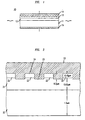
- FIG. 1 is a high-level schematic representation of a QC-DFB laser.
- FIG. 2 is a schematic representation of the upper confinement region and the upper metallic electrode of an exemplary QC-DFB laser according to the present invention.
- FIGS. 3 and 4 are performance curves for one exemplary embodiment of a QC-DFB laser according to the present invention.
- the embodiment of FIGS. 3 and 4 has a grating period of 0.73 ⁇ m.
- the performance curves are for pulsed operation.
- FIG. 3 shows emission wavelength as a function of heat sink temperature.
- FIG. 4 shows voltage and optical output power as functions of current.
- FIGS. 5 and 6 are performance curves for a second exemplary embodiment of a QC-DFB laser according to the present invention.
- the embodiment of FIGS. 5 and 6 has a grating period of 0.75 ⁇ m.
- the performance curves are for cw operation.
- FIG. 5 shows emission wavelength as a function of heat sink temperature near laser threshold and as a function of drive current at constant 80K heat sink temperature.
- FIG. 6 shows voltage as a function of current at 80K heat sink temperature, and also shows optical output power as a function of current at heat sink temperatures of 60K and 80K.
- FIG. 7 is a schematic diagram of an exemplary point sensing apparatus incorporating a QC-DFB laser such as the laser described herein.
- FIG. 8 is a schematic diagram of an exemplary remote-sensing system incorporating a QC-DFB laser such as the laser described herein.
- FIG. 1 schematically shows an exemplary QC-DFB laser 10.
- Numerals 11-13 refer respectively to the lower confinement region, the QC active region, and the upper confinement region, including a grating on the top surface.
- Numerals 14 and 15 refer to metallization layers. The wavy arrows indicate output radiation.
- An exemplary embodiment of the present invention was configured for nominal laser emission at a wavelength of about 4.5 ⁇ m. We measured tunable emission from the exemplary embodiment over a wavelength range of about 4.60-4.75 ⁇ m.
- the exemplary configuration can be scaled for operation at other wavelengths by suitable adjustments in layer thicknesses, material composition, doping levels, and grating period.
- lower confinement region 11 was a portion of the InP substrate, at a relatively low doping level of about 2 ⁇ 10 17 cm -3 . All doping in the exemplary embodiment was n-type, using silicon.
- QC active region 12 consisted of 26 repeat units, each repeat unit comprising an active region and an injector region.
- the total number of repeat units in an effective laser of the inventive kind may be as few as 1 and as many as about 75. Typical numbers of repeat units lie in the range 25-30.
- the repeat units were embedded in a waveguide core of In 0.53 Ga 0.47 As doped at a relatively low level of 1 ⁇ 10 17 cm -3 and grown lattice-matched to the InP substrate. More details of the QC active region are provided below.
- Upper confinement region 13 consisted of: a lower layer of Al 0.48 In 0.52 As 1.5 ⁇ m thick and doped to 3 ⁇ 10 16 cm -3 overlain by a further layer of Al 0.48 In 0.52 As 0.62 ⁇ m thick and doped to 3 ⁇ 10 17 cm -3 , overlain in turn by the PECL.
- the PECL was formed as a layer of Al 0.48 In 0.52 As 0.15 ⁇ m thick and doped to the relatively high level of 4 ⁇ 10 19 cm -3 .
- Digitally graded transition layers 25-30 nm thick, were grown between bulk-like materials, e.g., between the core region and the InP substrate, and in the transition between InGaAs and AlInAs in the upper cladding region.
- the stack of 26 repeat units was bounded from below by a layer of In 0.53 Ga 0.47 As 0.2 ⁇ m thick, and bounded from above by a layer of In 0.53 Ga 0.47 As 0.22 ⁇ m thick.
- the stack of repeat units began and ended with an injection region. Each repeat unit had the structure listed in Table 1.
- the barrier and well compositions within the repeat units were selected to have lattice strain of opposite sign relative to the InP substrate, so that the accumulated strain for all layers of one repeat unit would effectively be zero.
- a QC laser incorporating such strain engineering is described in U.S. Patent No. 6,023,482, issued to F. Capasso et al. on February 8, 2000 under the title "Article Comprising a Strain-Compensated QC Laser” and commonly assigned herewith.
- the barrier-and-well structure within the active region of each repeat unit is designed to have an upper and a lower carrier-energy level, with transitions between them that result in optical emission at the laser emission wavelength.
- the energy separation between these levels was 278 meV, corresponding to an emission wavelength of about 4.5 ⁇ m.
- the etched grating was subsequently covered with top contact metallization of 30 nm Ti / 300 nm Au.
- FIG. 2 shows, in schematic fashion, the upper confinement region and the upper metallic electrode of the exemplary QC-DFB laser.
- Layer 20 is AlInAs doped to 3 ⁇ 10 16 cm -3 and 1.5 ⁇ m thick.
- Layer 21, as noted above, is AlInAs doped to 3 ⁇ 10 17 cm -3 and 0.62 ⁇ m thick (before etching).
- Layer 22, as noted above, is the PECL, made of AlInAs doped to 4 ⁇ 10 19 cm -3 and 0.15 ⁇ m thick before etching.
- Layer 23 is the upper metallic electrode.
- a grating is etched entirely through layer 22 and partway into layer 21.
- the grating includes ridge portions 24 and valley (or "groove") portions 25. Material has been removed from the valley portions by etching. As seen in the figure, the valley portions have been filled with electrode material. The precise manner of filling in the valleys is conventional and need not be described here in detail.
- One effect of the PECL is to reduce the amplitude of the guided waveguide mode of the laser in portions of the upper cladding region that lie adjacent electrode 23. This is an important effect because when the guided mode has appreciable amplitude at the interface between the upper cladding and the electrode, a significant amount of optical loss is brought about by energy dissipation within the electrode material, and similarly the mode is pulled toward the surface (the electrode) and out of the active waveguide core.
- U.S. Patent No. 5,901,168 also discloses a highly doped top cladding layer.
- the top cladding layer is made of InP doped to 7 ⁇ 10 18 cm -3 and 0.90 ⁇ m thick.
- a grating for distributed feedback is etched to a depth of 0.25 ⁇ m in the top cladding layer.
- the coupling constant ⁇ (a quantity describing the strength of the feedback provided by the grating) was estimated to be about 2-3 cm -1 .
- top cladding layer is, respectively, 0.60- ⁇ m AlInAs doped to 7 ⁇ 10 18 cm -3 , and 1.30- ⁇ m InP doped to 7 ⁇ 10 18 cm -3 .
- the latter was a structure with a buried grating.
- the combination of PECL and grating is coupled more strongly to the optical mode than has been hitherto disclosed, and as a consequence achieves substantially stronger modulation at least of the real part of the refractive index, and typically also of the imaginary part.
- the stronger coupling that we achieve is due, at least in part, to the fact that our grating is etched deeply into the PECL, and typically is etched all the way through as shown in the figure.
- the stronger coupling is the direct result of substantially removing the PECL material from the grating grooves or valleys. Material must either be entirely removed or else made so thin in the groove regions that it can no longer function as a separation layer between the mode and the metal electrode. Therefore, the choice of thickness is guided by the feasible, and preferably the readily achievable, etch-depth. The latter depends on the etching technique used and also on the grating period. By way of example, etch depths of about 0.3 ⁇ m are readily achievable by wet chemical etching when the grating period is approximately 1 ⁇ m.
- a smaller etch-depth i.e., about 0.2 ⁇ m or less
- wet-etching This consideration led us to choose a PECL thickness of 0.15 ⁇ m.
- the smaller thickness of the PECL relative to previous QC-lasers had to be compensated by a higher doping level (the exact value also being influenced by the laser wavelength), to make it effective in the locations near the inter-groove mid-points.
- doping levels sufficient to achieve such compensation are readily determinable from analytical formulas and numerical modeling.
- the guided waveguide mode in valleys 25 couples strongly to the metal-semiconductor interface plasmon. This tends to increase the waveguide attenuation coefficient at the valley positions relative to the same coefficient at the positions of ridges 24, where the coupling to the plasmon is suppressed. This also tends to enhance the modal amplitude within the PECL, which induces substantial modulation of the modal effective refractive index and the modal confinement factor.
- the modal confinement factor is a measure of the overlap of the optical mode with the active regions and injectors, and it is intended to be higher in regions of relatively high gain and lower in regions of relatively low gain.
- the modulation n 1 of the real part of the refractive index to be about 452 ⁇ 10 -3 and the modulation amplitude ⁇ 1 of the absorption coefficient for the laser guided mode to be about 12.8 cm -1 .
- Our estimate of the corresponding modulation amplitude ⁇ 1 of the modal confinement factor is 0.21.
- the modulation amplitude n 1 of the effective refractive index is at least 1 ⁇ 10 -3 , and preferably even higher.
- the valleys of the grating are etched sufficiently deeply into the PECL.
- the valleys will be etched through at least 85% of the PECL thickness.
- the thickness of the PECL is primarily chosen such that etching through the layer is readily achievable.
- FIGS. 3 and 4 show the performance of an 11 ⁇ m wide and 2.25 mm long QC-DFB laser device made substantially as described here with a grating period of 0.73 ⁇ m, and operated in pulsed mode with a 50-ns pulse width and 5-kHz repetition rate.
- FIG. 3 shows the emission wavelength as a function of heat sink temperature. The solid circles are obtained from spectra close to threshold, and the open circles at approximately twice the threshold current.
- FIG. 4 shows voltage (dashed curve) and optical output power (solid curve) as functions of current. Optical power curves are given for several heat sink temperatures. Light output was collected with approximately 60% collection efficiency from one facet. The laser was single-mode for all current levels shown.
- Reliable single-mode output was achieved in the temperature range 90K-300K.
- a side mode suppression ratio of about 30 dB was achieved independent of the current level.
- a peak power level of 100 mW was achieved at room temperature.
- a slope efficiency of 180 mW/A was achieved at room temperature and a slope efficiency of 400 mW/A was achieved at low temperatures.
- the threshold current density at room temperature in pulsed operation was 7 kA/cm 2 , and the T 0 value was 113K.
- T 0 can be found in C. Gmachl et al., Appl. Phys. Lett. 72 (1998) 1430-1432, cited above.
- FIGS. 5 and 6 show the performance of a 9 ⁇ m wide laser made substantially as described here with a grating period of 0.75 ⁇ m and operated cw and single mode.
- FIG. 5 shows the emission wavelength as a function of the heat sink temperature close to laser threshold (triangles) and as a function of drive current at a constant heat sink temperature of 80K (circles).
- FIG. 6 shows the voltage (dashed curve) as a function of current at a heat sink temperature of 80K, and also shows the optical output power as a function of current at heat sink temperatures of 60K and 80K.
- the maximum cw single-mode output power at 80K was 150 mW, the slope efficiency was less than or equal to 400 mW/A, and the threshold current density was 3.5 kA/cm 2 .
- QC-DFB lasers can advantageously be used in point sensing apparatus and in remote sensing apparatus for spectral analysis and detection of many substances, particularly gaseous substances, having infrared spectral features.
- Numerous well-known instrumental configurations incorporating a QC-DFB laser are useful in this regard. Without limitation, such configurations include wavelength modulation, direct absorption, photoacoustic cell (PAC), and cavity ring down (CRD) configurations.
- PAC photoacoustic cell
- CCD cavity ring down
- FIG. 7 schematically depicts exemplary point sensing apparatus 70, wherein numeral 71 refers to a QC-DFB laser according to the invention.
- the QC-DFB laser of FIG. 7 is configured for wavelength modulation.
- the laser is mounted on a temperature-controlled stage (not shown) for coarse wavelength tuning.
- Mid-IR radiation 721 from the laser passes through conventional gas cell 73 (optionally a multi-pass cell), with exited radiation 722 impinging on conventional detector 74.
- the electrical output of the detector is supplied to lock-in amplifier 75 (together with an appropriate modulation signal, e.g., a 1.2 kHz sine wave from modulation signal generator 783), and the lock-in amplifier output is supplied to computer 76 for data analysis and formatting.
- an appropriate modulation signal e.g., a 1.2 kHz sine wave from modulation signal generator 783
- the data are then displayed and stored in any suitable manner.
- the QC-DFB laser is pumped with an appropriate electrical current.
- a low frequency current ramp having, e.g., a 250-ms period
- short bias pulses e.g., of a 5-ns pulse width and 2- ⁇ s period
- modulation signal from modulation current generator 783 are supplied to combiner 73, and the resultant current ramp with superimposed current pulses and sine wave is applied to the laser.
- the current ramp serves to sweep the laser temperature over a predetermined range, and the pulses cause the emission of short laser pulses.
- the pulse wavelength is slowly swept over a range of wavelengths, and absorption as a function of wavelength is determined.
- the presence in the cell of a gas that has an absorption line in the range of wavelengths is readily detected, and the gas can be identified.
- some conventional features are not shown in FIG. 7. For instance, the measurement set-up will typically be under computer control, requiring further inputs to, and outputs from, the computer.
- FIG. 8 schematically depicts an exemplary remote-sensing system 80, wherein emission source 81 (e.g., a factory exhaust stack) emits gaseous emission cloud 82.
- emission source 81 e.g., a factory exhaust stack
- QC-DFB laser 83 emits mid-IR radiation 84 which propagates through the emission cloud, and is reflected, exemplarily by a corner reflector 85.
- Reflected radiation 87 is then detected by detector 88.
- the laser can be pumped in any appropriate manner, e.g., as described in conjunction with FIG. 7, and the detector output can be utilized in any appropriate manner, e.g., also as described above.
- a mirror or other appropriate reflector can be used instead of corner reflector 85.
- the reflector can be on an aircraft or any elevated feature, including the exhaust stack that is being monitored. Of course, the detector could also be on an aircraft or elevated feature. In general, any arrangement that results in a line-of-sight disposition of laser and detector is contemplate
- the QC-DFB laser will generally be mounted in an appropriate housing for protection and control.
- the package will typically comprise cooling means (e.g., water cooling, thermoelectric cooling), temperature sensor means (e.g., a thermocouple) for use in a feedback loop for temperature control, and means for applying the pump current to the laser.
- the laser is attached in conventional fashion to the cooling means.
- the housing may also contain detector means for controlling laser output power.
- the housing will typically have a window that is transparent for the laser radiation, and will typically be evacuated or filled with inert gas.
Landscapes
- Physics & Mathematics (AREA)
- Optics & Photonics (AREA)
- Condensed Matter Physics & Semiconductors (AREA)
- General Physics & Mathematics (AREA)
- Electromagnetism (AREA)
- Chemical & Material Sciences (AREA)
- Engineering & Computer Science (AREA)
- Nanotechnology (AREA)
- Life Sciences & Earth Sciences (AREA)
- Biophysics (AREA)
- Crystallography & Structural Chemistry (AREA)
- Semiconductor Lasers (AREA)
Abstract
Description
- This invention pertains to quantum cascade (QC) lasers, and to apparatus and systems that comprise a QC laser. More particularly, the invention pertains to quantum cascade distributed feedback (QC-DFB) lasers.
- QC lasers are unipolar semiconductor lasers that can be designed to emit light over a tunable range of infrared (IR) wavelengths. In particular, such lasers can be designed to emit in the mid-IR spectral region from about 3 µm to about 17 µ m. This spectral range is important because, inter alia, absorption lines of many industrial gases and environmental pollutants lie therein. This suggests that QC lasers may have advantageous applications as radiation sources for absorption spectroscopy of such substances in, e.g., sensors for environmental surveys or process control.
- A QC laser has a multilayer structure that forms an optical waveguide, including a core region of relatively large effective refractive index disposed between lower and upper cladding regions of relatively small effective refractive index. A cladding region is also referred to as a "confinement" region because the guided optical radiation tends to be confined within the higher-index region, i.e., within the core, whose boundaries are marked by the transition to the lower-index cladding regions.
- The core region comprises a multiplicity of nominally identical repeat units, with each repeat unit comprising an active region and a carrier injector region. The active region has a layer structure selected to provide an upper and a lower energy state for carriers, which are typically electrons but may alternatively be holes. The separation between the upper and lower states is such that a carrier transition from the upper to the lower state may result in emission of a photon at an infrared wavelength λ.
- The carrier injector region has a layer structure selected to facilitate the transport of carriers occupying the lower energy state of the active region of a given repeat unit to the active region of the adjacent, downstream repeat unit, such that the transported carriers will occupy the upper energy state of the downstream active region. A carrier thus undergoes successive transitions from an upper to a lower energy state as the carrier moves through the layer structure, meanwhile emitting multiple photons of wavelength λ. The photon energy, and thus the wavelength λ, depends on the structural and compositional details of the repeat units.
- One desirable property of QC lasers, particularly in applications involving precise spectroscopic measurements, is single-mode operation, as defined by a suppression of side modes by a factor of typical order 1000 (in measurements of the optical power). Early QC lasers were incapable of single-mode emission in continuous wave (cw) operation at cryogenic temperatures (below about 140 K) and in pulsed operation at room temperature. Typical emission spectra of QC-lasers are multiple-mode.
- U.S. Patent No. 5,901,168, which issued on April 27, 1999 to J.N. Baillargeon et al. under the title "Article Comprising an Improved QC Laser" and is commonly assigned herewith, describes an improved QC laser capable of single-mode operation . The single-mode operation was achieved through the use of a grating structure for providing distributed feedback. The grating structure was specifically designed to induce single-mode operation. Because a grating structure was used for distributed feedback, the laser described there belonged to the class referred to as QC-DFB lasers.
- Significantly, the benefits of single-mode emission were achieved in U.S. Patent No. 5,901,168 using a grating structure fabricated on the upper surface of the device, and not a buried grating structure formed adjacent the core layer (although the cited patent also reported on results obtained using such a buried structure). The use of an overlying, and not a buried, grating structure is advantageous because it substantially simplifies the fabrication process. However, because of greater separation from the core layer, an overlying grating structure has generally been believed to offer weaker coupling of the optical mode to the grating than a buried grating structure, and consequently to have a weaker effect. In particular, coupling via a modulation by a surface grating of the effective refractive index of the modes was believed to be inefficient. In fact, early QC-DFB lasers fabricated with surface gratings did not operate in grating-induced single-mode emission when operated in cw. The latter requires a strong coupling between the guided mode and the grating.
- There remains a need for QC-DFB lasers having still higher output powers and, in particular, operable with single-mode cw output. However, mode instability tends to be aggravated as temperatures and power levels increase. Strongly mode-coupled structures are needed to counter such spectral instability. Thus, one recognized problem in the art has been to provide mode stabilization sufficient to extend the range of single-mode operation with respect to optical output power and possibly operating temperature, particularly for cw conditions, while continuing to enjoy the convenience afforded to the fabrication process by using overlying, rather than buried, grating structures.
- We have devised an overlying grating structure that achieves relatively strong coupling of the guided mode to the grating, and is thus highly effective in inducing a QC-DFB laser for single-mode operation even under cw operating conditions. Using such a grating structure, we have demonstrated continuously tunable, pulsed, single-mode operation at room temperature, and the first grating-induced continuously tunable, cw, single-mode operation at and above liquid nitrogen temperature, i.e., at and above 77K.
- Our invention is embodied in an article (e.g., an absorption spectroscopy system) that comprises a QC-DFB laser. The QC-DFB laser comprises first and second cladding regions and a core region disposed between them. The core region comprises a multiplicity of multilayer semiconductor repeat units selected for lasing at a wavelength λ. The QC-DFB laser further comprises a grating structure for providing distributed feedback to facilitate single-mode laser operation. The grating structure overlies the core and is separated therefrom by at least a portion of the upper cladding region. The grating structure is overlain by an upper metallic electrode.
- At least part of the grating structure is formed as a series of grooves (also referred to herein as "valleys") etched in a semiconductor layer, denominated the plasmon-enhanced confinement layer (PECL), which is disposed adjacent and in contact with the upper metallic electrode. The refractive index of the PECL at the lasing wavelength λ is typically significantly lower than the refractive index of any of the cladding layers that underlie it. A guided waveguide mode of the laser will experience an effective refractive index at the midpoint positions of the grooves that is different from the effective refractive index at the midpoint positions between the grooves.
- The thickness, refractive index (as adjusted through doping), and etched depth of the PECL are chosen such that the effective refractive index changes between the intra-groove midpoint positions and the inter-groove midpoint positions by at least 2×10⁻³ and possibly by as much as 1×10⁻² or even more, although a currently preferred value is about 5×10⁻³.
- The properties of the PECL are chosen such that near the intra-groove midpoint positions, where PECL material is substantially or even entirely removed, the laser mode travelling in the waveguide can couple efficiently to the surface-plasmon, which exists at the interface between the upper cladding layers and the overlying electrode. This has the effect of "pulling" the mode toward the surface and thereby changing its overlap with the various layers constituting the waveguide. Near the inter-groove mid-point positions, where the PECL is intact, the coupling to the surface-plasmon is at least partially suppressed, effectively "pushing" the mode away from the surface. This "push-pull" action (periodic with the grating period) is responsible for a relatively strong modulation of the refractive index. Secondarily, it also induces a modulation of the modal gain via a modulation of the confinement factor, defined as the overlap of the guided mode with the waveguide core, i.e., with the multiplicity of active regions and injectors. (It should be noted that the spatially modulated coupling to the inherently lossy surface-plasmon furthermore induces a loss modulation.)
- A "push" or "pull" of the laser mode refers to a relative decrease or increase, respectively, in amplitude of the electromagnetic field of the laser radiation near the feature of interest, i.e.,. the PECL or grating. The amount of "push-pull" can be quantified by the change in confinement factor, and is preferably designed to be approximately 10% - 20% (as absolute percentages of the waveguide confinement), but can be made even higher if desired.
- FIG. 1 is a high-level schematic representation of a QC-DFB laser.
- FIG. 2 is a schematic representation of the upper confinement region and the upper metallic electrode of an exemplary QC-DFB laser according to the present invention.
- FIGS. 3 and 4 are performance curves for one exemplary embodiment of a QC-DFB laser according to the present invention. The embodiment of FIGS. 3 and 4 has a grating period of 0.73 µm. The performance curves are for pulsed operation. FIG. 3 shows emission wavelength as a function of heat sink temperature. FIG. 4 shows voltage and optical output power as functions of current.
- FIGS. 5 and 6 are performance curves for a second exemplary embodiment of a QC-DFB laser according to the present invention. The embodiment of FIGS. 5 and 6 has a grating period of 0.75 µm. The performance curves are for cw operation. FIG. 5 shows emission wavelength as a function of heat sink temperature near laser threshold and as a function of drive current at constant 80K heat sink temperature. FIG. 6 shows voltage as a function of current at 80K heat sink temperature, and also shows optical output power as a function of current at heat sink temperatures of 60K and 80K.
- FIG. 7 is a schematic diagram of an exemplary point sensing apparatus incorporating a QC-DFB laser such as the laser described herein.
- FIG. 8 is a schematic diagram of an exemplary remote-sensing system incorporating a QC-DFB laser such as the laser described herein.
- FIG. 1 schematically shows an exemplary QC-
DFB laser 10. Numerals 11-13 refer respectively to the lower confinement region, the QC active region, and the upper confinement region, including a grating on the top surface.Numerals 14 and 15 refer to metallization layers. The wavy arrows indicate output radiation. - An exemplary embodiment of the present invention was configured for nominal laser emission at a wavelength of about 4.5 µm. We measured tunable emission from the exemplary embodiment over a wavelength range of about 4.60-4.75µm. As will be appreciated by those skilled in the art, the exemplary configuration can be scaled for operation at other wavelengths by suitable adjustments in layer thicknesses, material composition, doping levels, and grating period. In the exemplary embodiment,
lower confinement region 11 was a portion of the InP substrate, at a relatively low doping level of about 2 ×1017 cm-3. All doping in the exemplary embodiment was n-type, using silicon. - QC
active region 12 consisted of 26 repeat units, each repeat unit comprising an active region and an injector region. The total number of repeat units in an effective laser of the inventive kind may be as few as 1 and as many as about 75. Typical numbers of repeat units lie in the range 25-30. The repeat units were embedded in a waveguide core of In0.53Ga0.47As doped at a relatively low level of 1×1017 cm-3 and grown lattice-matched to the InP substrate. More details of the QC active region are provided below. -
Upper confinement region 13 consisted of: a lower layer of Al0.48In0.52As 1.5 µm thick and doped to 3×1016 cm-3 overlain by a further layer of Al0.48In0.52As 0.62 µm thick and doped to 3×1017 cm-3, overlain in turn by the PECL. The PECL was formed as a layer of Al0.48In0.52As 0.15 µm thick and doped to the relatively high level of 4×1019 cm-3. - Digitally graded transition layers, 25-30 nm thick, were grown between bulk-like materials, e.g., between the core region and the InP substrate, and in the transition between InGaAs and AlInAs in the upper cladding region.
- Within the QC active region, the stack of 26 repeat units was bounded from below by a layer of In0.53Ga0.47As 0.2 µm thick, and bounded from above by a layer of In0.53Ga0.47As 0.22 µm thick. The stack of repeat units began and ended with an injection region. Each repeat unit had the structure listed in Table 1.
- The barrier and well compositions within the repeat units were selected to have lattice strain of opposite sign relative to the InP substrate, so that the accumulated strain for all layers of one repeat unit would effectively be zero. A QC laser incorporating such strain engineering is described in U.S. Patent No. 6,023,482, issued to F. Capasso et al. on February 8, 2000 under the title "Article Comprising a Strain-Compensated QC Laser" and commonly assigned herewith.
- As mentioned above, the barrier-and-well structure within the active region of each repeat unit is designed to have an upper and a lower carrier-energy level, with transitions between them that result in optical emission at the laser emission wavelength. At the design electric field of 70 kV/cm, the energy separation between these levels was 278 meV, corresponding to an emission wavelength of about 4.5 µm.
- The grating, which was designed to be a first-order Bragg-grating, was fabricated by optical contact lithography, O2 plasma processing of the resist grating, and wet etching in HBr: HNO3 : H2O = 1 : 1: 10 to a depth of approximately 0.20 µm. This etch depth was sufficient to entirely remove the PECL material from the valley portions of the grating. The etched grating was subsequently covered with top contact metallization of 30 nm Ti / 300 nm Au.
- We cleaved the lasers to a length of 2.25 mm, which would theoretically yield a coupling product (i.e., coupling coefficient times length) of 3.6, a target design value which has previously been shown to yield reliable single-mode QC-DFB lasers. Stripe widths were 8-11 µm.
- The laser processing and measurement procedures were conventional, and are described, for example, in the article by C. Gmachl et al., "Continuous-wave and high-power pulsed operation of index-coupled distributed feedback quantum cascade laser at λ ≈ 8.5 µm," Appl. Phys. Lett. 72 (1998) 1430-1432.
- FIG. 2 shows, in schematic fashion, the upper confinement region and the upper metallic electrode of the exemplary QC-DFB laser.
Layer 20, as noted above, is AlInAs doped to 3×1016 cm-3 and 1.5 µm thick.Layer 21, as noted above, is AlInAs doped to 3×1017 cm-3 and 0.62 µm thick (before etching).Layer 22, as noted above, is the PECL, made of AlInAs doped to 4×1019 cm-3 and 0.15 µm thick before etching.Layer 23 is the upper metallic electrode. As shown in the figure, a grating is etched entirely throughlayer 22 and partway intolayer 21. The grating includesridge portions 24 and valley (or "groove")portions 25. Material has been removed from the valley portions by etching. As seen in the figure, the valley portions have been filled with electrode material. The precise manner of filling in the valleys is conventional and need not be described here in detail. - One effect of the PECL is to reduce the amplitude of the guided waveguide mode of the laser in portions of the upper cladding region that lie
adjacent electrode 23. This is an important effect because when the guided mode has appreciable amplitude at the interface between the upper cladding and the electrode, a significant amount of optical loss is brought about by energy dissipation within the electrode material, and similarly the mode is pulled toward the surface (the electrode) and out of the active waveguide core. - It has been known in the past that a PECL is useful for suppressing optical amplitude at that semiconductor-metal interface. For example, U.S. Patent No. 5,502,787, issued to F. Capasso et al. on March 26, 1996 under the title "Article Comprising a Semiconductor Waveguide Structure" and commonly assigned herewith, describes a QC laser (without distributed feedback) having a top cladding layer of GaInAs doped to 7 × 1018 cm-3 and 0.60 µm thick. Patent 5,502,787 provides formulas for deriving the real and imaginary parts of the refractive index from basic physical properties of the layer material, the doping level, and the pertinent optical wavelength. The same patent shows that for a given layer composition, there is a range of doping levels within which the real and imaginary parts of the refractive index are both relatively low. It is important to have a low real part of the refractive index to provide the desired optical confinement within the cladding and away from the electrode interface. It is important to have a low imaginary part in order to avoid excessive optical loss.
- U.S. Patent No. 5,901,168, cited above, also discloses a highly doped top cladding layer. There, the top cladding layer is made of InP doped to 7×1018 cm-3 and 0.90 µm thick. A grating for distributed feedback is etched to a depth of 0.25 µm in the top cladding layer. The coupling constant κ (a quantity describing the strength of the feedback provided by the grating) was estimated to be about 2-3 cm-1.
- Alternate structures are disclosed in Patent No. 5,901,168, in which the top cladding layer is, respectively, 0.60-µm AlInAs doped to 7×1018 cm-3, and 1.30-µm InP doped to 7×1018 cm-3. The latter was a structure with a buried grating.
- In our new structure, such as the structure illustrated in FIG. 2, the combination of PECL and grating is coupled more strongly to the optical mode than has been hitherto disclosed, and as a consequence achieves substantially stronger modulation at least of the real part of the refractive index, and typically also of the imaginary part. The stronger coupling that we achieve is due, at least in part, to the fact that our grating is etched deeply into the PECL, and typically is etched all the way through as shown in the figure.
- The stronger coupling is the direct result of substantially removing the PECL material from the grating grooves or valleys. Material must either be entirely removed or else made so thin in the groove regions that it can no longer function as a separation layer between the mode and the metal electrode. Therefore, the choice of thickness is guided by the feasible, and preferably the readily achievable, etch-depth. The latter depends on the etching technique used and also on the grating period. By way of example, etch depths of about 0.3 µm are readily achievable by wet chemical etching when the grating period is approximately 1 µm.
- In the present exemplary embodiment, with a grating period of approximately 0.75 µm, a smaller etch-depth (i.e., about 0.2 µm or less) is readily achievable by wet-etching. This consideration led us to choose a PECL thickness of 0.15 µm. Significantly, the smaller thickness of the PECL relative to previous QC-lasers had to be compensated by a higher doping level (the exact value also being influenced by the laser wavelength), to make it effective in the locations near the inter-groove mid-points. Those skilled in the art will appreciate that doping levels sufficient to achieve such compensation are readily determinable from analytical formulas and numerical modeling.
- By way of example, it will be typical for lasers emitting in the range 4-5 µm to have a PECL less than 0.25 µm thick, and doped to a concentration of at least 1×1019 cm-3. Similarly, it will be typical for lasers emitting in the range 9-10 µm to have a PECL less than 0.35 µm thick, and doped to a concentration of at least 8×1018 cm-3.
- Turning again to FIG. 2, the guided waveguide mode in
valleys 25 couples strongly to the metal-semiconductor interface plasmon. This tends to increase the waveguide attenuation coefficient at the valley positions relative to the same coefficient at the positions ofridges 24, where the coupling to the plasmon is suppressed. This also tends to enhance the modal amplitude within the PECL, which induces substantial modulation of the modal effective refractive index and the modal confinement factor. As will be understood by those skilled in the art, the modal confinement factor is a measure of the overlap of the optical mode with the active regions and injectors, and it is intended to be higher in regions of relatively high gain and lower in regions of relatively low gain. For our exemplary structure, we estimate the modulation n 1 of the real part of the refractive index to be about 452 × 10-3 and the modulation amplitude α 1 of the absorption coefficient for the laser guided mode to be about 12.8 cm-1. Our estimate of the corresponding modulation amplitude Γ1 of the modal confinement factor is 0.21. - We have estimated the resulting coupling coefficient K of the grating to be about 16 cm-1. In comparison, prior art top-grating devices reached K of only about 2-3 cm-1. By contrast, lasers made according to the present invention will typically have K equal to 10 cm-1 or more.
- The dominant contribution to the coupling coefficient achieved in the present exemplary embodiment of the invention, by roughly a factor of four, is the modulation of the effective refractive index. To achieve the advantages of our new grating-PECL structure, it will generally be desirable for the modulation amplitude n 1 of the effective refractive index to be at least 1×10⁻³, and preferably even higher. This is readily achievable, provided the valleys of the grating are etched sufficiently deeply into the PECL. In typical lasers made according to the present invention, the valleys will be etched through at least 85% of the PECL thickness. In at least some cases, it will, in fact, be preferable to etch through 100% of the PECL thickness. As previously stated, the thickness of the PECL is primarily chosen such that etching through the layer is readily achievable.
- FIGS. 3 and 4 show the performance of an 11 µm wide and 2.25 mm long QC-DFB laser device made substantially as described here with a grating period of 0.73 µm, and operated in pulsed mode with a 50-ns pulse width and 5-kHz repetition rate. FIG. 3 shows the emission wavelength as a function of heat sink temperature. The solid circles are obtained from spectra close to threshold, and the open circles at approximately twice the threshold current. FIG. 4 shows voltage (dashed curve) and optical output power (solid curve) as functions of current. Optical power curves are given for several heat sink temperatures. Light output was collected with approximately 60% collection efficiency from one facet. The laser was single-mode for all current levels shown.
- Reliable single-mode output was achieved in the temperature range 90K-300K. In single-mode operation, a side mode suppression ratio of about 30 dB was achieved independent of the current level. A peak power level of 100 mW was achieved at room temperature. A slope efficiency of 180 mW/A was achieved at room temperature and a slope efficiency of 400 mW/A was achieved at low temperatures. The threshold current density at room temperature in pulsed operation was 7 kA/cm2, and the T0 value was 113K. A definition of T0 can be found in C. Gmachl et al., Appl. Phys. Lett. 72 (1998) 1430-1432, cited above.
- FIGS. 5 and 6 show the performance of a 9 µm wide laser made substantially as described here with a grating period of 0.75 µm and operated cw and single mode. FIG. 5 shows the emission wavelength as a function of the heat sink temperature close to laser threshold (triangles) and as a function of drive current at a constant heat sink temperature of 80K (circles). FIG. 6 shows the voltage (dashed curve) as a function of current at a heat sink temperature of 80K, and also shows the optical output power as a function of current at heat sink temperatures of 60K and 80K.
- In cw operation, our linewidth measurement was limited by the resolution of the spectrometer, which was approximately 7.5 GHz.
- The maximum cw single-mode output power at 80K was 150 mW, the slope efficiency was less than or equal to 400 mW/A, and the threshold current density was 3.5 kA/cm2.
- In general, QC-DFB lasers can advantageously be used in point sensing apparatus and in remote sensing apparatus for spectral analysis and detection of many substances, particularly gaseous substances, having infrared spectral features. Numerous well-known instrumental configurations incorporating a QC-DFB laser are useful in this regard. Without limitation, such configurations include wavelength modulation, direct absorption, photoacoustic cell (PAC), and cavity ring down (CRD) configurations. Published descriptions of spectroscopic instruments incorporating QC-DFB lasers include: R.M. Williams et al., "Kilohertz linewidth from frequency-stabilized mid-infrared quantum cascade lasers," Optics Letters 24 (1999) 1844-1846; B.A. Paldus et al., "Photoacoustic spectroscopy using quantum-cascade lasers," Optics Letters 24 (1999) 178-180; A.A. Kosterev et al., "Methane concentration and isotopic composition measurements with a mid-infrared quantum-cascade laser," Optics Letters 24 (1999) 1762-1764; and K. Namjou et al., "Sensitive absorption spectroscopy with a room-temperature distributed-feedback quantum-cascade laser," Optics Letters 23 (1998) 219-221.
- FIG. 7 schematically depicts exemplary
point sensing apparatus 70, wherein numeral 71 refers to a QC-DFB laser according to the invention. For purposes of illustration, the QC-DFB laser of FIG. 7 is configured for wavelength modulation. Typically the laser is mounted on a temperature-controlled stage (not shown) for coarse wavelength tuning.Mid-IR radiation 721 from the laser passes through conventional gas cell 73 (optionally a multi-pass cell), with exitedradiation 722 impinging onconventional detector 74. The electrical output of the detector is supplied to lock-in amplifier 75 (together with an appropriate modulation signal, e.g., a 1.2 kHz sine wave from modulation signal generator 783), and the lock-in amplifier output is supplied tocomputer 76 for data analysis and formatting. The data are then displayed and stored in any suitable manner. The QC-DFB laser is pumped with an appropriate electrical current. For instance, a low frequency current ramp (having, e.g., a 250-ms period) from rampcurrent generator 781, short bias pulses (e.g., of a 5-ns pulse width and 2-µs period) from biascurrent generator 782, and a modulation signal from modulationcurrent generator 783 are supplied tocombiner 73, and the resultant current ramp with superimposed current pulses and sine wave is applied to the laser. The current ramp serves to sweep the laser temperature over a predetermined range, and the pulses cause the emission of short laser pulses. The pulse wavelength is slowly swept over a range of wavelengths, and absorption as a function of wavelength is determined. Thus, the presence in the cell of a gas that has an absorption line in the range of wavelengths is readily detected, and the gas can be identified. As those skilled in the art will recognize, some conventional features are not shown in FIG. 7. For instance, the measurement set-up will typically be under computer control, requiring further inputs to, and outputs from, the computer. - FIG. 8 schematically depicts an exemplary remote-sensing
system 80, wherein emission source 81 (e.g., a factory exhaust stack) emits gaseous emission cloud 82. QC-DFB laser 83 emits mid-IR radiation 84 which propagates through the emission cloud, and is reflected, exemplarily by a corner reflector 85. Reflected radiation 87 is then detected by detector 88. The laser can be pumped in any appropriate manner, e.g., as described in conjunction with FIG. 7, and the detector output can be utilized in any appropriate manner, e.g., also as described above. A mirror or other appropriate reflector can be used instead of corner reflector 85. The reflector can be on an aircraft or any elevated feature, including the exhaust stack that is being monitored. Of course, the detector could also be on an aircraft or elevated feature. In general, any arrangement that results in a line-of-sight disposition of laser and detector is contemplated. - The QC-DFB laser will generally be mounted in an appropriate housing for protection and control. The package will typically comprise cooling means (e.g., water cooling, thermoelectric cooling), temperature sensor means (e.g., a thermocouple) for use in a feedback loop for temperature control, and means for applying the pump current to the laser. The laser is attached in conventional fashion to the cooling means. Optionally, the housing may also contain detector means for controlling laser output power. The housing will typically have a window that is transparent for the laser radiation, and will typically be evacuated or filled with inert gas.
Layer Type Thickness (nm) Sub-Region Doping Level Barrier 4.4 Active Well 0.9 Active Barrier 0.9 Active Well 4.8 Active Barrier 1.7 Active Well 4.4 Active Barrier 2.8 Active Well 3.4 Injection Barrier 1.2 Injection Well 3.1 Injection Barrier 1.4 Injection Well 2.8 Injection 3×1017 cm-3 Barrier 1.6 Injection Well 2.8 Injection 3×1017 cm-3 Barrier 2.0 Injection Well 2.5 Injection 3×1017 cm-3 Barrier 2.3 Injection Well 2.3 Injection Barrier 2.8 Injection Well 2.1 Injection Barrier 3.0 Injection Well 1.9 Injection
Claims (16)
- Apparatus comprising a quantum cascade, distributed feedback laser having lower and upper cladding regions and a core region, said regions collectively adapted to guide at least one mode of laser radiation, wherein:(a) the upper cladding region includes a layer, denominated the plasmon-enhanced confinement layer (PECL), that overlies at least one further layer of the upper cladding region and adjacently underlies a metallic electrode;(b) a grating structure is formed as a series of grooves in the PECL;(c) the PECL is conformed such that during laser operation, the amplitude of the guided laser mode is relatively enhanced within first portions of the upper cladding region underlying said grooves but is relatively suppressed within second portions of the upper cladding region lying between said first portions, said enhancement and suppression resulting in a modulation of the guided laser mode; and(d) said modulation is strong enough to facilitate single-mode cw laser operation.
- Apparatus of claim 1, wherein the PECL has a layer thickness, and the grooves extend to a depth that is a substantial fraction of the PECL layer thickness.
- Apparatus of claim 2, wherein the grooves extend to a depth that is at least 85% of the PECL layer thickness.
- Apparatus of claim 2, wherein the grooves extend entirely through the PECL.
- Apparatus of claim 1, wherein said laser radiation has a wavelength in the range 4.60-4.75 µm.
- Apparatus of claim 1, wherein the apparatus is a measurement system for measuring infrared absorption by a target species, wherein:the measurement system comprises a source of single-mode infrared laser radiation and a detector for detecting said radiation after it has interacted with a quantity of said target species; andsaid source comprises the quantum cascade, distributed feedback laser ofclaim 1.
- The measurement system of claim 6, wherein the target species is a gas disposed in a measurement cell.
- The measurement system of claim 6, wherein the target species is an unconfined gas.
- Apparatus of claim 1, further comprising a current source electrically connected to said laser so as to provide a laser-heating current to the laser, such that the laser radiation will vary in wavelength as the laser-heating current is varied.
- Apparatus of claim 1, wherein the modulation of the guided laser mode is strong enough to facilitate single-mode cw laser operation at a laser temperature of at least 77K.
- Apparatus comprising a quantum cascade, distributed feedback laser having lower and upper cladding regions and a core region, said regions collectively adapted to guide at least one mode of laser radiation, wherein:(a) the upper cladding region includes a layer, denominated the plasmon-enhanced confinement laser (PECL), that overlies at least one further layer of the upper cladding region and adjacently underlies a metallic electrode;(b) a grating structure is formed as a series of grooves in the PECL;(c) during laser operation, the guided laser mode experiences an effective refractive index; and(d) the PECL is conformed so as to modulate said effective refractive index with a modulation amplitude of at least 2×10⁻³.
- Apparatus comprising a quantum cascade, distributed feedback laser having lower and upper cladding regions and a core region, said regions collectively adapted to guide at least one mode of laser radiation, wherein:(a) the upper cladding region includes a layer, denominated the plasmon-enhanced confinement laser (PECL), that overlies at least one further layer of the upper cladding region and adjacently underlies a metallic electrode;(b) a grating structure is formed as a series of grooves in the PECL;(c) during laser operation, the guided laser mode has a degree of overlap with the core region that is quantifiable in terms of a confinement factor; and(d) the PECL is conformed so as to modulate the confinement factor with a modulation amplitude of at least 10%.
- Apparatus comprising a quantum cascade, distributed feedback laser having lower and upper cladding regions and a core region, said regions collectively adapted to guide at least one mode of laser radiation, wherein:(a) the upper cladding region includes a layer, denominated the plasmon-enhanced confinement laser (PECL), that overlies at least one further layer of the upper cladding region and adjacently underlies a metallic electrode;(b) a grating structure is formed as a series of grooves in the PECL;(c) the grating structure is selected to provide distributed optical feedback during laser operation, said feedback quantifiable by a coupling constant; and(d) the PECL is conformed to provide a coupling constant of at least 10 cm-1.
- Apparatus comprising a quantum cascade, distributed feedback laser having lower and upper cladding regions and a core region, said regions collectively adapted to guide at least one mode of laser radiation, wherein:(a) the upper cladding region includes a layer, denominated the plasmon-enhanced confinement laser (PECL), that overlies at least one further layer of the upper cladding region and adjacently underlies a metallic electrode;(b) a grating structure is formed as a series of grooves in the PECL;(c) the PECL has a layer thickness and dopant concentration selected to suppress the amplitude of the guided laser mode near the metallic electrode; and(d) the grooves extend to a depth that is a substantial fraction of the PECL layer thickness.
- Apparatus of claim 14, wherein the grooves extend to a depth that is at least 85% of the PECL layer thickness.
- Apparatus of claim 14, wherein the PECL layer thickness is less than 0.35 µm, and the PECL dopant concentration is at least 8×1018 cm-3.
Applications Claiming Priority (2)
| Application Number | Priority Date | Filing Date | Title |
|---|---|---|---|
| US09/512,757 US6400744B1 (en) | 2000-02-25 | 2000-02-25 | Apparatus comprising a quantum cascade laser having improved distributed feedback for single-mode operation |
| US512757 | 2000-02-25 |
Publications (2)
| Publication Number | Publication Date |
|---|---|
| EP1137133A1 true EP1137133A1 (en) | 2001-09-26 |
| EP1137133B1 EP1137133B1 (en) | 2004-01-28 |
Family
ID=24040423
Family Applications (1)
| Application Number | Title | Priority Date | Filing Date |
|---|---|---|---|
| EP00307623A Expired - Lifetime EP1137133B1 (en) | 2000-02-25 | 2000-09-04 | Quantum cascade laser having distributed feedback for single-mode cw operation |
Country Status (4)
| Country | Link |
|---|---|
| US (1) | US6400744B1 (en) |
| EP (1) | EP1137133B1 (en) |
| JP (1) | JP3833463B2 (en) |
| DE (1) | DE60007959T2 (en) |
Cited By (4)
| Publication number | Priority date | Publication date | Assignee | Title |
|---|---|---|---|---|
| GB2400233A (en) * | 2003-04-01 | 2004-10-06 | Agilent Technologies Inc | Distributed feedback laser device |
| EP1617471A1 (en) * | 2004-07-13 | 2006-01-18 | Alpes Lasers S.A. | Semiconductor lasers device |
| CN100405681C (en) * | 2006-09-08 | 2008-07-23 | 中国科学院上海微系统与信息技术研究所 | Structure of waveguide and grating of tunable distributed feedback quantum cascade laser and preparation method of said grating |
| EP1990878A1 (en) * | 2007-05-11 | 2008-11-12 | Thales | Semiconductor laser with strong distributed feedback |
Families Citing this family (47)
| Publication number | Priority date | Publication date | Assignee | Title |
|---|---|---|---|---|
| JP4599700B2 (en) * | 2000-10-03 | 2010-12-15 | 富士通株式会社 | Distributed feedback laser diode |
| US20020097471A1 (en) * | 2001-01-22 | 2002-07-25 | Bethea Clyde George | Data transmission via direct modulation of a mid-IR laser |
| US6690699B2 (en) * | 2001-03-02 | 2004-02-10 | Lucent Technologies Inc | Quantum cascade laser with relaxation-stabilized injection |
| EP1283571B1 (en) * | 2001-08-06 | 2015-01-14 | nanoplus GmbH Nanosystems and Technologies | Laser with weakly coupled grating |
| US7248611B2 (en) * | 2001-10-31 | 2007-07-24 | William Marsh Rice University | Frequency scanning pulsed laser having synchronously set subthreshold current |
| US6650675B2 (en) * | 2001-11-09 | 2003-11-18 | Corning Lasertron, Incorporated | Tunable laser device for avoiding optical mode hops |
| US6891870B2 (en) * | 2001-11-09 | 2005-05-10 | Corning Lasertron, Inc. | Distributed feedback laser for isolator-free operation |
| ATE361565T1 (en) * | 2002-03-08 | 2007-05-15 | Nanoplus Gmbh Nanosystems And | A SEMICONDUCTOR LASER ARRAY WITH SIDE GRATING STRUCTURE |
| GB0217900D0 (en) | 2002-08-02 | 2002-09-11 | Qinetiq Ltd | Optoelectronic devices |
| US6865198B2 (en) | 2002-09-27 | 2005-03-08 | Battelle Memorial Institute | Cavity ringdown spectroscopy system and method |
| US20050169342A1 (en) * | 2003-10-30 | 2005-08-04 | Bookham Technology Plc | DFB grating with dopant induced refractive index change |
| US7301977B2 (en) * | 2004-06-10 | 2007-11-27 | Nanoplus Gmbh | Tuneable unipolar lasers |
| US7492806B2 (en) * | 2005-06-15 | 2009-02-17 | Daylight Solutions, Inc. | Compact mid-IR laser |
| US20100243891A1 (en) * | 2005-06-15 | 2010-09-30 | Timothy Day | Compact mid-ir laser |
| US7535656B2 (en) | 2005-06-15 | 2009-05-19 | Daylight Solutions, Inc. | Lenses, optical sources, and their couplings |
| US7369242B2 (en) * | 2006-03-17 | 2008-05-06 | Honeywell International Inc. | Cavity ring-down spectrometer for semiconductor processing |
| US7424042B2 (en) | 2006-09-22 | 2008-09-09 | Daylight Solutions, Inc. | Extended tuning in external cavity quantum cascade lasers |
| US7920608B2 (en) * | 2007-03-12 | 2011-04-05 | Daylight Solutions, Inc. | Quantum cascade laser suitable for portable applications |
| US20090028197A1 (en) * | 2007-07-25 | 2009-01-29 | Daylight Solutions Inc | Fixed wavelength mid infrared laser source with an external cavity |
| JP5372349B2 (en) * | 2007-08-23 | 2013-12-18 | 浜松ホトニクス株式会社 | Quantum cascade laser device |
| JP5127430B2 (en) * | 2007-12-25 | 2013-01-23 | キヤノン株式会社 | Laser element |
| US7848382B2 (en) | 2008-01-17 | 2010-12-07 | Daylight Solutions, Inc. | Laser source that generates a plurality of alternative wavelength output beams |
| KR100928333B1 (en) | 2008-04-28 | 2009-11-26 | 재단법인서울대학교산학협력재단 | Surface Plasmon Wave Modulation Method and Apparatus |
| US9086375B2 (en) | 2008-04-29 | 2015-07-21 | Daylight Solutions, Inc. | Laser source with a large spectral range |
| US8565275B2 (en) | 2008-04-29 | 2013-10-22 | Daylight Solutions, Inc. | Multi-wavelength high output laser source assembly with precision output beam |
| US8774244B2 (en) | 2009-04-21 | 2014-07-08 | Daylight Solutions, Inc. | Thermal pointer |
| JP2011076774A (en) * | 2009-09-29 | 2011-04-14 | Sony Corp | Light emitting device and display device |
| US8718105B2 (en) * | 2010-03-15 | 2014-05-06 | Daylight Solutions, Inc. | Laser source that generates a rapidly changing output beam |
| US8335413B2 (en) | 2010-05-14 | 2012-12-18 | Daylight Solutions, Inc. | Optical switch |
| US9225148B2 (en) | 2010-09-23 | 2015-12-29 | Daylight Solutions, Inc. | Laser source assembly with thermal control and mechanically stable mounting |
| US8467430B2 (en) | 2010-09-23 | 2013-06-18 | Daylight Solutions, Inc. | Continuous wavelength tunable laser source with optimum orientation of grating and gain medium |
| US9042688B2 (en) | 2011-01-26 | 2015-05-26 | Daylight Solutions, Inc. | Multiple port, multiple state optical switch |
| US9059562B2 (en) | 2011-06-23 | 2015-06-16 | Daylight Solutions, Inc. | Control system for directing power to a laser assembly |
| US9093813B2 (en) | 2011-10-11 | 2015-07-28 | Daylight Solutions, Inc. | Mounting base for a laser system |
| US9496674B2 (en) | 2012-08-28 | 2016-11-15 | Daylight Solutions, Inc. | Rapidly tunable laser assembly |
| US9077137B2 (en) | 2013-03-08 | 2015-07-07 | Daylight Solutions, Inc. | Laser assembly with package beam pointing registration |
| US9147995B2 (en) | 2013-03-15 | 2015-09-29 | Daylight Solutions, Inc. | Rapidly tunable laser source assembly with long stroke grating mover |
| US11009217B2 (en) | 2013-10-23 | 2021-05-18 | Daylight Solutions, Inc. | Light source assembly with multiple, disparate light sources |
| US10208902B2 (en) | 2013-10-23 | 2019-02-19 | Daylight Solutions, Inc. | Light source assembly with multiple, disparate light sources |
| US9791113B2 (en) | 2013-10-23 | 2017-10-17 | Daylight Solutions, Inc. | Light source assembly with multiple, disparate light sources |
| CN104267503B (en) * | 2014-09-30 | 2016-08-17 | 中国科学院半导体研究所 | A kind of metal antenna structure improving face emitting semiconductor laser slow axis far field |
| KR102360025B1 (en) | 2014-10-16 | 2022-02-08 | 삼성전자주식회사 | Method for forming amorphous carbon monolayer and electronic device having the amorphous carbon monolayer |
| KR102446410B1 (en) | 2015-09-17 | 2022-09-22 | 삼성전자주식회사 | Optoelectronic device and electronic device including same |
| KR102384228B1 (en) | 2015-09-30 | 2022-04-07 | 삼성전자주식회사 | Semiconductor laser resonator and Semiconductor laser device having the same |
| JP6808336B2 (en) * | 2016-03-15 | 2021-01-06 | 株式会社東芝 | Semiconductor laser device |
| KR102610832B1 (en) | 2016-08-03 | 2023-12-06 | 삼성전자주식회사 | Meta optical device and method of designing the same |
| WO2020055499A2 (en) * | 2018-06-29 | 2020-03-19 | The Regents Of The University Of California | Grating-based quantum-cascade vertical external cavity lasers in the terahertz and mid-infrared |
Citations (2)
| Publication number | Priority date | Publication date | Assignee | Title |
|---|---|---|---|---|
| US5502787A (en) * | 1995-05-22 | 1996-03-26 | At&T Corp. | Article comprising a semiconductor waveguide structure |
| EP0877454A1 (en) * | 1997-05-07 | 1998-11-11 | Lucent Technologies Inc. | Article comprising an improved QC laser |
Family Cites Families (1)
| Publication number | Priority date | Publication date | Assignee | Title |
|---|---|---|---|---|
| US6167072A (en) | 1997-06-06 | 2000-12-26 | University Of Florida | Modulated cap thin p-clad semiconductor laser |
-
2000
- 2000-02-25 US US09/512,757 patent/US6400744B1/en not_active Expired - Lifetime
- 2000-09-04 EP EP00307623A patent/EP1137133B1/en not_active Expired - Lifetime
- 2000-09-04 DE DE60007959T patent/DE60007959T2/en not_active Expired - Lifetime
- 2000-10-25 JP JP2000324946A patent/JP3833463B2/en not_active Expired - Fee Related
Patent Citations (2)
| Publication number | Priority date | Publication date | Assignee | Title |
|---|---|---|---|---|
| US5502787A (en) * | 1995-05-22 | 1996-03-26 | At&T Corp. | Article comprising a semiconductor waveguide structure |
| EP0877454A1 (en) * | 1997-05-07 | 1998-11-11 | Lucent Technologies Inc. | Article comprising an improved QC laser |
Non-Patent Citations (2)
| Title |
|---|
| NAMJOU K ET AL: "SENSITIVE ABSORPTION SPECTROSCOPY WITH A ROOM-TEMPERATURE DISTRIBUTED-FEEDBACK QUANTUM-CASCADE LASER", OPTICS LETTERS,US,OPTICAL SOCIETY OF AMERICA, WASHINGTON, vol. 23, no. 3, 1 February 1998 (1998-02-01), pages 219 - 221, XP000741217, ISSN: 0146-9592 * |
| SCAMARCIO G ET AL: "LONG-WAVELENGTH (LAMBDA = 11 MUM) INTERMINIBAND FABRY-PEROT AND DISTRIBUTED FEEDBACK QUANTUM CASCADE LASERS", SEMICONDUCTOR SCIENCE AND TECHNOLOGY,INSTITUTE OF PHYSICS. LONDON,GB, vol. 13, no. 11, 1 November 1998 (1998-11-01), pages 1333 - 1339, XP000783148, ISSN: 0268-1242 * |
Cited By (7)
| Publication number | Priority date | Publication date | Assignee | Title |
|---|---|---|---|---|
| GB2400233A (en) * | 2003-04-01 | 2004-10-06 | Agilent Technologies Inc | Distributed feedback laser device |
| GB2400233B (en) * | 2003-04-01 | 2006-05-10 | Agilent Technologies Inc | Distributed feedback laser device |
| EP1617471A1 (en) * | 2004-07-13 | 2006-01-18 | Alpes Lasers S.A. | Semiconductor lasers device |
| CN100405681C (en) * | 2006-09-08 | 2008-07-23 | 中国科学院上海微系统与信息技术研究所 | Structure of waveguide and grating of tunable distributed feedback quantum cascade laser and preparation method of said grating |
| EP1990878A1 (en) * | 2007-05-11 | 2008-11-12 | Thales | Semiconductor laser with strong distributed feedback |
| FR2916092A1 (en) * | 2007-05-11 | 2008-11-14 | Thales Sa | SEMICONDUCTOR LASER WITH STRONG REPEAT COUNTER-REACTION |
| US7567606B2 (en) | 2007-05-11 | 2009-07-28 | Thales | Strong distributed feedback semiconductor laser |
Also Published As
| Publication number | Publication date |
|---|---|
| JP2001244559A (en) | 2001-09-07 |
| US6400744B1 (en) | 2002-06-04 |
| DE60007959D1 (en) | 2004-03-04 |
| JP3833463B2 (en) | 2006-10-11 |
| EP1137133B1 (en) | 2004-01-28 |
| DE60007959T2 (en) | 2004-12-23 |
Similar Documents
| Publication | Publication Date | Title |
|---|---|---|
| EP1137133B1 (en) | Quantum cascade laser having distributed feedback for single-mode cw operation | |
| US5901168A (en) | Article comprising an improved QC laser | |
| JP3848841B2 (en) | Apparatus having a surface plasmon laser structure | |
| Faist et al. | Distributed feedback quantum cascade lasers | |
| Hofstetter et al. | Demonstration of high-performance 10.16 μm quantum cascade distributed feedback lasers fabricated without epitaxial regrowth | |
| Tredicucci et al. | Single-mode surface-plasmon laser | |
| Aellen et al. | Continuous-wave distributed-feedback quantum-cascade lasers on a Peltier cooler | |
| EP0964488A2 (en) | Improved quantum cascade laser | |
| EP0867990B1 (en) | Article comprising an electric field-tunable semiconductor laser | |
| EP0932230B1 (en) | Article comprising a strain-compensated QC laser | |
| EP0957547B1 (en) | Article comprising an improved superlattice quantum cascade laser | |
| Ajili et al. | Loss-coupled distributed feedback far-infrared quantum cascade lasers | |
| Cathabard et al. | InAs-based distributed feedback quantum cascade lasers | |
| Dimas et al. | Superluminescent diodes using quantum dots superlattice | |
| YOSHINAGA et al. | Mid-infrared Quantum Cascade Laser Operable in High Temperature (200 C) | |
| Gmachl et al. | High power and tunable single-mode quantum cascade lasers | |
| Li et al. | GSMBE grown infrared quantum cascade laser structures | |
| Hofstetter et al. | Edge-and surface-emitting 10.1 μm quantum cascade distributed feedback lasers | |
| Kim et al. | Mid-IR distributed-feedback interband cascade lasers | |
| Huang et al. | Long-wavelength ([lambda]≈ 12-16 µm) and cascaded transition quantum cascade lasers | |
| Tredicucci et al. | Novel quantum cascade devices for long wavelength IR emission | |
| Phelan et al. | Room-Temperature Operation of Discrete-Mode InGaAs–AlAsSb Quantum-Cascade Laser With Emission at $\lambda= 3.3\\mu $ m | |
| Piprek et al. | 3D Simulation of an integrated wavelength converter | |
| Slight et al. | Short wavelength distributed feedback quantum cascade laser | |
| Capasso et al. | High-performance, widely tunable, single-mode, mid-infrared distributed feedback quantum cascade lasers |
Legal Events
| Date | Code | Title | Description |
|---|---|---|---|
| PUAI | Public reference made under article 153(3) epc to a published international application that has entered the european phase |
Free format text: ORIGINAL CODE: 0009012 |
|
| 17P | Request for examination filed |
Effective date: 20000920 |
|
| AK | Designated contracting states |
Kind code of ref document: A1 Designated state(s): AT BE CH CY DE DK ES FI FR GB GR IE IT LI LU MC NL PT SE Kind code of ref document: A1 Designated state(s): DE FR GB |
|
| AX | Request for extension of the european patent |
Free format text: AL;LT;LV;MK;RO;SI |
|
| 17Q | First examination report despatched |
Effective date: 20020320 |
|
| AKX | Designation fees paid |
Free format text: DE FR GB |
|
| GRAP | Despatch of communication of intention to grant a patent |
Free format text: ORIGINAL CODE: EPIDOSNIGR1 |
|
| GRAS | Grant fee paid |
Free format text: ORIGINAL CODE: EPIDOSNIGR3 |
|
| GRAA | (expected) grant |
Free format text: ORIGINAL CODE: 0009210 |
|
| AK | Designated contracting states |
Kind code of ref document: B1 Designated state(s): DE FR GB |
|
| REG | Reference to a national code |
Ref country code: GB Ref legal event code: FG4D |
|
| REF | Corresponds to: |
Ref document number: 60007959 Country of ref document: DE Date of ref document: 20040304 Kind code of ref document: P |
|
| ET | Fr: translation filed | ||
| PLBE | No opposition filed within time limit |
Free format text: ORIGINAL CODE: 0009261 |
|
| STAA | Information on the status of an ep patent application or granted ep patent |
Free format text: STATUS: NO OPPOSITION FILED WITHIN TIME LIMIT |
|
| 26N | No opposition filed |
Effective date: 20041029 |
|
| REG | Reference to a national code |
Ref country code: GB Ref legal event code: 732E Free format text: REGISTERED BETWEEN 20131031 AND 20131106 |
|
| REG | Reference to a national code |
Ref country code: FR Ref legal event code: CD Owner name: ALCATEL-LUCENT USA INC. Effective date: 20131122 |
|
| REG | Reference to a national code |
Ref country code: FR Ref legal event code: GC Effective date: 20140410 |
|
| REG | Reference to a national code |
Ref country code: FR Ref legal event code: RG Effective date: 20141015 |
|
| REG | Reference to a national code |
Ref country code: FR Ref legal event code: PLFP Year of fee payment: 16 |
|
| REG | Reference to a national code |
Ref country code: FR Ref legal event code: PLFP Year of fee payment: 17 |
|
| REG | Reference to a national code |
Ref country code: FR Ref legal event code: PLFP Year of fee payment: 18 |
|
| PGFP | Annual fee paid to national office [announced via postgrant information from national office to epo] |
Ref country code: GB Payment date: 20170921 Year of fee payment: 18 Ref country code: FR Payment date: 20170928 Year of fee payment: 18 |
|
| REG | Reference to a national code |
Ref country code: GB Ref legal event code: 732E Free format text: REGISTERED BETWEEN 20190131 AND 20190206 |
|
| REG | Reference to a national code |
Ref country code: DE Ref legal event code: R081 Ref document number: 60007959 Country of ref document: DE Owner name: PROVENANCE ASSET GROUP LLC, PITTSFORD, US Free format text: FORMER OWNER: LUCENT TECHNOLOGIES INC., MURRAY HILL, N.J., US |
|
| REG | Reference to a national code |
Ref country code: DE Ref legal event code: R081 Ref document number: 60007959 Country of ref document: DE Owner name: PROVENANCE ASSET GROUP LLC, PITTSFORD, US Free format text: FORMER OWNER: ALCATEL-LUCENT USA INC. (N. D. GES. D. STAATES DELAWARE), MURRAY HILL, N.J., US Ref country code: DE Ref legal event code: R081 Ref document number: 60007959 Country of ref document: DE Owner name: PROVENANCE ASSET GROUP LLC, PITTSFORD, US Free format text: FORMER OWNER: NOKIA OF AMERICA CORP. (N. D. GES. D. STAATES DELAWARE), MURRAY HILL, NJ, US |
|
| GBPC | Gb: european patent ceased through non-payment of renewal fee |
Effective date: 20180904 |
|
| PG25 | Lapsed in a contracting state [announced via postgrant information from national office to epo] |
Ref country code: FR Free format text: LAPSE BECAUSE OF NON-PAYMENT OF DUE FEES Effective date: 20180930 |
|
| PG25 | Lapsed in a contracting state [announced via postgrant information from national office to epo] |
Ref country code: GB Free format text: LAPSE BECAUSE OF NON-PAYMENT OF DUE FEES Effective date: 20180904 |
|
| PGFP | Annual fee paid to national office [announced via postgrant information from national office to epo] |
Ref country code: DE Payment date: 20190918 Year of fee payment: 20 |
|
| REG | Reference to a national code |
Ref country code: DE Ref legal event code: R071 Ref document number: 60007959 Country of ref document: DE |