EP1137063A2 - Gate electrode for DRAM transistor - Google Patents
Gate electrode for DRAM transistor Download PDFInfo
- Publication number
- EP1137063A2 EP1137063A2 EP01302653A EP01302653A EP1137063A2 EP 1137063 A2 EP1137063 A2 EP 1137063A2 EP 01302653 A EP01302653 A EP 01302653A EP 01302653 A EP01302653 A EP 01302653A EP 1137063 A2 EP1137063 A2 EP 1137063A2
- Authority
- EP
- European Patent Office
- Prior art keywords
- layer
- conductive layer
- conductors
- adjacent
- contact
- Prior art date
- Legal status (The legal status is an assumption and is not a legal conclusion. Google has not performed a legal analysis and makes no representation as to the accuracy of the status listed.)
- Withdrawn
Links
Images


Classifications
-
- H—ELECTRICITY
- H10—SEMICONDUCTOR DEVICES; ELECTRIC SOLID-STATE DEVICES NOT OTHERWISE PROVIDED FOR
- H10B—ELECTRONIC MEMORY DEVICES
- H10B12/00—Dynamic random access memory [DRAM] devices
- H10B12/01—Manufacture or treatment
- H10B12/02—Manufacture or treatment for one transistor one-capacitor [1T-1C] memory cells
- H10B12/05—Making the transistor
Definitions
- a select voltage is applied to one of the wordlines WL0-WL7. As illustrated in Figure 1, the gate of each pass transistor 14 is coupled to one of the wordlines WL0-WL7. Each wordline will also extend across other bitline pairs (not shown) and couple to the gates of pass transistors of those bitlines.
- the bitline pair BL and BL' is selected by applying a select voltage to the select transistors 18 and 18'. When the select transistors 18 and 18' are selected, the differential voltage signal across the bitline pair will be transferred to input/output lines I/O and I/O'.
- FIG. 2 illustrates two DRAM cells 20a and 20b, which might correspond to the pair of cells circled in Figure 1.
- Each of the cells 20a and 20b is formed in a silicon body 22 and includes a pass transistor 14 and a capacitor 16.
- the pass transistor 14 includes a drain region 24 that is separated from a source 26 by a channel region 28. In this case, the two transistors share a common source region 26.
- This transistor device could be used as a pass transistor of a DRAM cell.
- two such transistors could share a common source/drain region.
- a contact would be coupled to the common source/drain region and extend upward between the gate electrodes of the two transistors.
- Each of these gate electrodes would include two conductors, which could be polysilicon and a silicide. The distance between one of the two conductors and the contact would be greater than the distance between the second conductor and the contact.
- Increasing the distance between a conductor and the contact is advantageous since it lowers the capacitance between those two elements.
- a parasitic capacitance between the wordline and the bitline causes noise in the system and could lead to misinterpretations of the read voltage at the sense amplifier. This embodiment of the invention should help to reduce this problem.
- a composite gate layer is formed over a dielectric layer.
- the composite gate layer includes a first conductive layer (e.g., polysilicon) and a second conductive layer (e.g., a silicide such as tungsten silicide).
- a mask layer e.g., Si 3 N 4
- the composite gate layer is then patterned and etched using the mask layer as a mask.
- An undercut etch can then be performed so that a portion of the second conductive layer (e.g., WSi x ) beneath the mask layer is removed.
- the present invention relates to an improved semiconductor contact.
- the preferred embodiment will be described in the context of a dynamic random access memory (DRAM). It should be understood, however, that the present invention is applicable in any number of other contexts.
- DRAM dynamic random access memory
- a pair of adjacent DRAM cells 120a and 120b is shown with laterally spaced transistors 114a and 114b.
- the memory cells are typically part of an array as shown in Figure 1, the description of which will not be repeated here.
- the memory cells 120a and 120b are formed in semiconductor body 122.
- Semiconductor body 122 may comprise a semiconductor substrate, a region within another semiconductor body (e.g., a well, a tank or a tub), or a semiconductor layer (e.g., an epitaxial layer grown over semiconductor or an insulator).
- the preferred semiconductor material is silicon.
- Each transistor 114 is each coupled to a respective capacitor 116. While capacitor 116 is simply illustrated schematically, it should be understood that the capacitor may be a trench capacitor, a stack capacitor, or even a planar capacitor. In the preferred embodiment, trench capacitors are used.
- a first conductive layer 230 is formed on an upper surface of the dielectric layer 234.
- first conductive layer 230 is formed by depositing a polycrysta1line silicon (polysilicon) layer, for example using chemical vapor deposition techniques.
- Polysilicon layer 230 is preferably doped, either in situ or after deposition.
- First conductive layer 106 can be, for example, approximately 100-1000 Angstroms thick.
- LPCVD low pressure chemical vapor deposition
- a preferred RIE process for use in the undercutting step has a chlorine-oxygen gas chemistry.
- Operating pressures are from about 4 to about 15 millitorr at a chamber temperature of about 50 to about 60°C.
- Chlorine gas is delivered at a rate of about 10 to about 30 sccm and oxygen is delivered at a rate of about 10 sccm.
- the etching time is dependent on the distance between conductors 230a/232a and 230b/232b. For example, an etching time of about 40 seconds is used for a distance between wordlines of less than about 5000 Angstroms to remove a distance of about 100 to 1000 Angstroms from each side of the second conductive layer 232 with a chlorine-oxygen RIE etch.
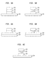
- Figures 6a-6c illustrate a second alternate embodiment.
- silicide layer 232 is anisotropically etched. This layer 232 can then be isotropically etched with an etchant selective to the silicide as shown in Figure 6b. After the undercut is complete, the polysilicon layer 230 can be etched. The resulting structure is shown in Figure 6c, which is similar to that of Figure 4e.
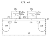
- FIG. 4d The resu1ting structure of each of the embodiments is shown in Figure 4d.
- a pair of wordline stacks are formed by the etching process with a space of less than 5000 Angstroms located between the stacks.
- Each of the stacks are less than about 5000 Angstroms long and include layers 230 and 232.
- the silicon dioxide layer 344 serves as an etch stop. Although only two stacks 230/232 are shown in the figures, it should be understood that a multitude of stacks with spaces located between adjacent stacks can be fabricated using the above described method.
- Sidewall spacer material 252 is then deposited to fill the undercut area completely.
- sidewall spacer 252 is formed by depositing conformal silicon nitride. The requirement for this deposition thickness is half the thickness of the silicide layer 232. In the illustrated example, the undercut region is completely filled along with the region between wordline stacks 230a/232a and 230b/232b.
- the capacitance between the wordline 230/232 and the bitline 240 is reduced because the distance between wordline conductors 232 and bitline contact 242 is increased. In the preferred embodiment, this is accomplished during the formation of the wordlines by performing an undercut in the conductive silicide layer 232. By undercutting the silicide layer 232, a thicker dielectric can be provided between the wordline 232 and the bitline contact 240.
Landscapes
- Engineering & Computer Science (AREA)
- Manufacturing & Machinery (AREA)
- Semiconductor Memories (AREA)
Abstract
Description
Claims (37)
- A transistor device comprising:a first source/drain region disposed in a semiconductor body;a second source/drain region disposed in the semiconductor body, the second source/drain region being spaced from the first source/drain region by a channel region;a dielectric layer overlying the channel region; anda gate electrode overlying the dielectric layer, the gate electrode including:a polysilicon layer extending a first lateral distance over the dielectric layer; anda silicide layer disposed over the polysilicon layer and extending a second lateral distance over the dielectric layer, the second lateral distance being less than the first lateral distance.
- The device of claim 1 wherein the ratio of the first lateral distance to the second lateral distance is about two.
- The device of claim 1 and further comprising a sidewall insulating region disposed along a sidewall of the gate electrode, the sidewall insulating region being thicker at a portion laterally adjacent the silicide layer as compared to a portion laterally adjacent the polysilicon layer.
- The device of claim 3 wherein the portion of the sidewall insulating layer adjacent the silicide layer is thicker than the portion adjacent the polysilicon layer by about half of the difference between the first lateral distance and the second lateral distance.
- A memory device comprising:a first memory cell including:a first source/drain region;a common source/drain region spaced from the first source/drain region by a first channel region;a first gate electrode disposed over the first channel region and insulated therefrom, the first gate electrode including first and second conductors;a first capacitor electrically coupled to the first source/drain region;a second memory cell including:a second source/drain region;the common source/drain region spaced from the second source/drain region by a second channel region;a second gate electrode disposed over the second channel region and insulated therefrom, the second gate electrode including third and fourth conductors;a second capacitor electrically coupled to the second source/drain region;a contact coupled to the common source/drain region and extending upward between the first gate electrode and the second electrode;wherein the distance between the first conductor and the contact is greater than the distance between the second conductor and the contact; andwherein the distance between the third conductor and the contact is greater than the distance between the fourth conductor and the contact.
- The device of claim 5 wherein the first and third conductors each comprise silicide conductors and wherein the second and fourth conductors comprise polysilicon conductors.
- The device of claim 6 wherein first and third conductors each comprise tungsten silicide conductors.
- The device of claim 5 and further comprising a dielectric material disposed between the first and second gate electrodes and the contact.
- The device of claim 5 wherein the distance between the third conductor and the contact is greater than the distance between the fourth conductor and the contact by a factor of at least about two.
- A memory device comprising:a semiconductor body;at least one pair of wordlines disposed over the semiconductor body;a bitline contact disposed between the pair wordlines and a doped region of the semiconductor body; anda bitline coupled to the bitline contact;wherein the wordlines each comprise:a first conductive layer disposed beneath a second conductive layer, the second conductive layer having a width less than the width of said first conductive layer; anda dielectric material disposed on the second conductive layer to separate the second conductive layer from the bitline contact.
- The device of claim 10 wherein the first conductive layer comprises a polysilicon layer and wherein the second conductive layer comprises a metal layer.
- The device of claim 11 wherein the second conductive layer comprises a silicide layer.
- The device of claim 12 wherein second conductive layer comprises a tungsten silicide layer.
- The device of claim 10 wherein the dielectric material has a thickness between about 15 nm and 45 nm between the second conductive layer and the bitline contact.
- A method of forming a transistor device, the method comprising:forming a composite gate layer over a dielectric layer, the composite gate layer including a first conductive layer and a second conductive layer;forming a mask layer over the composite gate layer;patterning and etching the mask layer;patterning and etching the composite gate layer using the mask layer as a mask; andperforming an undercut etch so that a portion of the second conductive layer beneath the mask layer is removed.
- The method of claim 15 wherein the first conductor comprises polysilicon and the second conductor comprises a metal.
- The method of claim 16 wherein the second conductor comprises a silicide.
- The method of claim 17 wherein the second conductor comprises tungsten silicide.
- The method of claim 15 wherein the undercut etch is performed using a reactive ion etch process.
- The method of claim 19 wherein the reactive ion etch process uses a chlorine-oxygen gas chemistry.
- The method of claim 15 wherein forming a mask layer comprises depositing a nitride layer.
- The method of claim 15 wherein the second conductive layer is formed over the first conductive layer, and wherein patterning and etching the composite layer and performing an undercut etch comprise:etching the second conductive layer;etching the first conductive layer using a first etch technique; andcontinuing the first etch technique after a portion of the first conductive layer is removed in order to perform an undercut etch on the second conductive layer.
- The method of claim 15 wherein undercut etch is performed before the first conductive layer of the composite gate layer is etched.
- The method of claim 15 and further'comprising forming source/drain regions adjacent the gate layer subsequent to performing the undercut etch.
- The method of claim 15 wherein the transistor device is formed as part of a dynamic random access memory cell.
- A method for forming a pair of adjacent transistors, the method comprising:etching a conductor having at least two layers into pair of adjacent composite conductors; andlaterally etching a first one of the at least two layers of the conductor at a substantially faster rate than another of the at least two layers to increase lateral separation between a portion of the pair of adjacent composite conductors.
- The method of claim 26 wherein the pair of adjacent composite conductors comprises a pair of wordlines in a DRAM array.
- The method of claim 26 wherein the first one of the two layers comprises a silicide layer and the second one of the two layers comprises a polysilicon layer.
- The method of claim 26 wherein the lateral etching is performed with a reactive ion etch using a chlorine-oxygen etch chemistry.
- A method of decreasing the capacitance between a conductor and an adjacent contact, the method comprising:providing a conductive layer disposed on an upper surface of an semiconductor body;etching the conductive layer in a direction substantial1y perpendicular to the upper surface of the semiconductor body to form adjacent conductors;etching the adjacent conductors laterally thereby increasing the distance between adjacent conductors;forming a dielectric adjacent the adjacent conductors; andforming a contact through the dielectric between the adjacent conductors.
- The method of claim 30 wherein the contact physically contacts with the semiconductor body.
- The method of claim 30 wherein the adjacent conductors comprises wordline conductors of a memory device and wherein the contact comprises a bitline contact.
- The method of claim 30 wherein the conductive is disposed beneath a dielectric layer.
- The method of claim 33 wherein the lateral etching of the adjacent conductors undercuts the dielectric layer.
- The method of claim 30 wherein the conductive layer comprises a composite layer of polysilicon and a silicide.
- The method of claim 30 wherein the etching step comprises a reactive ion etch step.
- The method of claim 36 wherein the reactive ion etch uses a chlorine-oxygen gas mixture.
Applications Claiming Priority (2)
| Application Number | Priority Date | Filing Date | Title |
|---|---|---|---|
| US535445 | 1983-09-23 | ||
| US09/535,445 US6486505B1 (en) | 2000-03-24 | 2000-03-24 | Semiconductor contact and method of forming the same |
Publications (2)
| Publication Number | Publication Date |
|---|---|
| EP1137063A2 true EP1137063A2 (en) | 2001-09-26 |
| EP1137063A3 EP1137063A3 (en) | 2005-04-06 |
Family
ID=24134257
Family Applications (1)
| Application Number | Title | Priority Date | Filing Date |
|---|---|---|---|
| EP01302653A Withdrawn EP1137063A3 (en) | 2000-03-24 | 2001-03-22 | Gate electrode for DRAM transistor |
Country Status (3)
| Country | Link |
|---|---|
| US (1) | US6486505B1 (en) |
| EP (1) | EP1137063A3 (en) |
| TW (1) | TW488037B (en) |
Families Citing this family (7)
| Publication number | Priority date | Publication date | Assignee | Title |
|---|---|---|---|---|
| KR100383325B1 (en) * | 2001-01-19 | 2003-05-12 | 삼성전자주식회사 | Wiring of semiconductor device for forming a self-aligned contact and Method of manufacturing the same |
| US6927462B2 (en) * | 2002-08-28 | 2005-08-09 | Infineon Technologes Richmond, Lp | Method of forming a gate contact in a semiconductor device |
| US7199011B2 (en) * | 2003-07-16 | 2007-04-03 | Texas Instruments Incorporated | Method to reduce transistor gate to source/drain overlap capacitance by incorporation of carbon |
| US20060091478A1 (en) * | 2004-11-04 | 2006-05-04 | Promos Technologies Inc. | Semiconductor gate structure and method for preparing the same |
| US8932210B2 (en) * | 2008-02-28 | 2015-01-13 | K2M, Inc. | Minimally invasive retraction device having detachable blades |
| KR20120137861A (en) * | 2011-06-13 | 2012-12-24 | 삼성전자주식회사 | Non-volatile memory device and mehtod of manufacturing the same |
| US20250234516A1 (en) * | 2024-01-16 | 2025-07-17 | Nanya Technology Corporation | Semiconductor structure including polysilicon as bottom layer of bit line structure and method of manufacturing the same |
Family Cites Families (13)
| Publication number | Priority date | Publication date | Assignee | Title |
|---|---|---|---|---|
| KR950011983B1 (en) * | 1992-11-23 | 1995-10-13 | 삼성전자주식회사 | Fabricating method of semiconductor device |
| KR0141195B1 (en) * | 1994-06-08 | 1998-07-15 | 김광호 | Fabrication method of semiconductor device having low-resistance gate electrod |
| US6060387A (en) * | 1995-11-20 | 2000-05-09 | Compaq Computer Corporation | Transistor fabrication process in which a contact metallization is formed with different silicide thickness over gate interconnect material and transistor source/drain regions |
| US5889331A (en) * | 1996-12-31 | 1999-03-30 | Intel Corporation | Silicide for achieving low sheet resistance on poly-Si and low Si consumption in source/drain |
| US5976930A (en) * | 1997-04-25 | 1999-11-02 | Micron Technology, Inc. | Method for forming gate segments for an integrated circuit |
| US6010954A (en) * | 1997-07-11 | 2000-01-04 | Chartered Semiconductor Manufacturing, Ltd. | Cmos gate architecture for integration of salicide process in sub 0.1 . .muM devices |
| TW365697B (en) * | 1997-11-14 | 1999-08-01 | United Microelectronics Corp | Etching method of improving of self-aligned contact |
| US6153485A (en) * | 1998-11-09 | 2000-11-28 | Chartered Semiconductor Manufacturing Ltd. | Salicide formation on narrow poly lines by pulling back of spacer |
| US6124177A (en) * | 1999-08-13 | 2000-09-26 | Taiwan Semiconductor Manufacturing Company | Method for making deep sub-micron mosfet structures having improved electrical characteristics |
| US6294436B1 (en) * | 1999-08-16 | 2001-09-25 | Infineon Technologies Ag | Method for fabrication of enlarged stacked capacitors using isotropic etching |
| US6218241B1 (en) * | 2000-03-28 | 2001-04-17 | United Microelectronics Corp. | Fabrication method for a compact DRAM cell |
| US6326291B1 (en) * | 2000-06-26 | 2001-12-04 | Advanced Micro Devices, Inc. | Fabrication of a wide metal silicide on a narrow polysilicon gate structure |
| US6406986B1 (en) * | 2000-06-26 | 2002-06-18 | Advanced Micro Devices, Inc. | Fabrication of a wide metal silicide on a narrow polysilicon gate structure |
-
2000
- 2000-03-24 US US09/535,445 patent/US6486505B1/en not_active Expired - Lifetime
-
2001
- 2001-03-22 EP EP01302653A patent/EP1137063A3/en not_active Withdrawn
- 2001-03-23 TW TW090106973A patent/TW488037B/en not_active IP Right Cessation
Also Published As
| Publication number | Publication date |
|---|---|
| US6486505B1 (en) | 2002-11-26 |
| EP1137063A3 (en) | 2005-04-06 |
| TW488037B (en) | 2002-05-21 |
Similar Documents
| Publication | Publication Date | Title |
|---|---|---|
| KR100242352B1 (en) | Method of fabricating a self-aligned contact hole for a semiconductor device | |
| US7888725B2 (en) | Electronic devices including electrode walls with insulating layers thereon | |
| US7279419B2 (en) | Formation of self-aligned contact plugs | |
| US5436188A (en) | Dram cell process having elk horn shaped capacitor | |
| KR100726145B1 (en) | Semiconductor device manufacturing method | |
| KR100261647B1 (en) | Semiconductor device and method of manufacturing the same | |
| US5460999A (en) | Method for making fin-shaped stack capacitors on DRAM chips | |
| US5429980A (en) | Method of forming a stacked capacitor using sidewall spacers and local oxidation | |
| US6218237B1 (en) | Method of forming a capacitor | |
| KR100325472B1 (en) | Manufacturing Method of DRAM Memory Cells | |
| JPH0997880A (en) | Semiconductor memory device and manufacturing method thereof | |
| KR19980086702A (en) | DRAM cell device and manufacturing method thereof | |
| US6479855B1 (en) | Capacitor and conductive line constructions and semiconductor processing methods of forming capacitors and conductive lines | |
| TWI833189B (en) | Semiconductor device and method of fabricating the same | |
| US6806195B1 (en) | Manufacturing method of semiconductor IC device | |
| US5501998A (en) | Method for fabricating dynamic random access memory cells having vertical sidewall stacked storage capacitors | |
| US5807782A (en) | Method of manufacturing a stacked capacitor having a fin-shaped storage electrode on a dynamic random access memory cell | |
| JP3660821B2 (en) | Semiconductor device and manufacturing method thereof | |
| US5536673A (en) | Method for making dynamic random access memory (DRAM) cells having large capacitor electrode plates for increased capacitance | |
| US20010019156A1 (en) | Semiconductor device and fabrication method thereof | |
| US7741682B2 (en) | Semiconductor integrated circuit device including a silicon layer formed on a diffusion layer | |
| US6486505B1 (en) | Semiconductor contact and method of forming the same | |
| US20030054607A1 (en) | Capacitor under bitline (CUB) memory cell structure with reduced parasitic capacitance | |
| US6066541A (en) | Method for fabricating a cylindrical capacitor | |
| US5491104A (en) | Method for fabricating DRAM cells having fin-type stacked storage capacitors |
Legal Events
| Date | Code | Title | Description |
|---|---|---|---|
| PUAI | Public reference made under article 153(3) epc to a published international application that has entered the european phase |
Free format text: ORIGINAL CODE: 0009012 |
|
| AK | Designated contracting states |
Kind code of ref document: A2 Designated state(s): AT BE CH CY DE DK ES FI FR GB GR IE IT LI LU MC NL PT SE TR |
|
| AX | Request for extension of the european patent |
Free format text: AL;LT;LV;MK;RO;SI |
|
| RIN1 | Information on inventor provided before grant (corrected) |
Inventor name: SRINIVASAN, SENTHIL Inventor name: HOH, PETER Inventor name: GAMBINO, JEFFREY P. Inventor name: RUPP, THOMAS S. |
|
| PUAL | Search report despatched |
Free format text: ORIGINAL CODE: 0009013 |
|
| AK | Designated contracting states |
Kind code of ref document: A3 Designated state(s): AT BE CH CY DE DK ES FI FR GB GR IE IT LI LU MC NL PT SE TR |
|
| AX | Request for extension of the european patent |
Extension state: AL LT LV MK RO SI |
|
| RAP1 | Party data changed (applicant data changed or rights of an application transferred) |
Owner name: INTERNATIONAL BUSINESS MACHINES CORPORATION Owner name: INFINEON TECHNOLOGIES AG |
|
| 17P | Request for examination filed |
Effective date: 20050803 |
|
| AKX | Designation fees paid |
Designated state(s): DE FR GB IE IT |
|
| 17Q | First examination report despatched |
Effective date: 20090409 |
|
| STAA | Information on the status of an ep patent application or granted ep patent |
Free format text: STATUS: THE APPLICATION IS DEEMED TO BE WITHDRAWN |
|
| 18D | Application deemed to be withdrawn |
Effective date: 20090820 |