EP1137027A2 - Key panel formed from a strip of printed wiring material and method for making the same - Google Patents
Key panel formed from a strip of printed wiring material and method for making the same Download PDFInfo
- Publication number
- EP1137027A2 EP1137027A2 EP01102258A EP01102258A EP1137027A2 EP 1137027 A2 EP1137027 A2 EP 1137027A2 EP 01102258 A EP01102258 A EP 01102258A EP 01102258 A EP01102258 A EP 01102258A EP 1137027 A2 EP1137027 A2 EP 1137027A2
- Authority
- EP
- European Patent Office
- Prior art keywords
- strip
- key
- printed wiring
- wiring material
- switch
- Prior art date
- Legal status (The legal status is an assumption and is not a legal conclusion. Google has not performed a legal analysis and makes no representation as to the accuracy of the status listed.)
- Withdrawn
Links
Images



Classifications
-
- H—ELECTRICITY
- H01—ELECTRIC ELEMENTS
- H01H—ELECTRIC SWITCHES; RELAYS; SELECTORS; EMERGENCY PROTECTIVE DEVICES
- H01H13/00—Switches having rectilinearly-movable operating part or parts adapted for pushing or pulling in one direction only, e.g. push-button switch
- H01H13/70—Switches having rectilinearly-movable operating part or parts adapted for pushing or pulling in one direction only, e.g. push-button switch having a plurality of operating members associated with different sets of contacts, e.g. keyboard
- H01H13/702—Switches having rectilinearly-movable operating part or parts adapted for pushing or pulling in one direction only, e.g. push-button switch having a plurality of operating members associated with different sets of contacts, e.g. keyboard with contacts carried by or formed from layers in a multilayer structure, e.g. membrane switches
-
- H—ELECTRICITY
- H01—ELECTRIC ELEMENTS
- H01H—ELECTRIC SWITCHES; RELAYS; SELECTORS; EMERGENCY PROTECTIVE DEVICES
- H01H2229/00—Manufacturing
- H01H2229/022—Modular assembly
-
- H—ELECTRICITY
- H01—ELECTRIC ELEMENTS
- H01H—ELECTRIC SWITCHES; RELAYS; SELECTORS; EMERGENCY PROTECTIVE DEVICES
- H01H2229/00—Manufacturing
- H01H2229/034—Positioning of layers
-
- H—ELECTRICITY
- H01—ELECTRIC ELEMENTS
- H01H—ELECTRIC SWITCHES; RELAYS; SELECTORS; EMERGENCY PROTECTIVE DEVICES
- H01H2229/00—Manufacturing
- H01H2229/038—Folding of flexible printed circuit
Definitions
- the present invention relates to key panels in general and more specifically to a key panel formed from a single strip of switch material and a method for making the key panel.
- Key panels or keyboards have been used for decades to provide input and control instructions to electronic devices and systems.
- Early key panel systems were discrete systems, typically comprising an array of individual mechanical switches arranged and mounted so as to form the desired key panel configuration.
- early QWERTY (e.g., typewriter-style) key panel systems were constructed according to this architecture.
- Such discrete type key panel or keyboard systems are expensive and difficult to produce.
- membrane type key panel systems In which the various switches are provided on thin, flexible substrates or membranes. Such key panel systems are often generically referred to as membrane type key panel systems. While many different types of membrane type key panel systems exist and are being used, a typical membrane type key panel system comprises a laminated or layered structure in which a bottom membrane layer or sheet is provided with a plurality of switch elements that correspond to each desired input key. An overlying flexible layer or membrane may be provided with one or more raised portions or "domes" thereon that are aligned with the switch contacts provided on the bottom layer or membrane. Each switch on the bottom membrane may be actuated by depressing the corresponding dome on the overlying or top layer.
- Membrane type key panels of the type just described have become very popular and are widely used in modern electronic devices and systems due to their reliable operation, light weight, and rugged construction.
- membrane type key panel systems are not readily adaptable to varying panel or keyboard configurations.
- a currently available membrane type key system is produced as a two dimensional sheet or panel having a size and shape that corresponds to the specific key panel layout for the particular device in which the key panel is to be used. Therefore, if the key panel layout is changed, an entirely new sheet or panel of the switch membrane material must be produced that corresponds to the changed key panel layout.
- a user desires to utilize a key panel configuration wherein the keys are placed around the periphery of the panel, such as for example, if the keys are to be placed around a centrally located two dimensional display device (e.g., a CRT or and LCD display), the sheet material located in the corresponding central region of the key panel will need to be removed, thus wasted, in order to accommodate the display device. Such waste increases the overall cost of the key panel device.
- a disadvantage associated with currently available membrane type key panel systems is that two dimensional sheets or panels are difficult to ship and store, particularly if the key panel in which they are to be used is relatively large.
- a key panel comprises a key pad having a number of key sites provided thereon that define an aspect ratio for the key pad.
- a strip of printed wiring material is positioned adjacent the key pad.
- a number of switch contact sites provided on the strip of printed wiring material define an aspect ratio for the strip of printed wiring material that is greater than the aspect ratio of the key pad.
- the strip of printed wiring material is provided with at least one fold therein so that each of the number of switch contact sites provided on the strip of printed wiring material is generally aligned with a corresponding one of the number of key sites provided on the key pad.
- Also disclosed is a method for fabricating a key panel that comprises the steps of: Selecting a key pad having a number of key sites provided thereon which define an aspect ratio for the key pad; selecting a strip of printed wiring material having a number of switch contact sites thereon that define an aspect ratio that is greater than the aspect ratio of the key pad; and folding the strip of printed wiring material so as to align ones of the number of switch contact sites with corresponding ones of the number of key sites.
- a key panel assembly 10 is best seen in Figure 1 and may comprise a strip of switch material 12 folded so that it conforms to a desired key panel configuration 14.
- the key panel configuration 14 is not necessarily a physical element but instead represents a desired configuration for the key locations for a desired device (not shown), such as a portable or hand-held scanner device.
- the key panel configuration 14 may comprise a generally rectangular shape having a number of switch locations 16 arranged in a generally U-shaped pattern 18. The arrangement of the switch locations 16 in the pattern 28 defines an aspect ratio for the key panel configuration 14.
- the aspect ratio for the key panel configuration 14 is defined as the ratio of the overall length 20 between the switch locations 16 that are separated by the greatest distance along the length direction and the overall width 22 between the switch locations that are separated by the greatest distance along the width direction.
- the aspect ratio is the overall length 20 divided by the overall width 22.
- the strip of switch material 12 may comprise an elongate, generally flexible member having a front side 21 and a back side 23.
- One or more switches 24 are provided on the strip of switch material 12.
- the switches 24 on the strip of switch material 12 define an aspect ratio for the strip of switch material 12.
- the aspect ratio for the strip of switch material 12 is defined as the ratio of the overall length 26 between the switches 24 that are located at either end of the strip of switch material 12 and the overall width 28 between the switches 24 that are separated by the greatest distance along the width direction.
- the aspect ratio of the strip of switch material 12 is the overall length 26 divided by the overall width 28.
- the key panel assembly 10 is formed by selecting a strip of switch material 12 having a numerical aspect ratio (i.e., the overall length 26 of the strip of switch material 12 divided by overall width 28 of the strip of switch material) that is greater than the numerical aspect ratio (i.e., overall length 20 of the key panel configuration 14 divided by overall width 22 of the key panel configuration 14) of the key panel configuration 14.
- the strip of switch material 12 should also contain at least as many switches 24 as their are switch locations 16 in the key panel configuration 14.
- the strip of switch material 12 is then provided with one or more folds 30 so as to arrange the various switches 24 provided on the strip of switch material 12 in accordance with the pattern 18 defined by the key panel configuration 14.
- the strip of switch material 12 is folded so that each switch 24 is positioned at the corresponding switch location 16 provided on the key panel configuration 14. See Figure 1.
- the strip of switch material 12 may then be incorporated into the device (not shown) in which the key panel assembly 10 is to be used.
- the folded and configured strip of switch material 12 may be affixed to a subpanel 42 ( Figure 4) associated with the device (not shown) and covered with a control panel bezel 32 ( Figure 1).
- a significant advantage of the key panel assembly 10 according to the present invention is that it allows the key panel 10 to be formed with a single, continuous strip of switch material 12, thereby eliminating much of the waste typically associated with prior key panels formed from two-dimensional sheets of key switch material (not shown).
- a key panel fabricated from a two-dimensional sheet (not shown) about the same size as the rectangular key panel configuration 14 would include a large waste area roughly corresponding to an area 34 on the key panel configuration 14 that is devoid of switches. That is, the waste area on the two-dimensional sheet of key panel material would be about the same size as a display window 36 provided on the bezel assembly 32.
- the present invention eliminates such waste in that the strip of switch material need not be positioned in the waste area 34.
- Another advantage of the present invention is that it allows key panels having almost any size and shape (i.e., key panel configuration) to be manufactured from a single, continuous strip of switch material 12 by simply folding and bending the strip of switch material 12 as necessary to form the desired configuration. Accordingly, the present invention also eliminates the need to provide separate, and typically custom-designed, two-dimensional key panel sheets for a given product or product line. The present invention thus represents a paradigm shift: It allows membrane type key panels to be fabricated from a single strip of switch material as opposed to using a larger two-dimensional sheet or panel of membrane type switch material.
- the flexible nature of the strip of switch material 12 allows the material to be used to form three-dimensional key panel configurations, i.e., configurations wherein switches may be located on a front surface, a side surface, and a back surface of the device.
- the strip of switch material 12 may also be used with curved key panel configurations in which a given surface of the key panel may be curved in three dimensions.
- the various embodiments of the key panel according to present invention will now be described in detail. However, before proceeding with the detailed description, it should be noted that only a limited number of configurations and examples for the key panel are shown and described herein. Many other configurations are possible and may be used in any of a wide variety of applications. Indeed, the key panel assembly according to the present invention may be used in almost any configuration and for any device imaginable, be it a currently existing device, or some device yet to be developed. Consequently, the present invention should not be regarded as limited to the particular configurations, applications, and devices shown and described herein.
- FIGs 1-4 one embodiment of the key panel assembly 10 according to the present invention is best seen in Figures 1-4 as it may be used to form the key panel associated with a portable or hand-held scanner device (not shown).
- the bezel assembly 32 of such a portable or hand-held scanner device is shown in Figure 1.
- the functional and/or aesthetic requirements of the particular device in which the key panel assembly 10 is to be used will lead a designer to develop a key panel configuration 14 which defines a variety of switch locations 16 arranged in a pattern 18.
- the exact number of switch locations 16 and the particular pattern 18 in which they are arranged will vary from device to device.
- a designer will be able to utilize the strip of switch material 12 in almost any key panel configuration 14 that can be imagined.
- the key panel configuration 14 may comprise a plurality of switch locations 16 arranged in a generally U-shaped pattern 18. It should be noted that the key panel configuration is not necessarily a physical device or structure and could instead simply comprise a plan or construct used to guide the development of the device and to define the locations of the various switches to be contained in the key panel. Consequently, the present invention should not be regarded as limited to a physical key panel configuration 14.
- the key panel configuration 14 may also be provided with a multi-switch location 16' which may comprise four individual switch locations 16" arranged in a group to define the multi-switch location 16'. Such multi-switch locations 16' may be accommodated by the present invention by providing the strip of switch material 12 with a corresponding grouping 24' of individual switches 24", as discussed below. Alternatively, such multi-switch locations 16' need not be provided.
- the pattern 18 of switch locations 16 defining the key panel configuration 14 also define an aspect ratio for the key panel configuration 14.
- the aspect ratio of the key panel configuration 14 is the ratio of the overall length 20 to the overall width 22 of the switch locations 16 defining the key panel configuration.
- the aspect ratio of the key panel configuration 14 is the overall length 20 of the key panel configuration 14 divided by the overall width 22 of the key panel configuration 14.
- the overall length 20 is defined as the length between the center lines of the two switch locations 16 that are separated by the greatest distance in the length direction.
- the overall length 20 of the key panel configuration 14 is the distance separating the center line of the left-most small switch location 16" in the multi-switch location 16' and the center line of any of the right-most switch locations 16, since those switch locations 16 are all substantially co-linear.
- the overall width 22 of the key panel configuration 14 is defined as the length between the center lines of the two switch locations 16 that are separated by the greatest distance in the width direction.
- the overall width 22 of the key panel configuration 12 is the distance separating the center lines of any of the lower-most switch locations 16, since they are all substantially co-linear, and the center lines of either of the upper-most switch locations 16, since they are also substantially co-linear.
- the strip of switch material 12 is best seen in Figure 3 and may comprise an elongate, generally flexible member having a front side 21 and a back side 23.
- the strip of switch material 12 may also be provided with a plurality of switches 24 which are operable from the front side 21 of the strip of switch material 12.
- each switch 24 provided on the strip of switch material 12 may be substantially identical to the others and may be located at substantially evenly spaced locations along the length of the strip of switch material 12. However, other configurations are possible.
- the strip of switch material 12 may be provided with a corresponding grouping 24' of individual switches 24", as best seen in Figures 1 and 3.
- the arrangement of switches (e.g., 24, 24") on the strip of switch material 12 defines an aspect ratio for the strip of switch material 12.
- the aspect ratio of the strip of switch material 12 is the ratio of the overall length 26 to the overall width 28.
- the aspect ratio of the strip of switch material 12 is the overall length 26 divided by the overall width 28.
- the overall length 26 is defined as the distance separating the center lines of the two switches 24 that are located the greatest distance apart along the length direction, i.e., the distance between center lines of the two switches 24 that are located at opposite ends of the strip of switch material 12.
- the overall length 26 of the strip of switch material 12 is defined as that distance separating the center line of the left-most switch 24 and the center line of the right-most switch 24.
- the overall width 28 of the strip of switch material 12 is the distance separating the center lines of the two switches 24 that are located the greatest distance apart in the width direction.
- the overall width 28 is the distance between the center line of the upper-most switch 24" and the center line of the lower-most switch 24" contained in the group of switches 24'.
- the strip of switch material 12 comprises a single, substantially co-linear row of switches 24, then the width dimension 28 should be regarded as unity in order to avoid an indefinite aspect ratio when expressed arithmetically.
- the relationship between the aspect ratios of the key panel configuration 14 and the strip of switch material 12 provides a convenient method for defining a part of the invention. That is, if the aspect ratio (expressed arithmetically) of the strip of switch material 12 is greater than the aspect ratio (expressed arithmetically) of the key panel configuration 14, then the strip of switch material 12 may be regarded as being used in accordance with the teachings of the present invention. Stated another way, the strip of switch material 12 may be regarded as a one-dimensional array of switches 24.
- the use of the strip of switch material 12 in a key panel configuration 14 having a lower aspect ratio essentially amounts to a use of the one-dimensional array of switches 24 contained in the strip of switch material 12 to form a two-dimensional array of switches in the desired key panel assembly 10.
- the aspect ratio measure is used to cover a situation, such as that illustrated in Figures 1-3, where one or more switch locations 16 in the key panel configuration 14 may comprise a group 16' of multiple switch locations 16". Absent the aspect ratio definitions provided herein, a strip of switch material 12 having a corresponding group 24' of switches 24" would not be properly regarded as a strictly one-dimensional array of switches.
- the strip of switch material 12 should include at least as many switches 24 as there are switch locations 16 in the key panel configuration 14. If the strip of switch material 12 contains switches 24 in excess of the number of switch locations 16, such additional switches 24 will simply remain unused in the final key panel assembly 10. Referring back now to Figure 1, the strip of switch material 12 may be provided with one or more folds 30 in order to arrange the various switches 24, 24" provided on the strip of switch material 12 so that the switches 24, 24" may be arranged to conform to the switch pattern 18 defined by the key panel configuration 14.
- the strip of switch material 12 may be configured to conform to the key panel configuration 14 by first folding the vertical portion 37 of the strip of switch material 12 upwardly and then by folding it outwardly.
- the two folds 30 serve to reconfigure the switches 24 on the strip 12 so that they extend along a substantially horizontal portion 38.
- the strip of switch material 12 is then folded twice again so as to reconfigure the remaining switches 24 on the strip 12 so that they extend along a substantially vertical portion 40.
- the strip of switch material 12 may then be secured to a subpanel 42 ( Figure 4), if desired, and connected to the electrical circuitry (not shown) associated with the device (also not shown).
- An optional bezel 32 ( Figure 1) may then be secured over the key panel assembly 10, as-will be discussed in greater detail below.
- each fold 30 should be greater than or equal to the minimum bend radius associated with the particular type of switch material that is used to form the strip of switch material 12. So limiting the minimum radius of the various folds 30 will ensure reliable and long-lived operation of the key panel assembly 10. Since the minimum bend radius of the switch material 12 will vary depending on the particular configuration and structural attributes of the switch material, as described in greater detail below, the present invention should not be regarded as limited to materials having any particular minimum bend radius.
- the strip of switch material 12 may comprise any of a wide range of flexible, membrane-type switch devices that are well-known in the art and that are readily commercially available.
- the strip of switch material 12 may comprise a flexible membrane switch assembly available from GM Nameplate, Intaq Electrotouch Systems, of Seattle, WA.
- similar membrane type switches are available from Shin-Etsu Polymer of Union City, CA.
- One configuration of such a membrane type switch will now be described in order to provide a better framework for understanding the invention.
- one embodiment of the strip of switch material 12 may comprise a generally flexible, membrane type switch material comprising a generally flexible bottom membrane 44 having at least one switch contact 46 formed thereon. While a wide variety of switch contacts 46 are known for such devices, in one preferred embodiment switch contact 46 may be formed from first and second conductive elements 48 and 50 deposited on the bottom membrane 44. The first and second conductive elements 48 and 50 may be electrically connected together to close the switch. A top membrane 52 having at least one dome 54 formed thereon may be positioned over the switch contact 46 so that an electrically conductive portion 56 of dome 54 will electrically connect together at least portions of the first and second conductive elements 48 and 50 when the dome 54 is depressed.
- the foregoing switch structure is generically referred to in the art as a "membrane switch," although other terms are also used to describe this structure.
- the top membrane 52 may be separated from the bottom membrane 44 by a spacer 58.
- Spacer 58 defines an opening 60 therein that is aligned with the switch contact 46 and the dome 54.
- an overlay member 62 may be positioned over the top membrane 52 to protect the same from wear, foreign objects, and/or liquids. Overlay member 62 may be separated from the top membrane 52 by a spacer member 64.
- the lower membrane 44 may be positioned adjacent a subpanel member 42 which provides support for the strip of switch material 12. If necessary or desired in any particular application, the lower membrane 44 may be affixed to the subpanel member 42 by any of a wide range of adhesive materials that are readily commercially available for such purposes.
- a second embodiment 110 of the key panel assembly illustrated in Figure 1 may be provided with a strip of switch material 112 having a plurality of additional folds 131 provided therein in order to position the switches 124 provided therein so that the switches 124 that are to be used are all substantially co-planar.
- the folds 131 are in addition to folds 130 which may be used to align the various switches.124 in the pattern (e.g., the pattern 18 shown in Figure 1) defined by the particular key panel configuration (e.g., the key panel configuration 14 shown in Figure 1).
- each fold 130, 131 should have a radius (not shown) equal to or greater than the minimum bend radius associated with the particular switch material used.
- a third embodiment 210 of a key pad assembly may comprise a strip of switch material 212 folded so that at least one switch 224 is located on the front side 221 of the strip of switch material 212 and so that at least one switch 224' is located on the back side 223 of the strip of switch material 212.
- this configuration may be obtained by providing the strip of switch material 212 with two folds 230 as shown.
- the strip of switch material may comprise any of a wide range of flexible materials having switches provided thereon that may be folded in accordance with the present invention in order to form the key panel assembly (e.g., 10, 110, 210) of the present invention.
- a key panel assembly is shown in Figure 7 and may comprise a strip of switch material 312 comprising a generally flexible bottom membrane 344 having at least one switch contact 346 provided thereon.
- Switch contact 346 may comprise first and second conductive elements 348 and 350 positioned in spaced-apart relation on the bottom membrane 344.
- a top membrane 352 having a dome 354 provided thereon may be positioned over the bottom membrane 344.
- the dome 354 may be provided with an electrically conductive region 356 thereon so that when dome 354 is depressed, the electrically conductive region 356 will electrically connect at least portions of the first and second conductive elements 348 and 350, thus closing the switch 324.
- the key panel assembly 310 may be provided with a key top 366 positioned over the dome 354.
- a bezel 332 defining an opening 333 therein may also be provided to hold key top 366 in position.
- the bottom membrane 344 may be positioned adjacent a subpanel 342 which provides support for the strip of switch material 312.
- the bottom membrane 344 may be attached to the subpanel 342 by any suitable adhesive material.
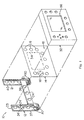
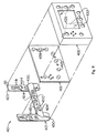
- FIG. 8 and 9 Another embodiment 410 of a key panel assembly according to the present invention is illustrated in Figures 8 and 9.
- the embodiment 410 of the key panel assembly is similar to the previous embodiments already described, except that the embodiment 410 utilizes a strip of printed wiring material 412 and a key pad 413 instead of the strip of switch material (e.g., 12).
- the strip of printed wiring material 412 is provided with a number of switch contact sites 424 thereon which may be activated (e.g., closed) by pushing on corresponding key sites 425 provided on the key pad 413.
- each key site 425 is provided with an electrically conductive portion 456 ( Figure 9) thereon which electrically connects first and second conductive elements 448 and 450 which form the switch contact sites 424 on the strip of printed wiring material 412.
- the strip of printed wiring material 412 is easier and less-expensive to fabricate than is the strip of switch material (e.g., 12).
- the strip of printed wiring material 412 need not comprise a complex, laminated structure having a spacer (e.g., 58) and a top membrane (e.g., 52) having one or more domes (e.g., 54) provided thereon.
- the simpler structure of the strip of printed wiring material 412 allows its configuration (i.e., the locations of the switch contact sites 424) to be easily changed during fabrication, thereby allowing for the production of strips of printed wiring material having different configurations for different key panel layouts.
- the strip of printed wiring material 412 may be fabricated by any of a wide variety of so-called “continuous” (as opposed to batch) production techniques that are well-known in the art for producing printed wiring material. Many such continuous production techniques also allow the configuration (i.e., the locations of the switch contact sites 424) to be changed "on-the-fly.”
- the strip of printed wiring material 412 embodiment 410 of the key panel assembly may comprise an elongate, generally flexible substrate 444 having a front side 421 and a back side 423.
- the strip of printed wiring material 412 may also be provided with a plurality of switch contact sites 424 thereon which are operable from the front side 421 of the strip of printed wiring material 412.
- the strip of printed wiring material 412 may also be provided with switch contact sites (not shown) that are operable from the back side 423 of the strip of printed wiring material 412.
- each of the switch contact sites 424 may be formed from first and second conductive elements 448 and 450 deposited on the substrate 444.
- the first and second conductive elements 448 and 450 may be electrically connected together to close the switch.
- the back side 427 of each key site 425 provided on the key pad 413 may be provided with an electrically conductive portion 456 which electrically connects together the first and second conductive elements 448 and 450 when the key site 425 is depressed.
- the strip of printed wiring material 412 may be fabricated from any of a wide range of materials and in accordance with any of a wide range of techniques that are well-known in the art for fabricating flexible printed wiring material. Consequently, the present invention should not be regarded as limited to printed wiring materials fabricated with any particular type of material or in accordance with any particular process.
- the membrane 444 may be fabricated from any of a wide variety of materials, such as, for example, polyimide films, polyester films, aramid papers, reinforced composite materials, or fluorocarbon materials.
- the electrically conductive elements 448 and 450 contained on the strip of printed wiring material 412 may comprise any of a wide range of materials that are also well-known in the art and suitable for such purposes, including, without limitation, copper, beryllium copper, aluminum, and polymer thick film (PTF) conductors.
- the strip of printed wiring material 412 may also be coated with a suitable protective coating or cover layer (not shown) having apertures (also not shown) formed therein to expose the switch contact sites 424.
- cover layers include, but are not limited to, polyester, polyimide, fluorocarbon films, aramid papers, and epoxies.
- the arrangement of the switch contact sites 424 on the strip of printed wiring material 412 defines an aspect ratio for the strip of printed wiring material 412.
- the aspect ratio of the strip of printed wiring material 412 is the ratio of the overall length (not shown in Figures 8 and 9, but indicated generally as length 26 in Figure 3 for the strip of switch material 12) to the overall width (not shown in Figures 8 and 9, but shown as width 28 in Figure 3 for the strip of switch material 12).
- the overall length is defined as the distance separating two switch contact sites 424 that are located the greatest distance apart along the length direction.
- the overall width of the strip of printed wiring material 412 is the distance separating two switch contact sites 424 that are located the greatest distance apart in the width direction.
- the key pad 413 is best seen in Figure 8 and may comprise a flexible, generally sheet-like member having one or more key sites 425 formed thereon.
- the key sites 425 are arranged in a generally U-shaped pattern.
- the back side 427 of each key site 425 may be provided with an electrically conductive portion or element 456 ( Figure 9) suitable for electrically connecting together the first and second conductive elements 448 and 450 comprising the switch contact sites 424 contained on the strip of printed wiring material 412 when the key site 425 is depressed.
- the pattern of key sites 425 on the key pad 413 define an aspect ratio for the key pad 413.
- the aspect ratio of the key pad 413 is the ratio of the overall length (not shown in Figure 8, but indicated generally as length 20 in Figure 2 for the key panel configuration 14) to the overall width (not shown in Figure 8, but shown as width 22 in Figure 2 for the key panel configuration 14).
- the overall length is defined as the length between two key sites 425 that are separated by the greatest distance in the length direction.
- the overall width is defined as the length between two key sites 425 that are separated by the greatest distance in the width direction.
- the key pad 413 may be fabricated from any of a wide range of materials now known in the art or that may be developed in the future that would be suitable for the intended application.
- the key pad 413 is molded as a single, unitary piece from a silicone rubber material of the type commonly used to fabricate such key pads.
- the electrically conductive element 456 provided on the back side 427 of each key site 425 may comprise a carbon disk or "pellet" which may then be affixed to the back side 427 of key site 425 by any suitable means (e.g., adhesives).
- the electrically conductive element 456 may be comprise an integral, electrically conductive portion of the key pad 413.
- the strip of printed wiring material 412 may be provided with one or more folds 430 ( Figure 8) therein in order to arrange the various switch contact sites 424 so that they are generally aligned with the key sites 425 provided in the key pad 413.
- the radius (not shown) of each fold 430 be greater than or equal to the minimum bend radius associated with the particular type of printed wiring material that is used to form the strip of printed wiring material 412. So limiting the minimum radius of the various folds 430 ensures reliable and long-lived operation of the key panel assembly 410. Since the minimum bend radius of the strip of printed wiring material 412 will vary depending on the particular configuration and structural attributes of the printed wiring material, the present invention should not be regarded as limited to materials having any particular minimum bend radius.
- the strip of printed wiring material 412 be secured to a sub-panel 442 ( Figure 9) to provide additional structural support for the strip of printed wiring material 412.
- An optional bezel 432 ( Figure 8) having a plurality of openings 433 therein that are generally aligned with the key sites 425 provided on the key pad 413 may be secured over the key panel assembly 410, as best seen in Figure 8.
- the bezel 432 with a plurality of alignment pins 435 that are sized to engage corresponding holes 439 and 441 provided in the key pad 413 and strip of printed wiring material 412, respectively.
- the alignment pins 435 improve the alignment accuracy of the key panel assembly 410, ensuring that each key site 425 provided on the key pad 413 is properly aligned with its corresponding contact site 424 on the strip of printed wiring material 412.
- the alignment pins 435 also simplify assembly. If a sub-panel 442 is provided, sub-panel 442 may be provided with corresponding blind or through holes 443 ( Figure 9) suitable for receiving the alignment pins 435 provided on bezel 432.
Landscapes
- Push-Button Switches (AREA)
- Input From Keyboards Or The Like (AREA)
- Manufacture Of Switches (AREA)
Abstract
Description
Claims (10)
- A key panel (410), comprising:a key pad (413) having a number of key sites (425) provided thereon that define an aspect ratio for said key pad (413); anda strip of printed wiring material (412) positioned adjacent said key pad (413), said strip of printed wiring material (412) having a number of switch contact sites (424) provided thereon that define an aspect ratio for said strip of printed wiring material (412) that is greater than the aspect ratio of said key pad (413), said strip of printed wiring material (412) having at least one fold (430) formed therein so that each of the number of switch contact sites (424) provided on said strip of printed wiring material (412) is generally aligned with a corresponding one of the number of key sites (425) provided on said key pad (413).
- The key panel (410) of claim 1, wherein said strip of printed wiring material (412) comprises:a substrate (444); andan electrical conductor adhered to said substrate (444), said electrical conductor forming the number of switch contact sites (424).
- The key panel (410) of claims 1 or 2, wherein each of the number of switch contact sites (424) formed by said electrical conductor comprises a first electrically conductive trace (448) and a second electrically conductive trace (450), said first and second electrically conductive traces (448, 450) being positioned in spaced-apart relationship on said substrate (444), and wherein each of the number of key sites (425) provided on said key pad (413) comprises an electrically conductive portion (456), the electrically conductive portion (456) on each of the number of key sites (425) contacting at least portions of both said first and second electrically conductive traces (448, 450) on said substrate (444) when each of the number of key sites (425) is depressed.
- The key panel (410) of claims 1, 2, or 3, further comprising a bezel (432) defining a number of openings (433) therein aligned with the number of key sites (425) provided on said key pad (413), said bezel (432) being positioned over said key pad (413) so that the number of key sites (425) may be accessed by an operator through the number of openings (433) provided in said bezel (432).
- The key panel (410) of claims 1, 2, 3, or 4, further comprising at least one alignment pin (435) provided on said bezel (432), and wherein said key pad (413) defines at least one through hole (439) therein sized to receive said at least one alignment pin (435) on said bezel (432) and wherein said strip of printed wiring material (412) defines at least one through hole (441) therein sized to receive said at least one alignment pin (435) on said bezel (432), said at least one alignment pin (435) of said bezel (432) aligning the key sites (425) provided on said key pad (413) with corresponding ones of the switch contact sites (424) provided on said strip of printed wiring material (412).
- The key panel (410) of claims 1, 2, 3, 4, or 5, wherein said strip of printed wiring material (412) comprises a front side (421) and a back side (423), each of said switch contact sites (424) provided in said strip of printed wiring material (412) being actuated from the front side (421) of said strip of printed wiring material (412).
- The key panel (410) of claims 1, 2, 3, 4, 5, or 6, wherein said strip of printed wiring material (412) comprises a front side (421) and a back side (423), wherein at least one of the number of switch contact sites (424) is provided on the front side (421) of said strip of printed wiring material (412) and wherein at least one of the number of switch contact sites (424) is provided on the back side (423) of said strip of printed wiring material (412).
- The key panel (410) of claims 1, 2, 3, 4, 5, or 6, wherein said key pad (413) is positioned adjacent the front side (421) of said strip of printed wiring material (412) and further comprising a second key pad positioned adjacent the back side (423) of said strip of printed wiring material (412).
- A key panel (410), comprising:a key pad (413) having a number of key sites (425) arranged in a pattern so as to define an aspect ratio for said key pad (413); anda strip of printed wiring material (412) having a number of switch contact sites (424) provided thereon so as to define an aspect ratio for said strip of printed wiring material (412) that is greater than the aspect ratio of said key pad (413), said strip of printed wiring material (412) having at least one fold (430) formed therein so as to arrange in the pattern the number of switch contact sites (424) provided on said strip of printed wiring material (412).
- A method for fabricating a key panel (410), comprising:selecting a key pad (413) having a number of key sites (425) provided thereon that define an aspect ratio for said key pad (413);selecting a strip of printed wiring material (412) having a number of switch contact sites (424) provided thereon that define an aspect ratio for said strip of printed wiring material (412) that is greater than the aspect ratio of said key pad (413); andfolding said strip of printed wiring material (412) so as to align ones of the number of switch contact sites (424) with corresponding ones of the number of key sites (425).
Applications Claiming Priority (4)
| Application Number | Priority Date | Filing Date | Title |
|---|---|---|---|
| US09/514,213 US6365848B1 (en) | 2000-02-25 | 2000-02-25 | Key panel and strip switch assembly configurations having variable aspect ratios and method of making |
| US514213 | 2000-02-25 | ||
| US09/612,550 US6359242B1 (en) | 2000-02-25 | 2000-07-07 | Key panel including key pad and strip of printed wiring material having various aspect ratios and method of making |
| US612550 | 2000-07-07 |
Publications (2)
| Publication Number | Publication Date |
|---|---|
| EP1137027A2 true EP1137027A2 (en) | 2001-09-26 |
| EP1137027A3 EP1137027A3 (en) | 2003-06-25 |
Family
ID=27058141
Family Applications (1)
| Application Number | Title | Priority Date | Filing Date |
|---|---|---|---|
| EP01102258A Withdrawn EP1137027A3 (en) | 2000-02-25 | 2001-01-31 | Key panel formed from a strip of printed wiring material and method for making the same |
Country Status (2)
| Country | Link |
|---|---|
| EP (1) | EP1137027A3 (en) |
| JP (1) | JP2001291452A (en) |
Families Citing this family (1)
| Publication number | Priority date | Publication date | Assignee | Title |
|---|---|---|---|---|
| FR2860914B1 (en) * | 2003-10-14 | 2006-04-14 | Bosch Rexroth Dsi Sas | CONTROL HANDLE FOR MANIPULATOR |
Family Cites Families (2)
| Publication number | Priority date | Publication date | Assignee | Title |
|---|---|---|---|---|
| US4417105A (en) * | 1981-10-26 | 1983-11-22 | W. H. Brady Co. | Membrane switch assembly with modular switch portions |
| US4681987A (en) * | 1983-01-11 | 1987-07-21 | Canon Kabushiki Kaisha | Electronic equipment having a key input function |
-
2001
- 2001-01-31 EP EP01102258A patent/EP1137027A3/en not_active Withdrawn
- 2001-02-23 JP JP2001047765A patent/JP2001291452A/en active Pending
Also Published As
| Publication number | Publication date |
|---|---|
| EP1137027A3 (en) | 2003-06-25 |
| JP2001291452A (en) | 2001-10-19 |
Similar Documents
| Publication | Publication Date | Title |
|---|---|---|
| US6359242B1 (en) | Key panel including key pad and strip of printed wiring material having various aspect ratios and method of making | |
| US4818827A (en) | Low force membrane switch | |
| US4028509A (en) | Simplified tabulator keyboard assembly for use in watch/calculator having transparent foldable flexible printed circuit board with contacts and actuator indicia | |
| US5748114A (en) | Flat input keyboard for data processing machines or the like and process for producing the same | |
| US4499343A (en) | Monolithic flat tactile keyboard | |
| DE60108868T2 (en) | INPUT DEVICES AND THEIR USE | |
| US4317011A (en) | Membrane touch switch | |
| GB2133218A (en) | Membrane keyboard electrical switch | |
| EP2593311B1 (en) | Electronic device and a method of manufacturing such a device. | |
| JPH0784693A (en) | Interactive braille device | |
| EP0365787A2 (en) | Capacitance membrane switchcore with intertrace capacitive coupling and/or intratrace capacitive coupling | |
| US4218600A (en) | Connecting flexible switch | |
| CA1106428A (en) | Control panel overlay | |
| CN102262480B (en) | Touch panel and method of manufacturing the same | |
| US5220598A (en) | Telephone | |
| GB2109635A (en) | A flexible membrane electric switch | |
| US4736190A (en) | Sheet membrane keyboard and electronic apparatus using same | |
| US4217473A (en) | Connecting flexible switch | |
| EP1211590B1 (en) | Double-sided keyboard having a spacer plate with apertures to hold contacts | |
| EP1137027A2 (en) | Key panel formed from a strip of printed wiring material and method for making the same | |
| EP2668833B1 (en) | Electronic component | |
| US4510353A (en) | Method and kit for construction of custom prototype membrane switch panel | |
| US20120133593A1 (en) | Digitizer for a fingertip tactile-sense input device | |
| JPH05204528A (en) | Digitizer screen and manufacture thereof | |
| US6483051B2 (en) | Method in the manufacture of a keyboard for an electronic device |
Legal Events
| Date | Code | Title | Description |
|---|---|---|---|
| PUAI | Public reference made under article 153(3) epc to a published international application that has entered the european phase |
Free format text: ORIGINAL CODE: 0009012 |
|
| AK | Designated contracting states |
Kind code of ref document: A2 Designated state(s): AT BE CH CY DE DK ES FI FR GB GR IE IT LI LU MC NL PT SE TR |
|
| AX | Request for extension of the european patent |
Free format text: AL;LT;LV;MK;RO;SI |
|
| PUAL | Search report despatched |
Free format text: ORIGINAL CODE: 0009013 |
|
| AK | Designated contracting states |
Designated state(s): AT BE CH CY DE DK ES FI FR GB GR IE IT LI LU MC NL PT SE TR |
|
| AX | Request for extension of the european patent |
Extension state: AL LT LV MK RO SI |
|
| 17P | Request for examination filed |
Effective date: 20030731 |
|
| AKX | Designation fees paid |
Designated state(s): DE FR GB |
|
| GRAP | Despatch of communication of intention to grant a patent |
Free format text: ORIGINAL CODE: EPIDOSNIGR1 |
|
| STAA | Information on the status of an ep patent application or granted ep patent |
Free format text: STATUS: THE APPLICATION IS DEEMED TO BE WITHDRAWN |
|
| 18D | Application deemed to be withdrawn |
Effective date: 20060703 |