EP1136269A2 - Ink jet head having a plurality of units and its manufacturing method - Google Patents
Ink jet head having a plurality of units and its manufacturing method Download PDFInfo
- Publication number
- EP1136269A2 EP1136269A2 EP01104029A EP01104029A EP1136269A2 EP 1136269 A2 EP1136269 A2 EP 1136269A2 EP 01104029 A EP01104029 A EP 01104029A EP 01104029 A EP01104029 A EP 01104029A EP 1136269 A2 EP1136269 A2 EP 1136269A2
- Authority
- EP
- European Patent Office
- Prior art keywords
- abutting portion
- units
- ink
- protruded
- set forth
- Prior art date
- Legal status (The legal status is an assumption and is not a legal conclusion. Google has not performed a legal analysis and makes no representation as to the accuracy of the status listed.)
- Withdrawn
Links
- 238000004519 manufacturing process Methods 0.000 title claims description 18
- 239000000758 substrate Substances 0.000 claims abstract description 35
- 238000000034 method Methods 0.000 claims description 26
- 238000000206 photolithography Methods 0.000 claims description 7
- XUIMIQQOPSSXEZ-UHFFFAOYSA-N Silicon Chemical compound [Si] XUIMIQQOPSSXEZ-UHFFFAOYSA-N 0.000 claims description 3
- 238000005530 etching Methods 0.000 claims description 3
- 229910052710 silicon Inorganic materials 0.000 claims description 3
- 239000010703 silicon Substances 0.000 claims description 3
- 238000005192 partition Methods 0.000 claims 3
- 238000001312 dry etching Methods 0.000 claims 2
- 229910021421 monocrystalline silicon Inorganic materials 0.000 description 21
- 230000002950 deficient Effects 0.000 description 18
- 229920002120 photoresistant polymer Polymers 0.000 description 6
- 239000002184 metal Substances 0.000 description 4
- 239000004065 semiconductor Substances 0.000 description 4
- 230000003247 decreasing effect Effects 0.000 description 3
- 239000011521 glass Substances 0.000 description 3
- 239000011159 matrix material Substances 0.000 description 3
- 238000000926 separation method Methods 0.000 description 3
- 239000000463 material Substances 0.000 description 2
- 238000001020 plasma etching Methods 0.000 description 2
- 239000000853 adhesive Substances 0.000 description 1
- 230000001070 adhesive effect Effects 0.000 description 1
- 239000013078 crystal Substances 0.000 description 1
- 238000001035 drying Methods 0.000 description 1
- 238000005323 electroforming Methods 0.000 description 1
- 238000003825 pressing Methods 0.000 description 1
- 238000001039 wet etching Methods 0.000 description 1
Images





Classifications
-
- B—PERFORMING OPERATIONS; TRANSPORTING
- B41—PRINTING; LINING MACHINES; TYPEWRITERS; STAMPS
- B41J—TYPEWRITERS; SELECTIVE PRINTING MECHANISMS, i.e. MECHANISMS PRINTING OTHERWISE THAN FROM A FORME; CORRECTION OF TYPOGRAPHICAL ERRORS
- B41J2/00—Typewriters or selective printing mechanisms characterised by the printing or marking process for which they are designed
- B41J2/005—Typewriters or selective printing mechanisms characterised by the printing or marking process for which they are designed characterised by bringing liquid or particles selectively into contact with a printing material
- B41J2/01—Ink jet
- B41J2/135—Nozzles
- B41J2/16—Production of nozzles
- B41J2/1621—Manufacturing processes
- B41J2/1632—Manufacturing processes machining
-
- B—PERFORMING OPERATIONS; TRANSPORTING
- B41—PRINTING; LINING MACHINES; TYPEWRITERS; STAMPS
- B41J—TYPEWRITERS; SELECTIVE PRINTING MECHANISMS, i.e. MECHANISMS PRINTING OTHERWISE THAN FROM A FORME; CORRECTION OF TYPOGRAPHICAL ERRORS
- B41J2/00—Typewriters or selective printing mechanisms characterised by the printing or marking process for which they are designed
- B41J2/005—Typewriters or selective printing mechanisms characterised by the printing or marking process for which they are designed characterised by bringing liquid or particles selectively into contact with a printing material
- B41J2/01—Ink jet
- B41J2/135—Nozzles
- B41J2/16—Production of nozzles
- B41J2/1607—Production of print heads with piezoelectric elements
- B41J2/161—Production of print heads with piezoelectric elements of film type, deformed by bending and disposed on a diaphragm
-
- B—PERFORMING OPERATIONS; TRANSPORTING
- B41—PRINTING; LINING MACHINES; TYPEWRITERS; STAMPS
- B41J—TYPEWRITERS; SELECTIVE PRINTING MECHANISMS, i.e. MECHANISMS PRINTING OTHERWISE THAN FROM A FORME; CORRECTION OF TYPOGRAPHICAL ERRORS
- B41J2/00—Typewriters or selective printing mechanisms characterised by the printing or marking process for which they are designed
- B41J2/005—Typewriters or selective printing mechanisms characterised by the printing or marking process for which they are designed characterised by bringing liquid or particles selectively into contact with a printing material
- B41J2/01—Ink jet
- B41J2/135—Nozzles
- B41J2/16—Production of nozzles
- B41J2/1621—Manufacturing processes
- B41J2/1623—Manufacturing processes bonding and adhesion
-
- B—PERFORMING OPERATIONS; TRANSPORTING
- B41—PRINTING; LINING MACHINES; TYPEWRITERS; STAMPS
- B41J—TYPEWRITERS; SELECTIVE PRINTING MECHANISMS, i.e. MECHANISMS PRINTING OTHERWISE THAN FROM A FORME; CORRECTION OF TYPOGRAPHICAL ERRORS
- B41J2/00—Typewriters or selective printing mechanisms characterised by the printing or marking process for which they are designed
- B41J2/005—Typewriters or selective printing mechanisms characterised by the printing or marking process for which they are designed characterised by bringing liquid or particles selectively into contact with a printing material
- B41J2/01—Ink jet
- B41J2/135—Nozzles
- B41J2/16—Production of nozzles
- B41J2/1621—Manufacturing processes
- B41J2/1626—Manufacturing processes etching
- B41J2/1628—Manufacturing processes etching dry etching
-
- B—PERFORMING OPERATIONS; TRANSPORTING
- B41—PRINTING; LINING MACHINES; TYPEWRITERS; STAMPS
- B41J—TYPEWRITERS; SELECTIVE PRINTING MECHANISMS, i.e. MECHANISMS PRINTING OTHERWISE THAN FROM A FORME; CORRECTION OF TYPOGRAPHICAL ERRORS
- B41J2/00—Typewriters or selective printing mechanisms characterised by the printing or marking process for which they are designed
- B41J2/005—Typewriters or selective printing mechanisms characterised by the printing or marking process for which they are designed characterised by bringing liquid or particles selectively into contact with a printing material
- B41J2/01—Ink jet
- B41J2/135—Nozzles
- B41J2/16—Production of nozzles
- B41J2/1621—Manufacturing processes
- B41J2/1631—Manufacturing processes photolithography
-
- B—PERFORMING OPERATIONS; TRANSPORTING
- B41—PRINTING; LINING MACHINES; TYPEWRITERS; STAMPS
- B41J—TYPEWRITERS; SELECTIVE PRINTING MECHANISMS, i.e. MECHANISMS PRINTING OTHERWISE THAN FROM A FORME; CORRECTION OF TYPOGRAPHICAL ERRORS
- B41J2/00—Typewriters or selective printing mechanisms characterised by the printing or marking process for which they are designed
- B41J2/005—Typewriters or selective printing mechanisms characterised by the printing or marking process for which they are designed characterised by bringing liquid or particles selectively into contact with a printing material
- B41J2/01—Ink jet
- B41J2/135—Nozzles
- B41J2/16—Production of nozzles
- B41J2/1621—Manufacturing processes
- B41J2/1635—Manufacturing processes dividing the wafer into individual chips
-
- B—PERFORMING OPERATIONS; TRANSPORTING
- B41—PRINTING; LINING MACHINES; TYPEWRITERS; STAMPS
- B41J—TYPEWRITERS; SELECTIVE PRINTING MECHANISMS, i.e. MECHANISMS PRINTING OTHERWISE THAN FROM A FORME; CORRECTION OF TYPOGRAPHICAL ERRORS
- B41J2/00—Typewriters or selective printing mechanisms characterised by the printing or marking process for which they are designed
- B41J2/005—Typewriters or selective printing mechanisms characterised by the printing or marking process for which they are designed characterised by bringing liquid or particles selectively into contact with a printing material
- B41J2/01—Ink jet
- B41J2/135—Nozzles
- B41J2/14—Structure thereof only for on-demand ink jet heads
- B41J2002/14419—Manifold
-
- B—PERFORMING OPERATIONS; TRANSPORTING
- B41—PRINTING; LINING MACHINES; TYPEWRITERS; STAMPS
- B41J—TYPEWRITERS; SELECTIVE PRINTING MECHANISMS, i.e. MECHANISMS PRINTING OTHERWISE THAN FROM A FORME; CORRECTION OF TYPOGRAPHICAL ERRORS
- B41J2/00—Typewriters or selective printing mechanisms characterised by the printing or marking process for which they are designed
- B41J2/005—Typewriters or selective printing mechanisms characterised by the printing or marking process for which they are designed characterised by bringing liquid or particles selectively into contact with a printing material
- B41J2/01—Ink jet
- B41J2/135—Nozzles
- B41J2/14—Structure thereof only for on-demand ink jet heads
- B41J2002/14459—Matrix arrangement of the pressure chambers
Definitions
- the present invention relates to an ink jet head and its manufacturing method.
- a prior art ink jet head is constructed by a single unit including laminated substrates such as a monocrystalline silicon substrate and a glass substrate (see JP-A-6-218932). This will be explained later in detail.
- an ink jet head is constructed by a plurality of combined units.
- a plurality of units are formed in a substrate. Then, the units are separated from each other. Finally, one ink jet head is formed by combining at least two of the units.
- a prior art ink jet head is formed by a single unit 101a as illustrated in Fig. 1 including laminated substrates such as a monocrystalling silicon substrate and a glass substrate (see JP-A-6-218932). For example, if each unit 101a has a size of about 27mm ⁇ 27mm, seven units 101a are cut by a dicing blade (not shown) from an about 10-cm diameter monocrystalline silicon wafer 102 as illustrated in Fig. 1.
- Fig. 2 which is a detailed plan view of each of the units 101a of Fig. 1, four nozzle columns 11, 12, 13 and 14 where nozzles 1 are closely arranged in a matrix are provided.
- the nozzle columns 11, 12, 13 and 14 are used for ejecting black ink, yellow ink, cyan ink and magenta ink, respectively.
- the nozzle columns 11, 12, 13 and 14 are connected to ink supply holes 21, 22, 23 and 24, respectively.
- Fig. 3 which is a cross-sectional view of the periphery of one nozzle 1 of Fig. 2, one pressure chamber 2 linked to the nozzle 1, an ink passage 3 and an ink pool (reservoir) 4 are partitioned by a plurality of substrates 31, 32 and 33 made of monocrystalline silicon and glass, and a thin vibration plate 5 on which an actuator 6 made of piezoelectric material sandwiched by metal electrodes is formed.
- the ink pool 4 for each of the nozzle columns 11, 12, 13 and 14 is comb-shaped as illustrated in Fig. 2.
- reference D designates an ink droplet.
- the density of nozzles is increased to improve the printing quality while the printing speed is being increased, even if one nozzle is clogged or deformed, i.e., defective in one unit 101a, such a unit has to be scrapped, so that the manufacturing yield of the units 101a is decreased, thus increasing the manufacturing cost of the ink jet head.
- the average number of defective nozzles 1 is expected to be 4 in one monocrystalline silicon wafer 102.
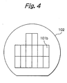
- An embodiment of the ink jet head according to the present invention is formed by a plurality of units 101b, for example, two units 101b as illustrated in Fig. 4 including a monocrystalline silicon substrate. For example, if each unit 101b has a size of about 27mm x 13mm, fourteen units 101b are cut by a dicing blade from an about 10-cm diameter monocrystalline silicon wafer 102.
- nozzle columns 11 and 12 where nozzles 1 are closely arranged in a matrix are provided.
- the nozzle columns 11 and 12 are used for ejecting black ink (or cyan ink) and yellow ink (or magenta ink), respectively.
- the nozzle columns 11 and 12 are connected to ink supply holes 21 and 22, respectively.
- a protruded abutting portion 51 As illustrated in Fig. 5, in each of the units 102b, a protruded abutting portion 51, a recessed abutting portion 52, a protruded abutting portion 53 and a protruded abutting portion 54 are formed. As a result, a relief (recess) 55 is formed between the protruded abutting portions 51 and 53, and a relief (recess) 56 is formed between the abutting portions 52 and 54. Note that the protruded abutting portion 51 has the same shape as the recessed abutting portion 52.
- the average number of defective nozzles 1 is also expected to be 4 among one monocrystalline silicon wafer 102.
- the manufacturing yield can be remarkably increased as compared with the prior art units 101a.
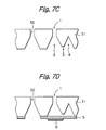
- FIG. 6 is a partially-enlarged view of the unit 101b of Fig. 5, and Figs. 7A, 7B, 7C and 7D are cross-sectional views taken along the line VII-VII of Fig. 6.
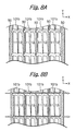
- Figs. 8A and 8B are plan views of the semiconductor wafer of Fig. 4 before and after the separation of units respectively.
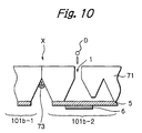
- Fig. 9 is a plan view for explaining the combination of two non-defective units of Figs. 8A and 8B, and Fig. 10 is a cross-sectional view of the abutting portion of the non-defective units of Fig. 9.
- a photoresist pattern 72 is formed by a photolithography process on a front surface of a monocrystalline silicon substrate 71.
- the monocrystalline silicon substrate 71 is etched by a reactive ion etching (RIE) dry process using the photoresist pattern 72 as a mask.
- RIE reactive ion etching
- a photoresist pattern layer (not shown) is formed by a photolithography process on a back surface of the monocrystalline silicon substrate 71. Then, the monocrystalline silicon substrate 71 is etched by an anisotropy wet etching process using the photoresist pattern layer as a mask. As a result, a pressure chamber 2, an ink passage 3 and an ink pool (reservoir) 4 are perforated in the monocrystalline silicon substrate 71, and simultaneously, the edge 50 for the abutting portions 51, 52, 53 and 54 and the reliefs 55 and 56 is completely perforated through the monocrystalline silicon substrate 71. Then, the photoresist pattern layer is removed.
- Fig. 7D note that it is possible to adhere actuators 6 to a wafer-type thin vibration plate 5 before the wafer-type thin vibration plate 5 is adhered to the back surface of the monocrystalline silicon substrate 71.
- the monocrystalline silicon substrate 71 is divided by the edge 50 along the Y-direction into columns of the units 101b, as illustrated in Fig. 8A.
- the monocrystalline silicon substrate 71 is cut by a dicing blade (not shown) along the X-direction. As a result, each of the units 101b is completely separated from each other.
- an ink jet head is constructed by combining two non-defective units 101b-1 and 101b-2. That is, the recessed abutting portion 52 of the non-defective unit 101b-1 abuts against the protruded abutting portion 51 of the non-defective unit 101b-2, while the protruded abutting portion 54 of the non-defective unit 101b-1 abuts against the protruded abutting portion 53 of the non-defective unit 101b-2. In this case, the contact characteristics between the non-defective units 101b-1 and 101b-2 can be improved due to the presence of the reliefs 55 and 56 thereof. Then, the abutting portions of the non-defective units 101b-1 and 101b-2 indicated by arrows X in Fig. 9 are filled with adhesives 73, as illustrated in Fig. 10.
- the combination of the units 101b-1 and 101b-2 can be carried out without an expensive alignment apparatus, which would decrease the manufacturing cost.
- the abutting portions 51, 52, 53 and 54 are formed by a photolithography and etching process, not a dicing blade, the accuracy of the distance between the edge 50 of the abutting portions 51, 52, 53 and 54 and the nozzles 1 of each of the combined units 101b-1 and 101b-2 can be high, i.e., about ⁇ 1 ⁇ m. As a result, the accuracy of the alignment of the nozzles 1 between the combined units 101b-1 and 101b-2 can be high, i.e., about ⁇ 5 ⁇ m.
- the above-mentioned distance accuracy may be ⁇ 6 ⁇ m
- the above-mentioned alignment accuracy may be ⁇ 10 ⁇ m.
- the deviation of droplets among black ink, yellow ink, cyan ink and magenta ink can be decrease, which could not degrade the printing quality.
- one ink jet head is constructed by two combined units 101b-1 and 101b-2; however, one ink jet head can be constructed by three or more combined units. For example, if one unit is formed for one nozzle column, one ink jet head can be constructed by four combined units.
- the substrate 71 is made of monocrystalline silicon; however, the substrate 71 can be made of other crystal or metal. If the substrate 71 is made of metal, a mechanical pressing process or an electroforming process can be performed thereon, so that the nozzles 1 and the like can be formed.
- the nozzles 1 are arranged in a matrix in each of the nozzle columns 11 and 12; however, the arrangement of the nozzles 1 can be staggered in each of the nozzle columns 11 and 12.
- the manufacturing yield of each unit is increased, so that the manufacturing yield of the ink jet head can be increased, which would decrease the manufacturing cost.
Landscapes
- Engineering & Computer Science (AREA)
- Manufacturing & Machinery (AREA)
- Particle Formation And Scattering Control In Inkjet Printers (AREA)
Abstract
Description
Claims (15)
- An ink jet head comprising a plurality of combined units (101b-1, lOlb-2).
- The ink jet head as set forth in claim 1, wherein each of said units comprises:a first protruded abutting portion (51);a recessed abutting portion (52) positioned at an opposite side of said first protruded abutting portion and adapted to said first protruded abutting portion;a second protruded abutting portion (53) on the same side of said first protruded abutting portion; anda third protruded abutting portion (54) positioned on an opposite side of said second protruded abutting portion and adapted to said second protruded abutting portion.
- The ink jet head as set forth in claim 2, wherein the recessed abutting portion and the third protruded abutting portion of one of said units abuts against the first and second protruded abutting portions, respectively, of another of said units.
- The ink jet head as set forth in claim 1,2 or 3, wherein said units carprises:a silicon substrate (71) where nozzles (1), pressure chambers (2), ink passage (3) and ink pools (4) are formed;a vibration plate (5) fixed to said silicon substrate to partition said pressure chambers and said ink passages and said ink pools; andactuators (6), fixed to said vibration plate, each for vibrating a portion of said vibration plate corresponding to one of said nozzles.
- A method for manufacturing an ink jet head, comprising the steps of:forming a plurality of units (101b) in a substrate (102);separating said units from each other; andforming one ink jet head by combining at least two of said units.
- The method as set forth in claim 5, wherein said unit forming step comprises the steps of:forming edge portions (50) along a first direction and nozzles (1) in said substrate (71), said edges dividing said units;forming pressure chambers (2), ink passages (3) and ink pools (4) in said substrate;adhering a vibration plate (5) to said substrate to partition said pressure chambers, said ink passages and said ink pools; andadhering actuators (6) to said vibration plate.
- The method as set forth in claim 6, wherein said edge and nozzle forming step uses a photolithography and dry etching process.
- The method as set forth in claim 6 or 7, wherein said pressure chamber, ink passage and ink pool forming step uses a photolithography and anisotropic etching process.
- The method as set forth in claim 6,7 or 8, wherein said separating step comprises a step of cutting said substrate by a dicing blade along a second direction perpendicular to said first direction.
- The method as set forth in claim 5,6,7,8 or 9, wherein said unit forming step comprises the steps of:forming edge portions (50) along a first direction and nozzles (1) in said substrate (71), said edges dividing said units;forming pressure chambers (2), ink passages (3) and ink pools (4) in said substrate;preparing a vibration plate (5) to which actuators (6) are adhered in advance; andadhering said vibration plate to said substrate to partition said pressure chambers, said ink passages and said ink pools.
- The method as set forth in claim 10, wherein said edge and nozzle forming step uses a photolithography and dry etching process.
- The method as set forth in claim 10 or 11, wherein said pressure chamber, ink passage and ink pool forming step uses a photolithography and anisotropic etching process.
- The method as set forth in claim 10,11 or 12, wherein said separating step comprises a step of cutting said substrate by a dicing blade along a second direction perpendicular to said first direction.
- The method as set forth in any one of claims 5 to 13, wherein each of said units comprises:a first protruded abutting portion (51);a recessed abutting portion (52) positioned at an opposite side of said first protruded abutting portion and adapted to said first protruded abutting portion;a second protruded abutting portion (53) on the same side of said first protruded abutting portion; anda third protruded abutting portion (54) positioned on an opposite side of said second protruded abutting portion and adapted to said second protruded abutting portion.
- The method as set forth in claim 14, wherein said ink jet head forming step abuts the recessed abutting portion and the third protruded abutting portion of one of said units against the first and second protruded abutting portions, respectively, of another of said units.
Applications Claiming Priority (2)
| Application Number | Priority Date | Filing Date | Title |
|---|---|---|---|
| JP2000078898 | 2000-03-21 | ||
| JP2000078898A JP2001260366A (en) | 2000-03-21 | 2000-03-21 | Ink jet recording head and its manufacturing method |
Publications (2)
| Publication Number | Publication Date |
|---|---|
| EP1136269A2 true EP1136269A2 (en) | 2001-09-26 |
| EP1136269A3 EP1136269A3 (en) | 2001-10-04 |
Family
ID=18596240
Family Applications (1)
| Application Number | Title | Priority Date | Filing Date |
|---|---|---|---|
| EP01104029A Withdrawn EP1136269A3 (en) | 2000-03-21 | 2001-02-20 | Ink jet head having a plurality of units and its manufacturing method |
Country Status (4)
| Country | Link |
|---|---|
| US (1) | US6502921B2 (en) |
| EP (1) | EP1136269A3 (en) |
| JP (1) | JP2001260366A (en) |
| CN (1) | CN1224512C (en) |
Cited By (9)
| Publication number | Priority date | Publication date | Assignee | Title |
|---|---|---|---|---|
| WO2003022584A1 (en) | 2001-09-06 | 2003-03-20 | Ricoh Company, Ltd. | Liquid drop discharge head and manufacture method thereof, micro device, ink-jet head, ink cartridge, and ink-jet printing device |
| EP1356939A3 (en) * | 2002-04-25 | 2004-04-28 | Brother Kogyo Kabushiki Kaisha | Ink-jet head and ink-jet printer |
| EP1364790A3 (en) * | 2002-05-21 | 2004-05-12 | Brother Kogyo Kabushiki Kaisha | Ink-jet printing head having a plurality of actuator units and/or a plurality of manifold chambers |
| EP1552932A3 (en) * | 2004-01-10 | 2006-06-07 | Xerox Corporation | Drop emitting device |
| EP1552933A3 (en) * | 2004-01-10 | 2006-06-07 | Xerox Corporation | Drop emitting device |
| EP1552934A3 (en) * | 2004-01-10 | 2006-06-21 | Xerox Corporation | Drop emitting device |
| EP1552930A3 (en) * | 2004-01-10 | 2006-11-29 | Xerox Corporation | Drop emitting device |
| WO2007124768A1 (en) * | 2006-04-28 | 2007-11-08 | Telecom Italia S.P.A. | Ink-jet printhead and manufacturing method thereof |
| CN1636724B (en) * | 2004-01-10 | 2010-11-17 | 施乐公司 | droplet generation device |
Families Citing this family (17)
| Publication number | Priority date | Publication date | Assignee | Title |
|---|---|---|---|---|
| AUPQ455999A0 (en) * | 1999-12-09 | 2000-01-06 | Silverbrook Research Pty Ltd | Memjet four color modular print head packaging |
| US7152945B2 (en) * | 2000-12-07 | 2006-12-26 | Silverbrook Research Pty Ltd | Printhead system having closely arranged printhead modules |
| AUPR224300A0 (en) * | 2000-12-21 | 2001-01-25 | Silverbrook Research Pty. Ltd. | An apparatus (mj72) |
| US6824083B2 (en) * | 2001-06-12 | 2004-11-30 | Fuji Xerox Co., Ltd. | Fluid jetting device, fluid jetting head, and fluid jetting apparatus |
| US6953241B2 (en) | 2001-11-30 | 2005-10-11 | Brother Kogyo Kabushiki Kaisha | Ink-jet head having passage unit and actuator units attached to the passage unit, and ink-jet printer having the ink-jet head |
| KR100428793B1 (en) * | 2002-06-26 | 2004-04-28 | 삼성전자주식회사 | Ink Jet Printer Head And Method Of Fabricating The Same |
| US6880926B2 (en) * | 2002-10-31 | 2005-04-19 | Hewlett-Packard Development Company, L.P. | Circulation through compound slots |
| JP2004337734A (en) * | 2003-05-15 | 2004-12-02 | Seiko Epson Corp | Liquid ejection head and method of manufacturing the same |
| CN1984780B (en) | 2004-04-30 | 2010-09-22 | 富士胶片戴麦提克斯公司 | Droplet Ejector Alignment |
| US7585423B2 (en) * | 2005-05-23 | 2009-09-08 | Canon Kabushiki Kaisha | Liquid discharge head and producing method therefor |
| USD608824S1 (en) * | 2008-01-09 | 2010-01-26 | Panasonic Corporation | Print head for an ink jet printer |
| US8118405B2 (en) * | 2008-12-18 | 2012-02-21 | Eastman Kodak Company | Buttable printhead module and pagewide printhead |
| US8517508B2 (en) | 2009-07-02 | 2013-08-27 | Fujifilm Dimatix, Inc. | Positioning jetting assemblies |
| USD653284S1 (en) | 2009-07-02 | 2012-01-31 | Fujifilm Dimatix, Inc. | Printhead frame |
| USD652446S1 (en) | 2009-07-02 | 2012-01-17 | Fujifilm Dimatix, Inc. | Printhead assembly |
| JP2013193265A (en) | 2012-03-16 | 2013-09-30 | Fuji Xerox Co Ltd | Droplet ejection head and method for manufacturing the same |
| US10336074B1 (en) | 2018-01-18 | 2019-07-02 | Rf Printing Technologies | Inkjet printhead with hierarchically aligned printhead units |
Family Cites Families (14)
| Publication number | Priority date | Publication date | Assignee | Title |
|---|---|---|---|---|
| US4822755A (en) | 1988-04-25 | 1989-04-18 | Xerox Corporation | Method of fabricating large area semiconductor arrays |
| US4878992A (en) | 1988-11-25 | 1989-11-07 | Xerox Corporation | Method of fabricating thermal ink jet printheads |
| US5469199A (en) | 1990-08-16 | 1995-11-21 | Hewlett-Packard Company | Wide inkjet printhead |
| JPH04251750A (en) | 1991-01-28 | 1992-09-08 | Fuji Electric Co Ltd | Ink-jet recording head |
| US5160403A (en) | 1991-08-09 | 1992-11-03 | Xerox Corporation | Precision diced aligning surfaces for devices such as ink jet printheads |
| JP3316597B2 (en) | 1993-01-22 | 2002-08-19 | 富士通株式会社 | Method of manufacturing inkjet head |
| US5956058A (en) | 1993-11-05 | 1999-09-21 | Seiko Epson Corporation | Ink jet print head with improved spacer made from silicon single-crystal substrate |
| US5565900A (en) | 1994-02-04 | 1996-10-15 | Hewlett-Packard Company | Unit print head assembly for ink-jet printing |
| US5572244A (en) | 1994-07-27 | 1996-11-05 | Xerox Corporation | Adhesive-free edge butting for printhead elements |
| US5521125A (en) | 1994-10-28 | 1996-05-28 | Xerox Corporation | Precision dicing of silicon chips from a wafer |
| DE4443254C1 (en) | 1994-11-25 | 1995-12-21 | Francotyp Postalia Gmbh | Ink print head assembly using edge-shooter principle for small high speed computer printer |
| AUPN623795A0 (en) | 1995-10-30 | 1995-11-23 | Eastman Kodak Company | A modular lift print head |
| US5719605A (en) | 1996-11-20 | 1998-02-17 | Lexmark International, Inc. | Large array heater chips for thermal ink jet printheads |
| DE19743804A1 (en) | 1997-10-02 | 1999-04-08 | Politrust Ag | Large format printing using ink-jet printer |
-
2000
- 2000-03-21 JP JP2000078898A patent/JP2001260366A/en active Pending
-
2001
- 2001-02-07 US US09/778,443 patent/US6502921B2/en not_active Expired - Lifetime
- 2001-02-09 CN CNB011036869A patent/CN1224512C/en not_active Expired - Fee Related
- 2001-02-20 EP EP01104029A patent/EP1136269A3/en not_active Withdrawn
Cited By (18)
| Publication number | Priority date | Publication date | Assignee | Title |
|---|---|---|---|---|
| US7090325B2 (en) | 2001-09-06 | 2006-08-15 | Ricoh Company, Ltd. | Liquid drop discharge head and manufacture method thereof, micro device ink-jet head ink cartridge and ink-jet printing device |
| US7731861B2 (en) | 2001-09-06 | 2010-06-08 | Ricoh Company, Ltd. | Liquid drop discharge head and manufacture method thereof, micro device, ink-jet head, ink cartridge, and ink-jet printing device |
| EP1423282A4 (en) * | 2001-09-06 | 2006-06-14 | Ricoh Kk | Liquid drop discharge head and manufacture method thereof, micro device, ink-jet head, ink cartridge, and ink-jet printing device |
| WO2003022584A1 (en) | 2001-09-06 | 2003-03-20 | Ricoh Company, Ltd. | Liquid drop discharge head and manufacture method thereof, micro device, ink-jet head, ink cartridge, and ink-jet printing device |
| EP1356939A3 (en) * | 2002-04-25 | 2004-04-28 | Brother Kogyo Kabushiki Kaisha | Ink-jet head and ink-jet printer |
| US6926382B2 (en) | 2002-04-25 | 2005-08-09 | Brother Kogyo Kabushiki Kaisha | Ink-jet head and ink-jet printer |
| EP1364790A3 (en) * | 2002-05-21 | 2004-05-12 | Brother Kogyo Kabushiki Kaisha | Ink-jet printing head having a plurality of actuator units and/or a plurality of manifold chambers |
| US6994428B2 (en) | 2002-05-21 | 2006-02-07 | Brother Kogyo Kabushiki Kaisha | Ink-jet printing head having a plurality of actuator units and/or a plurality of manifold chambers |
| US7607760B2 (en) | 2002-05-21 | 2009-10-27 | Brother Kogyo Kabushiki Kaisha | Ink-jet printing head having a plurality of actuator units and/or a plurality of manifold chambers |
| EP1552934A3 (en) * | 2004-01-10 | 2006-06-21 | Xerox Corporation | Drop emitting device |
| EP1552930A3 (en) * | 2004-01-10 | 2006-11-29 | Xerox Corporation | Drop emitting device |
| US7222937B2 (en) | 2004-01-10 | 2007-05-29 | Xerox Corporation | Drop generating apparatus |
| EP1552933A3 (en) * | 2004-01-10 | 2006-06-07 | Xerox Corporation | Drop emitting device |
| EP1552932A3 (en) * | 2004-01-10 | 2006-06-07 | Xerox Corporation | Drop emitting device |
| CN1636725B (en) * | 2004-01-10 | 2010-11-17 | 施乐公司 | Drop emitting device |
| CN1636724B (en) * | 2004-01-10 | 2010-11-17 | 施乐公司 | droplet generation device |
| WO2007124768A1 (en) * | 2006-04-28 | 2007-11-08 | Telecom Italia S.P.A. | Ink-jet printhead and manufacturing method thereof |
| US8128203B2 (en) | 2006-04-28 | 2012-03-06 | Telecom Italia S.P.A. | Ink-jet printhead and manufacturing method thereof |
Also Published As
| Publication number | Publication date |
|---|---|
| US20010024217A1 (en) | 2001-09-27 |
| CN1314252A (en) | 2001-09-26 |
| CN1224512C (en) | 2005-10-26 |
| US6502921B2 (en) | 2003-01-07 |
| EP1136269A3 (en) | 2001-10-04 |
| JP2001260366A (en) | 2001-09-25 |
Similar Documents
| Publication | Publication Date | Title |
|---|---|---|
| US6502921B2 (en) | Ink jet head having a plurality of units and its manufacturing method | |
| CN101121319B (en) | Printhead | |
| EP1321294B1 (en) | Piezoelectric ink-jet printhead and method for manufacturing the same | |
| EP0376514B1 (en) | Method of fabricating large array semiconductor devices | |
| US6931702B2 (en) | Inkjet recording head and method for manufacturing the same | |
| EP1693206B1 (en) | Piezoelectric inkjet printhead and method of manufacturing the same | |
| JPH02229050A (en) | Method for manufacturing ink-jet print head | |
| JPH01166965A (en) | Manufacture of ink-jet printing head | |
| US10029466B2 (en) | Ink-jet recording head, recording element substrate, method for manufacturing ink-jet recording head, and method for manufacturing recording element substrate | |
| JPH1058685A (en) | Ink jet print head having channels arranged on surface in silicon | |
| US10081187B2 (en) | Method of manufacturing an ink-jet printhead having frusto-pyramidal shaped nozzles | |
| EP1681169B1 (en) | Piezoelectric inkjet printhead and method of manufacturing the same | |
| CN100478178C (en) | Liquid drop discharge head and manufacture method thereof, micro device, ink-jet head, ink cartridge, and ink-jet printing device | |
| JP2010240825A (en) | MEMS device having uniform film and manufacturing method thereof | |
| JP3985329B2 (en) | Inkjet head manufacturing method | |
| US8152280B2 (en) | Method of making an inkjet printhead | |
| KR100528349B1 (en) | Piezo-electric type inkjet printhead and manufacturing method threrof | |
| WO1998047712A1 (en) | Nozzle plate for an ink jet print head | |
| KR20050084752A (en) | Fabrication method for inkjet head and inkjet recording apparatus | |
| US8714707B2 (en) | Method of making hole in substrate, substrate, nozzle plate and ink jet head | |
| KR100561865B1 (en) | Piezoelectric inkjet printheads and manufacturing method thereof | |
| JP2021059054A (en) | Substrate manufacturing method and element substrate manufacturing method | |
| JP2006130850A (en) | Ink jet head and method of manufacturing ink jet head | |
| HK1113113B (en) | Printhead | |
| HK1078832B (en) | Printhead |
Legal Events
| Date | Code | Title | Description |
|---|---|---|---|
| PUAI | Public reference made under article 153(3) epc to a published international application that has entered the european phase |
Free format text: ORIGINAL CODE: 0009012 |
|
| PUAL | Search report despatched |
Free format text: ORIGINAL CODE: 0009013 |
|
| AK | Designated contracting states |
Kind code of ref document: A2 Designated state(s): DE GB Kind code of ref document: A2 Designated state(s): AT BE CH CY DE DK ES FI FR GB GR IE IT LI LU MC NL PT SE TR |
|
| AX | Request for extension of the european patent |
Free format text: AL;LT;LV;MK;RO;SI |
|
| AK | Designated contracting states |
Kind code of ref document: A3 Designated state(s): AT BE CH CY DE DK ES FI FR GB GR IE IT LI LU MC NL PT SE TR |
|
| AX | Request for extension of the european patent |
Free format text: AL;LT;LV;MK;RO;SI |
|
| RIC1 | Information provided on ipc code assigned before grant |
Free format text: 7B 41J 2/14 A, 7B 41J 2/16 B, 7H 01L 21/78 B |
|
| 17P | Request for examination filed |
Effective date: 20010829 |
|
| 17Q | First examination report despatched |
Effective date: 20020115 |
|
| AKX | Designation fees paid |
Free format text: DE GB |
|
| RAP1 | Party data changed (applicant data changed or rights of an application transferred) |
Owner name: FUJI XEROX CO., LTD. |
|
| STAA | Information on the status of an ep patent application or granted ep patent |
Free format text: STATUS: THE APPLICATION IS DEEMED TO BE WITHDRAWN |
|
| 18D | Application deemed to be withdrawn |
Effective date: 20030417 |