EP1134833A2 - Method for adjusting frequency of attenuation pole of dual-mode band pass filter - Google Patents
Method for adjusting frequency of attenuation pole of dual-mode band pass filter Download PDFInfo
- Publication number
- EP1134833A2 EP1134833A2 EP01105147A EP01105147A EP1134833A2 EP 1134833 A2 EP1134833 A2 EP 1134833A2 EP 01105147 A EP01105147 A EP 01105147A EP 01105147 A EP01105147 A EP 01105147A EP 1134833 A2 EP1134833 A2 EP 1134833A2
- Authority
- EP
- European Patent Office
- Prior art keywords
- metal film
- input
- dielectric substrate
- band pass
- dual
- Prior art date
- Legal status (The legal status is an assumption and is not a legal conclusion. Google has not performed a legal analysis and makes no representation as to the accuracy of the status listed.)
- Granted
Links
- 238000000034 method Methods 0.000 title claims abstract description 36
- 230000008878 coupling Effects 0.000 claims abstract description 152
- 238000010168 coupling process Methods 0.000 claims abstract description 152
- 238000005859 coupling reaction Methods 0.000 claims abstract description 152
- 239000002184 metal Substances 0.000 claims abstract description 126
- 239000000758 substrate Substances 0.000 claims abstract description 65
- QNRATNLHPGXHMA-XZHTYLCXSA-N (r)-(6-ethoxyquinolin-4-yl)-[(2s,4s,5r)-5-ethyl-1-azabicyclo[2.2.2]octan-2-yl]methanol;hydrochloride Chemical compound Cl.C([C@H]([C@H](C1)CC)C2)CN1[C@@H]2[C@H](O)C1=CC=NC2=CC=C(OCC)C=C21 QNRATNLHPGXHMA-XZHTYLCXSA-N 0.000 description 6
- 239000000463 material Substances 0.000 description 4
- 230000005540 biological transmission Effects 0.000 description 2
- 239000003989 dielectric material Substances 0.000 description 2
- 125000001153 fluoro group Chemical group F* 0.000 description 2
- 239000011347 resin Substances 0.000 description 2
- 229920005989 resin Polymers 0.000 description 2
- 239000000919 ceramic Substances 0.000 description 1
- 229910052681 coesite Inorganic materials 0.000 description 1
- 238000004891 communication Methods 0.000 description 1
- 229910052906 cristobalite Inorganic materials 0.000 description 1
- 230000009977 dual effect Effects 0.000 description 1
- 230000000694 effects Effects 0.000 description 1
- 238000012986 modification Methods 0.000 description 1
- 230000004048 modification Effects 0.000 description 1
- 230000035699 permeability Effects 0.000 description 1
- 239000000377 silicon dioxide Substances 0.000 description 1
- VYPSYNLAJGMNEJ-UHFFFAOYSA-N silicon dioxide Inorganic materials O=[Si]=O VYPSYNLAJGMNEJ-UHFFFAOYSA-N 0.000 description 1
- 229910052682 stishovite Inorganic materials 0.000 description 1
- 229910052905 tridymite Inorganic materials 0.000 description 1
Images





Classifications
-
- H—ELECTRICITY
- H01—ELECTRIC ELEMENTS
- H01P—WAVEGUIDES; RESONATORS, LINES, OR OTHER DEVICES OF THE WAVEGUIDE TYPE
- H01P7/00—Resonators of the waveguide type
- H01P7/08—Strip line resonators
-
- H—ELECTRICITY
- H01—ELECTRIC ELEMENTS
- H01P—WAVEGUIDES; RESONATORS, LINES, OR OTHER DEVICES OF THE WAVEGUIDE TYPE
- H01P1/00—Auxiliary devices
- H01P1/20—Frequency-selective devices, e.g. filters
- H01P1/201—Filters for transverse electromagnetic waves
- H01P1/203—Strip line filters
- H01P1/20327—Electromagnetic interstage coupling
- H01P1/20354—Non-comb or non-interdigital filters
- H01P1/20381—Special shape resonators
Definitions
- the present invention relates to a dual-mode band pass filter incorporated as a band filter, for example, in a communication apparatus used in a range of a microwave band to a millimeter-wave band.
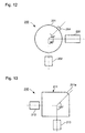
- FIG. 12 and 13 shows a schematic plan view for illustrating a conventional dual-mode band pass filter.
- a circular-shaped conductive film 201 is formed on a dielectric substrate (not shown).
- the conductive film 201 is coupled to input/output coupling circuits 202 and 203 disposed at an angle of 90 degrees.
- a top-end open stub 204 is formed in a position making an angle of 45 degrees with respect to the part where the input/output coupling circuit 203 is arranged.
- a substantially square conductive film 211 is formed on a dielectric substrate.
- the conductive film 211 is coupled to input/output coupling circuits 212 and 213 disposed at an angle of 90 degree.
- a corner positioned at an angle of 135 degrees with respect to the input/output coupling circuit 213 is cut away to form a cut-away part 211a.
- a dual-mode filter using a loop-shaped conductive film there is provided a dual-mode filter using a loop-shaped conductive film. That is, in each of Japanese Unexamined Patent Application Publication No. 9-139612 and Japanese Unexamined Patent Application Publication No. 9-162610, there is a dual-mode filter.
- This dual-mode filter incorporates a loop-shaped ring transmission line.
- input/output coupling circuits are arranged at a central angle of 90 degrees therebetween, and a top-end open stub is disposed at a part of the ring transmission line.
- the circular or square conductive film pattern has a structure coupling the input/output coupling circuits at each of the above specified angles, the coupling strength between the two resonance modes cannot be increased.
- the pass band for the filter cannot be broadened.
- the conductive film 201 is circular.
- the conductive film 211 is substantially square. That is, both conductive films 201 and 211 have limited configurations.
- the frequency band is determined by the dimensions of the circular or square conductive film, particularly, the position of an attenuation pole (the frequency) cannot be easily adjusted.
- this band pass filter With this band pass filter, the above-described problems of the conventional art can be solved, and the size of the filter can be reduced. In addition, the coupling strength between two resonance modes can be increased. Furthermore, the dual-mode band pass filter of the invention can have a great deal of the freedom of design.
- a method for adjusting the frequency of an attenuation pole of a dual-mode band pass filter includes a step of forming a metal film on a surface of a dielectric substrate or in the dielectric substrate, a step of arranging a ground electrode in a such a manner that the ground electrode overlaps with the metal film via at least a part of the dielectric substrate in a thickness direction of the dielectric substrate, a step of forming at least one opening in the metal film to couple two resonance modes, a step of coupling an input/output coupling circuit to the metal film, a step of forming a coupling portion capacitively coupled to a perimeter of the metal film via a gap, and a step of forming an input/output portion coupled to the coupling portion, and the input/output coupling circuit includes the coupling portion and the input/output portion.
- at least one of the coupling portion and the input/output portion is moved in a direction along the perimeter
- a method for adjusting the frequency of an attenuation pole of a dual-mode band pass filter includes a step of forming a metal film on a surface of a dielectric substrate or in the dielectric substrate, a step of arranging a ground electrode in a such a manner that the ground electrode overlaps with the metal film via at least a part of the dielectric substrate in a thickness direction of the dielectric substrate, a step of forming at least one opening in the metal film to couple two resonance modes, and a step of forming an input/output coupling circuit coupled to the metal film.
- the input/output coupling circuit is formed by one of a strip line and a microstrip line. One end of the strip line or the microstrip line is directly and electrically connected to the metal film. A point for coupling the strip line or the microstrip line to the metal film is moved on the perimeter of the metal film.
- a method for adjusting the frequency of an attenuation pole of a dual-mode band pass filter includes a step of forming a metal film on a surface of a dielectric substrate or in the dielectric substrate, a step of arranging a ground electrode in a such a manner that the ground electrode overlaps with the metal film via at least a part of the dielectric substrate in a thickness direction of the dielectric substrate, a step of forming at least one opening in the metal film to couple two resonance modes, and a step of forming an input/output coupling circuit coupled to the metal film.
- the metal film and the input/output coupling circuit are formed on different layers of the dielectric substrate.
- the input/output coupling circuit overlaps with the metal film via the dielectric layer so that the input/output coupling circuit is capacitively coupled to the metal film.
- a point for coupling the input/output coupling circuit to the metal film is moved along the perimeter of the metal film on the dielectric layer.
- a method for adjusting the frequency of an attenuation pole of a dual-mode band pass filter includes a step of forming a metal film on a surface of a dielectric substrate or in the dielectric substrate, a step of arranging a ground electrode in a such a manner that the ground electrode overlaps with the metal film via at least a part of the dielectric substrate in a thickness direction of the dielectric substrate, a step of forming at least one opening in the metal film to couple two resonance modes, a step of forming an input/output coupling circuit coupled to the metal film, and a step of forming an insulating layer having a via-hole electrode between the input/output coupling circuit and the metal film.
- one end of the via-hole electrode is electrically connected to the input/output coupling circuit and the other end thereof is electrically connected to the metal film.
- Positions for connecting the via-hole electrode to the input/output coupling circuit and the metal film are moved along the perimeter of the metal film.
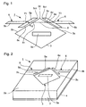
- Fig. 1 is a schematic plan view for illustrating a method for adjusting the frequency of an attenuation pole of a dual-mode band pass filter according to a first embodiment of the invention.
- Fig. 2 is a perspective view thereof.
- a dual-mode band pass filter 1 has a dielectric substrate 2 having a configuration of a rectangular plate.
- the dielectric substrate 2 is made of a fluoro resin having a permeability er of 2.58.
- a dielectric material forming a dielectric substrate is not limited to the fluoro resin.
- a dielectric material such as Ba0-Al 2 O 3 -SiO 2 ceramic can be used as an appropriate material.
- the thickness of the dielectric substrate 2 is not specifically determined. In this embodiment, the thickness thereof is set to be 350 ⁇ m.
- a metal film 3 for forming a resonator is disposed on an upper surface 2a of the dielectric substrate 2.
- the metal film 3 is partially disposed on the dielectric substrate 2.
- the metal film 3 has a rhombic shape.
- an opening 3a is formed in the metal film 3.
- the opening 3a has a rectangular-planar shape, whose lengthwise direction is parallel to the direction of a longer diagonal line of the metal film 3.
- each sideline of the rhombic shape of the metal film 3 is 15 mm in length, the longer diagonal line thereof is 24 mm in length, and the shorter diagonal line thereof is 18 mm in length.
- the longer sideline of the opening 3a is 9 mm in length and the shorter sideline thereof is 0.2 mm in length.
- the opening 3a is formed in such a manner that the center of the opening 3a coincides with the center of the metal film 3.
- the dimensions of the metal film 3 and opening 3a, and the position of the opening 3a are not restricted to those shown in the above case, and can be appropriately changed according to a desirable central frequency and a desirable bandwidth when necessary.
- a ground electrode 4 is disposed on the entire lower surface of the dielectric substrate 2.
- each of input/output coupling circuits 5 and 6 is separated by a predetermined gap from each of a pair of sidelines 3b and 3c having a large interior angle therebetween.
- the input/output coupling circuits 5 and 6 are arranged by disposing metal films made of the same material as that of the metal film 3 on the dielectric substrate 2.
- the input/output coupling circuit 5 has a coupling portion 5a and an input/output portion 5b
- the input/output coupling circuit 6 has a coupling portion 6a and an input/output portion 6b.
- the coupling portions 5a and 6a have parallelogrammic shapes in Fig. 1.
- the coupling portion 5a has an edge 5c parallel to the sideline 3b of the metal film 3 and the coupling portion 6a has an edge 6c parallel to the sideline 3c thereof.
- the sideline 5c of the coupling portion 5a faces the sideline 3b of the metal film 3 and the sideline 6c of the coupling portion 6a faces the sideline 3c thereof via predetermined gaps g, respectively. With this arrangement, the coupling portions 5a and 6a are capacitively coupled to the metal film 3.
- the input/output portion 5b is coupled to the coupling portion 5a and the input/output portion 6b is coupled to the coupling portion 6a, and the input/output portions 5b and 6b are electrically connected to external circuits.
- an input voltage is applied between the input/output coupling circuit 5 and the ground electrode 4, with the result that an output voltage is extracted between the input/output coupling circuit 6 and the ground electrode 4.
- the metal film 3 is rhombic and the opening 3a is formed therein, two occurring resonance modes are coupled with each other so that the filter of the first embodiment can act as a dual-mode band pass filter.
- the dual-mode band pass filter 1 there are obtained the resonance mode occurring in the direction of a virtual straight line connecting the center of the coupling portion 5a of the input/output coupling circuit 5 and the center of the coupling portion 6a of the input/output coupling circuit 6 and the resonance mode occurring in a direction orthogonal to the virtual straight line.
- the resonance current in the direction orthogonal to the virtual straight line is stopped by the opening 3a.
- the resonant frequency in the direction orthogonal to the virtual straight line moves to the low-frequency side.
- the size of the opening 3a is adjusted so that the amount of a movement to the low-frequency side is controlled. As a result, the two resonance modes can be coupled with each other.
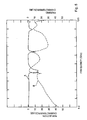
- Fig. 3 shows an example of the frequency characteristics of the band pass filter according to the embodiment.
- a solid line A indicates reflection characteristics
- a broken line B indicates passing characteristics.
- the reflection characteristics are indicated by solid lines A and the passing characteristics are indicated by broken lines B.
- a band pass filter in which a band indicated by an arrow C is the pass band. That is, in the dual-mode band pass filter 1 of the embodiment, by forming the opening 3a in the metal film 3, the two resonance modes are coupled with each other so that the frequency characteristics for serving as the dual-mode band pass filter can be obtained.
- the attenuation-pole frequency is adjusted by moving the positions where the input/output portion 5b is coupled to the coupling portion 5a and the input/output portion 6b is coupled to the coupling portion 6a, along the sidelines 3b and 3c of the metal film 3, respectively. This will be illustrated with reference to Figs. 4 and 5.
- the coupling portions 5a and 6a are formed in the same manner. Specifically, the coupling portion 5a has the edge 5c and the coupling portion 6a has the edge 6c, and each of the edges 5c and 6c is separated from each of the sidelines 3b and 3c by a gap g of 0.1 mm in length. Each of the edges 5c and 6c is 13 mm in length in parallel to each of the sidelines 3b and 3c from each of ends 5c 1 and 6c 1 separated by the gap g from a top 3d.
- a coupling point Y 1 of the input/output portion 5b and the coupling portion 5a and a coupling point Y 2 of the input/output portion 6b and the coupling portion 6a are determined in such a manner that each of positions X 1 and X 2 where the virtual straight line X connecting the input/output portions 5b and 6b crosses the sidelines 3b and 3c is set to be at a distance of 5 mm from the top 3d.
- the coupling point of the input/output portion 5b and the coupling portion 5a and the coupling point of the input/output portion 6b and the coupling portion 6a are determined in such a manner that the virtual line are set to be in positions at distances of 7 mm and 9 mm from the top 3d along the sidelines 3b and 3c.
- the filter 1 can act as a dual-mode band pass filter. Additionally, it is found that the attenuation-pole frequency can be changed by moving the positions of the coupling points.
- the adjustment of the attenuation-pole frequency of the dual-mode band pass filter 1 can be performed by changing the positions of the coupling point of the input/output portion 5b and the coupling portion 5a and the coupling point of the input/output portion 6b and the coupling portion 6a.
- the rhombic metal film 3 having the same size is formed on the dielectric substrate and the opening 3a is formed in the dielectric substrate.
- the coupling portions 5a and 6a and the input/output portions 5b and 6b are arranged in such a manner that the position of the coupling point Y 1 of the coupling portion 5a and the input/output portion 5b and the position of the coupling point Y 2 of the coupling portion 6a and the input/output portion 6b are deviated from the previous positions.
- the dual-mode band pass filter 1 can have a desirable attenuation-pole frequency.
- this embodiment can facilitate the adjustment of the attenuation-pole frequency of the dual-mode band pass filter.
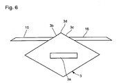
- Fig. 6 is a schematic plan view for illustrating a method for adjusting the frequency of an attenuation pole of a dual-mode band pass filter according to a second embodiment of the present invention.
- Fig. 6 shows only a metal film and input/output coupling circuits disposed on a dielectric substrate (not shown), in the dual-mode band pass filter. This is equivalent to Fig. 1 shown in the first embodiment.
- the dielectric substrate and a ground electrode formed on a lower surface of the dielectric substrate are formed in the same manner as those of the dual-mode band pass filter 1 according to the first embodiment. Thus, the explanation thereof in the first embodiment is also applied to the second embodiment.
- the metal film 3 and the opening 3a are arranged in the same manner as those used in the first embodiment.
- the input/output coupling circuits of the second embodiment are formed by strip lines 15 and 16 directly and electrically connected to the sidelines 3b and 3c of the metal film 3.
- the dielectric substrate, the metal film 3, and the opening 3a are formed of the same material in the same dimensions as the material and dimensions used in the first embodiment.
- points connecting the strip lines 15 and 16 to the sidelines 3b and 3c of the metal film 3, that is, coupling points are set at positions of 5 mm, 7 mm, and 9 mm from the top 3d to constitute three kinds of dual-mode band pass filters 1.
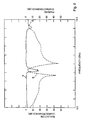
- Figs. 7 to 9 show the frequency characteristics of these dual-mode band pass filters.
- each filter can also act as a dual-mode band pass filter.
- the attenuation-pole frequency can be changed, thereby facilitating the adjustment of the attenuation-pole frequency.
- the embodiment can also be applied to a microstrip line structure.
- the positions of the coupling portions 5a and 6a are fixed and the positions of the input/output portions 5b and 6b are changed.
- the input/output coupling circuits 15 and 16 formed by inductance coils are directly coupled to the sidelines 3b and 3c of the metal film 3, and the positions of the coupling points are changed to adjust the attenuation-pole frequency.
- the present invention is not restricted to the first and second embodiments and can variously be modified according to the structure and coupling manner of the input/output coupling circuits.
- Figs. 10A and 10B are a schematic plan view and a partially cut-away front sectional view for illustrating a method for adjusting the frequency of an attenuation pole of a dual-mode band pass filter according to a third embodiment of the present invention.
- a metal film 3 is embedded in a dielectric substrate 22.
- input/output coupling circuits 25 and 26 are formed on an upper surface 22a of the dielectric substrate 22.
- Coupling portions 25a and 26a of the input/output coupling circuits 25 and 26 are arranged in such a manner that the portions 25a and 26a overlap with the metal film 3 via a dielectric substrate layer.
- the input/output coupling circuits are flush with the metal film 3 and the coupling portions 5a and 6a are capacitively coupled to the metal film 3.
- the input/output coupling circuits 25 and 26 may be formed in positions different from that of the metal film 3.
- the dielectric substrate 22 has a multilayer structure formed by stacking a plurality of dielectric layers, and the coupling portions 25a and 26a are capacitively coupled to the metal film 3 via the dielectric-substrate layer.
- the attenuation-pole frequency can be changed.
- the coupling portions 5a and 6a are fixed and the positions of the input/output portions 5b and 6b are deviated.
- the frequency of the attenuation pole can be adjusted.
- both of the above two ways may be used together.
- the frequency of the attenuation pole can be adjusted by changing the positions of the coupling portions 25a and 26a of the input/output coupling circuits 25 and 26 and/or by deviating positions at which the input/output portions 25b and 26b are coupled to the coupling portions 25a and 26a.
- the metal film may be embedded in the dielectric substrate.
- the input/output coupling circuits it is not necessary to form the circuits on the upper surface of the dielectric substrate.
- the input/output coupling circuits may be formed in the dielectric substrate.
- the ground electrode 4 it is not necessary to form the ground electrode 4, as shown in the first embodiment, on the lower surface of the dielectric substrate.
- the ground electrode 4 may be formed in the dielectric substrate.
- Figs. 11A and 11B are a schematic plan view and a partially cut-away front sectional view for illustrating a method for adjusting the frequency of an attenuation pole according to a fourth embodiment of the present invention.
- a metal film 3 is embedded in a dielectric substrate 2, and input/output coupling circuits 35 and 36 formed by inductance coils are disposed on the dielectric substrate 2.
- the input/output coupling circuits 35 and 36 are directly and electrically connected to the metal film 3 via the via-hole electrodes 35a and 36a.
- the strip lines 15 and 16 as the input/output coupling circuits are connected to the metal film 3 in such a manner that the strip lines 15 and 16 are flush with the metal film 3.
- the input/output coupling circuits 35 and 36 may be positioned at a height different from the height at which the metal film 3 is positioned.
- the frequency of the attenuation pole can be changed by changing the positions of the via-hole electrodes 35a and 36a, that is, by changing the positions of points at which the input/output coupling circuits 35 and 36 are coupled to the metal film 3.
- the input/output coupling circuits may be embedded in the substrate.
- the metal film 3 has a rhombic shape.
- the planar shape of the metal film 3 used in the present invention is not restricted to a rhombus, and any of other polygons such as a square, a rectangular, and a triangle, or any shape having a random perimeter may be arbitrarily used.
- the metal film for forming a resonator is disposed on the dielectric substrate, and at least one opening is formed in the metal film to couple two resonance modes.
- the positions of the points at which the input/output coupling circuits are coupled to the metal film are not specifically restricted.
- band characteristics required as a dual-mode band pass filter can be obtained.
- the input/output coupling circuits have the coupling portions, which are capacitively coupled to the metal film, and the input/output portions. Since at least either the coupling portions or the input/output portions are moved in a direction along the perimeter of the metal film facing via the gap, the frequency of the attenuation pole can be easily adjusted.
- the input/output coupling circuits are formed by inductors.
- One end of each of the input/output coupling circuits is directly and electrically connected to the metal film, and the points at which the input/output coupling circuits are coupled to the metal film are moved along the perimeter of the metal film.
- a dielectric multilayer structure between the metal film and the input/output coupling circuits.
- the input/output coupling circuits overlap with the metal film via the dielectric multilayer structure to be capacitively coupled to the metal film.
- the frequency of an attenuation pole of the dual-mode band pass filter can easily be adjusted by moving the positions of the input/output coupling circuits along the perimeter of the metal film on the dielectric multilayer structure.
- the insulating layer having via-hole electrodes is disposed between the input/output coupling circuits and the metal film.
- One-side ends of the via-hole electrodes are electrically connected to the input/output coupling circuits, and the other ends thereof are electrically connected to the metal film.
- the conventional dual-mode band pass filter there are limitations to the shape of the metal film forming a resonator and the positions of the points at which the input/output coupling circuits are coupled to the metal film.
- the dual-mode band pass filter according to each of the first to fourth aspects of the invention there are no such limitations to the dual-mode band pass filter according to each of the first to fourth aspects of the invention.
- the freedom of designing the dual-mode band pass filter can be greatly increased.
- the frequency of the attenuation pole can be easily adjusted not only by changing the dimensions of the metal film and the opening but also by changing the positions of the points coupling the input/output coupling circuits to the metal film, as shown in the present invention.
Landscapes
- Physics & Mathematics (AREA)
- Electromagnetism (AREA)
- Control Of Motors That Do Not Use Commutators (AREA)
Abstract
Description
Claims (4)
- A method for adjusting the frequency of an attenuation pole of a dual-mode band pass filter (1), the method comprising the steps of:forming a metal film (3) on a surface of a dielectric substrate (2) or in the dielectric substrate (2);arranging a ground electrode (4) in a such a manner that the ground electrode (4) overlaps with the metal film (3) via at least a part of the dielectric substrate (2) in a thickness direction of the dielectric substrate (2);forming at least one opening (3a) in the metal film (3) to couple two resonance modes;forming an input/output coupling circuit (5, 6) coupled to the metal film (3);forming a coupling portion (5a, 6a) capacitively coupled to a perimeter of the metal film (3) via a gap (g); andforming an input/output portion (5b, 6b) coupled to the coupling portion (5a, 6a), the input/output coupling circuit (5, 6) comprising the coupling portion (5a, 6a) and the input/output portion (5b, 6b);wherein at least one of the coupling portion (5a, 6a) and the input/output portion (5b, 6b) is moved in a direction along the perimeter of the metal film (3) for adjusting the frequency of the attenuation pole.
- A method for adjusting the frequency of an attenuation pole of a dual-mode band pass filter, the method comprising the steps of:forming a metal film (3) on a surface of a dielectric substrate (2) or in the dielectric substrate (2);arranging a ground electrode (4) in a such a manner that the ground electrode (4) overlaps with the metal film (3) via at least a part of the dielectric substrate (2) in a thickness direction of the dielectric substrate (2);forming at least one opening (3a) in the metal film (3) to couple two resonance modes; andforming an input/output coupling circuit (5, 6) coupled to the metal film (3);wherein the input/output coupling circuit is formed by one of a strip line (15, 16) and a microstrip line, one end of the strip line (15, 16) or the microstrip line being directly and electrically connected to the metal film (3), and a coupling point at which the strip line (15, 16) or the microstrip line is connected to the metal film (3) is moved on the perimeter of the metal film (3) for adjusting the frequency of the attenuation pole.
- A method for adjusting the frequency of an attenuation pole of a dual-mode band pass filter (21), the method comprising the steps of:forming a metal film (3) on a surface of a dielectric substrate (22) having a multilayer structure or in the dielectric substrate (22);arranging a ground electrode (4) in a such a manner that the ground electrode (4) overlaps with the metal film (3) via at least a part of the dielectric substrate (22) in a thickness direction of the dielectric substrate (22);forming at least one opening (3a) in the metal film (3) to couple two resonance modes; andforming an input/output coupling circuit (25, 26) coupled to the metal film (3);wherein the metal film (3) and the input/output coupling circuit (25, 26) are formed on different layers of the dielectric substrate (22), the input/output coupling circuit (25, 26) overlapping with the metal film (3) via the dielectric layer so that the input/output coupling circuit (25, 26) is capacitively coupled to the metal film (3), and a point for coupling the input/output coupling circuit (25, 26) to the metal film (3) is moved along the perimeter of the metal film (3) on the dielectric layer for adjusting the frequency of the attenuation pole.
- A method for adjusting the frequency of an attenuation pole of a dual-mode band pass filter, the method comprising the steps of:forming a metal film (3) on a surface of a dielectric substrate (2) or in the dielectric substrate (2);arranging a ground electrode (4) in a such a manner that the ground electrode (4) overlaps with the metal film (3) via at least a part of the dielectric substrate (2) in a thickness direction of the dielectric substrate (2);forming at least one opening (3a) in the metal film (3) to couple two resonance modes;forming an input/output coupling circuit (35, 36) coupled to the metal film (3) ; andforming an insulating layer having a via-hole electrode (35a, 36a) between the input/output coupling circuit (35, 36) and the metal film (3);wherein one end of the via-hole electrode (35a, 36a) is electrically connected to the input/output coupling circuit (35, 36) and the other end thereof is electrically connected to the metal film (3), positions for connecting the via-hole electrode (35a, 36a) to the input/output coupling circuit (35, 36) and the metal film (3) being moved along the perimeter of the metal film (3) for adjusting the frequency of the attenuation pole.
Applications Claiming Priority (2)
| Application Number | Priority Date | Filing Date | Title |
|---|---|---|---|
| JP2000068795A JP3575378B2 (en) | 2000-03-13 | 2000-03-13 | Frequency adjustment method of attenuation pole of dual mode bandpass filter |
| JP2000068795 | 2000-03-13 |
Publications (3)
| Publication Number | Publication Date |
|---|---|
| EP1134833A2 true EP1134833A2 (en) | 2001-09-19 |
| EP1134833A3 EP1134833A3 (en) | 2003-02-26 |
| EP1134833B1 EP1134833B1 (en) | 2007-11-07 |
Family
ID=18587798
Family Applications (1)
| Application Number | Title | Priority Date | Filing Date |
|---|---|---|---|
| EP01105147A Expired - Lifetime EP1134833B1 (en) | 2000-03-13 | 2001-03-02 | Method for adjusting frequency of attenuation pole of dual-mode band pass filter |
Country Status (5)
| Country | Link |
|---|---|
| US (1) | US6812813B2 (en) |
| EP (1) | EP1134833B1 (en) |
| JP (1) | JP3575378B2 (en) |
| KR (1) | KR100394802B1 (en) |
| DE (1) | DE60131212T2 (en) |
Cited By (2)
| Publication number | Priority date | Publication date | Assignee | Title |
|---|---|---|---|---|
| CN110034360A (en) * | 2019-03-26 | 2019-07-19 | 西安理工大学 | Open the three frequency filter of minor matters straight-flanked ring of short-circuit Stepped Impedance line load |
| CN111613857A (en) * | 2020-05-25 | 2020-09-01 | 南京师范大学 | A Novel Dual-pass Band Filter Coupler Using Double-layer Slotted Circular Patches |
Families Citing this family (11)
| Publication number | Priority date | Publication date | Assignee | Title |
|---|---|---|---|---|
| JP3395754B2 (en) * | 2000-02-24 | 2003-04-14 | 株式会社村田製作所 | Dual-mode bandpass filter |
| JP5171819B2 (en) * | 2007-06-14 | 2013-03-27 | 京セラ株式会社 | DC blocking circuit, hybrid circuit device, transmitter, receiver, transceiver, and radar device |
| TWI381574B (en) * | 2008-09-24 | 2013-01-01 | Univ Nat Changhua Education | Dual band bandpass filter |
| US8884722B2 (en) * | 2009-01-29 | 2014-11-11 | Baharak Mohajer-Iravani | Inductive coupling in transverse electromagnetic mode |
| US8081050B2 (en) * | 2009-02-25 | 2011-12-20 | Alcatel Lucent | Multilayer planar tunable filter |
| KR101138479B1 (en) * | 2010-10-14 | 2012-04-25 | 삼성전기주식회사 | Coupling structure for multi-layered chip filter, and multi-layered chip filter with the structure |
| KR101364770B1 (en) | 2012-10-23 | 2014-02-17 | 주식회사 선단테크 | Dual-mode microstrip band pass filter with dual feed |
| CN104022318B (en) * | 2014-05-16 | 2017-03-01 | 南通大学 | Bandwidth and the individually controllable multilamellar Dual-mode two-way band balun wave filter of operating frequency |
| TWI573314B (en) * | 2015-05-27 | 2017-03-01 | 鴻海精密工業股份有限公司 | Band-pass filter |
| CA3106112A1 (en) | 2018-07-11 | 2020-01-16 | Cld Western Property Holdings Ltd. | Frequency-selective planar radio filter |
| CN112445075B (en) * | 2019-08-30 | 2023-12-29 | 上海微电子装备(集团)股份有限公司 | Flat reed, micro-motion device and photoetching machine |
Family Cites Families (12)
| Publication number | Priority date | Publication date | Assignee | Title |
|---|---|---|---|---|
| JPS4939542B1 (en) * | 1969-08-01 | 1974-10-26 | ||
| JPS5641001B1 (en) * | 1971-04-30 | 1981-09-25 | ||
| JPS5118454A (en) | 1975-06-24 | 1976-02-14 | Tokyo Shibaura Electric Co | MAIKUROHADENJIKYO SHINKI |
| JPH039502A (en) | 1989-06-07 | 1991-01-17 | Murata Mfg Co Ltd | Manufacture of organic positive characteristics thermistor |
| JP3009502B2 (en) | 1991-06-11 | 2000-02-14 | マツダ株式会社 | Vehicle power transmission |
| US5136268A (en) * | 1991-04-19 | 1992-08-04 | Space Systems/Loral, Inc. | Miniature dual mode planar filters |
| EP0571777B1 (en) * | 1992-04-30 | 1998-07-01 | Matsushita Electric Industrial Co., Ltd. | Stripline dual mode ring resonator and band-pass filter composed thereof. |
| JP3048509B2 (en) | 1993-12-27 | 2000-06-05 | 松下電器産業株式会社 | High frequency circuit element |
| US6239674B1 (en) * | 1993-12-27 | 2001-05-29 | Matsushita Electric Industrial Co., Ltd | Elliptical resonator with an input/output capacitive gap |
| JP3304724B2 (en) | 1995-11-16 | 2002-07-22 | 松下電器産業株式会社 | Dual mode filter |
| JPH09162610A (en) | 1995-12-14 | 1997-06-20 | Matsushita Electric Ind Co Ltd | Dual mode resonator |
| JP3277834B2 (en) * | 1996-12-11 | 2002-04-22 | 松下電器産業株式会社 | Planar bandpass filter |
-
2000
- 2000-03-13 JP JP2000068795A patent/JP3575378B2/en not_active Expired - Fee Related
-
2001
- 2001-03-02 EP EP01105147A patent/EP1134833B1/en not_active Expired - Lifetime
- 2001-03-02 DE DE60131212T patent/DE60131212T2/en not_active Expired - Lifetime
- 2001-03-12 KR KR10-2001-0012621A patent/KR100394802B1/en not_active Expired - Fee Related
- 2001-03-14 US US09/805,648 patent/US6812813B2/en not_active Expired - Fee Related
Cited By (2)
| Publication number | Priority date | Publication date | Assignee | Title |
|---|---|---|---|---|
| CN110034360A (en) * | 2019-03-26 | 2019-07-19 | 西安理工大学 | Open the three frequency filter of minor matters straight-flanked ring of short-circuit Stepped Impedance line load |
| CN111613857A (en) * | 2020-05-25 | 2020-09-01 | 南京师范大学 | A Novel Dual-pass Band Filter Coupler Using Double-layer Slotted Circular Patches |
Also Published As
| Publication number | Publication date |
|---|---|
| KR100394802B1 (en) | 2003-08-14 |
| JP2001257506A (en) | 2001-09-21 |
| US6812813B2 (en) | 2004-11-02 |
| JP3575378B2 (en) | 2004-10-13 |
| KR20010091980A (en) | 2001-10-23 |
| EP1134833A3 (en) | 2003-02-26 |
| EP1134833B1 (en) | 2007-11-07 |
| DE60131212T2 (en) | 2008-08-28 |
| DE60131212D1 (en) | 2007-12-20 |
| US20010024151A1 (en) | 2001-09-27 |
Similar Documents
| Publication | Publication Date | Title |
|---|---|---|
| EP1134833B1 (en) | Method for adjusting frequency of attenuation pole of dual-mode band pass filter | |
| US6630875B2 (en) | Dual-mode band-pass filter | |
| EP1942549B1 (en) | Dual-mode bandpass filter | |
| EP1170819B1 (en) | Dual mode band pass filter | |
| JPH0856107A (en) | Dual mode resonator | |
| JP4242738B2 (en) | Multilayer bandpass filter | |
| JP3395753B2 (en) | Method of manufacturing bandpass filter and bandpass filter | |
| JP4442066B2 (en) | Dual-mode bandpass filter, characteristic adjustment method for dual-mode bandpass filter, duplexer, and wireless communication apparatus | |
| US6608537B2 (en) | Band-pass filter | |
| JP2001203513A (en) | High frequency dielectric resonator | |
| JPH08181506A (en) | Dielectric filter | |
| JP2002368503A (en) | Method for adjusting characteristic for band-pass filter | |
| JP3469339B2 (en) | High frequency filter | |
| JPH11136001A (en) | Stacked stripline filter with improved frequency characteristics | |
| JP2002232205A (en) | Multilayer dielectric filter | |
| JP2002261506A (en) | Laminated dielectric filter and frequency adjustment method thereof | |
| JP2001284920A (en) | Dual mode band-pass filter and frequency control method for attenuation electrode therefor |
Legal Events
| Date | Code | Title | Description |
|---|---|---|---|
| PUAI | Public reference made under article 153(3) epc to a published international application that has entered the european phase |
Free format text: ORIGINAL CODE: 0009012 |
|
| 17P | Request for examination filed |
Effective date: 20010302 |
|
| AK | Designated contracting states |
Kind code of ref document: A2 Designated state(s): AT BE CH CY DE DK ES FI FR GB GR IE IT LI LU MC NL PT SE TR |
|
| AX | Request for extension of the european patent |
Free format text: AL;LT;LV;MK;RO;SI |
|
| PUAL | Search report despatched |
Free format text: ORIGINAL CODE: 0009013 |
|
| AK | Designated contracting states |
Kind code of ref document: A3 Designated state(s): AT BE CH CY DE DK ES FI FR GB GR IE IT LI LU MC NL PT SE TR |
|
| AX | Request for extension of the european patent |
Extension state: AL LT LV MK RO SI |
|
| AKX | Designation fees paid |
Designated state(s): DE FR GB |
|
| GRAP | Despatch of communication of intention to grant a patent |
Free format text: ORIGINAL CODE: EPIDOSNIGR1 |
|
| RAP1 | Party data changed (applicant data changed or rights of an application transferred) |
Owner name: MURATA MANUFACTURING CO., LTD. |
|
| GRAS | Grant fee paid |
Free format text: ORIGINAL CODE: EPIDOSNIGR3 |
|
| GRAA | (expected) grant |
Free format text: ORIGINAL CODE: 0009210 |
|
| AK | Designated contracting states |
Kind code of ref document: B1 Designated state(s): DE FR GB |
|
| REG | Reference to a national code |
Ref country code: GB Ref legal event code: FG4D |
|
| REF | Corresponds to: |
Ref document number: 60131212 Country of ref document: DE Date of ref document: 20071220 Kind code of ref document: P |
|
| ET | Fr: translation filed | ||
| PLBE | No opposition filed within time limit |
Free format text: ORIGINAL CODE: 0009261 |
|
| STAA | Information on the status of an ep patent application or granted ep patent |
Free format text: STATUS: NO OPPOSITION FILED WITHIN TIME LIMIT |
|
| 26N | No opposition filed |
Effective date: 20080808 |
|
| PGFP | Annual fee paid to national office [announced via postgrant information from national office to epo] |
Ref country code: FR Payment date: 20120319 Year of fee payment: 12 |
|
| PGFP | Annual fee paid to national office [announced via postgrant information from national office to epo] |
Ref country code: GB Payment date: 20120301 Year of fee payment: 12 |
|
| PGFP | Annual fee paid to national office [announced via postgrant information from national office to epo] |
Ref country code: DE Payment date: 20120404 Year of fee payment: 12 |
|
| GBPC | Gb: european patent ceased through non-payment of renewal fee |
Effective date: 20130302 |
|
| REG | Reference to a national code |
Ref country code: FR Ref legal event code: ST Effective date: 20131129 |
|
| REG | Reference to a national code |
Ref country code: DE Ref legal event code: R119 Ref document number: 60131212 Country of ref document: DE Effective date: 20131001 |
|
| PG25 | Lapsed in a contracting state [announced via postgrant information from national office to epo] |
Ref country code: FR Free format text: LAPSE BECAUSE OF NON-PAYMENT OF DUE FEES Effective date: 20130402 Ref country code: GB Free format text: LAPSE BECAUSE OF NON-PAYMENT OF DUE FEES Effective date: 20130302 Ref country code: DE Free format text: LAPSE BECAUSE OF NON-PAYMENT OF DUE FEES Effective date: 20131001 |