EP1134823A1 - A method for forming a thin film - Google Patents
A method for forming a thin film Download PDFInfo
- Publication number
- EP1134823A1 EP1134823A1 EP01106733A EP01106733A EP1134823A1 EP 1134823 A1 EP1134823 A1 EP 1134823A1 EP 01106733 A EP01106733 A EP 01106733A EP 01106733 A EP01106733 A EP 01106733A EP 1134823 A1 EP1134823 A1 EP 1134823A1
- Authority
- EP
- European Patent Office
- Prior art keywords
- thin film
- solution
- anode electrode
- powders
- metallic
- Prior art date
- Legal status (The legal status is an assumption and is not a legal conclusion. Google has not performed a legal analysis and makes no representation as to the accuracy of the status listed.)
- Withdrawn
Links
- 239000010409 thin film Substances 0.000 title claims abstract description 51
- 238000000034 method Methods 0.000 title claims description 37
- 239000000843 powder Substances 0.000 claims abstract description 38
- 150000001875 compounds Chemical class 0.000 claims abstract description 30
- XLYOFNOQVPJJNP-UHFFFAOYSA-N water Chemical compound O XLYOFNOQVPJJNP-UHFFFAOYSA-N 0.000 claims abstract description 8
- 239000012153 distilled water Substances 0.000 claims abstract description 4
- 238000002844 melting Methods 0.000 claims abstract description 4
- 230000008018 melting Effects 0.000 claims abstract description 4
- 229910000765 intermetallic Inorganic materials 0.000 claims description 16
- 239000000758 substrate Substances 0.000 claims description 13
- 239000011148 porous material Substances 0.000 claims description 2
- GLXDVVHUTZTUQK-UHFFFAOYSA-M lithium;hydroxide;hydrate Chemical compound [Li+].O.[OH-] GLXDVVHUTZTUQK-UHFFFAOYSA-M 0.000 claims 1
- BASFCYQUMIYNBI-UHFFFAOYSA-N platinum Chemical compound [Pt] BASFCYQUMIYNBI-UHFFFAOYSA-N 0.000 abstract description 26
- 229910052697 platinum Inorganic materials 0.000 abstract description 13
- WMFOQBRAJBCJND-UHFFFAOYSA-M Lithium hydroxide Chemical compound [Li+].[OH-] WMFOQBRAJBCJND-UHFFFAOYSA-M 0.000 abstract description 10
- 229910032387 LiCoO2 Inorganic materials 0.000 abstract description 7
- 239000013078 crystal Substances 0.000 abstract description 3
- 238000010438 heat treatment Methods 0.000 description 5
- 239000000463 material Substances 0.000 description 5
- 238000002441 X-ray diffraction Methods 0.000 description 4
- 238000005229 chemical vapour deposition Methods 0.000 description 4
- 239000002245 particle Substances 0.000 description 3
- 238000003980 solgel method Methods 0.000 description 3
- 239000007772 electrode material Substances 0.000 description 2
- 238000010304 firing Methods 0.000 description 2
- 238000001228 spectrum Methods 0.000 description 2
- 239000000126 substance Substances 0.000 description 2
- HBBGRARXTFLTSG-UHFFFAOYSA-N Lithium ion Chemical compound [Li+] HBBGRARXTFLTSG-UHFFFAOYSA-N 0.000 description 1
- 239000004809 Teflon Substances 0.000 description 1
- 229920006362 Teflon® Polymers 0.000 description 1
- 239000003575 carbonaceous material Substances 0.000 description 1
- 239000010941 cobalt Substances 0.000 description 1
- 229910017052 cobalt Inorganic materials 0.000 description 1
- GUTLYIVDDKVIGB-UHFFFAOYSA-N cobalt atom Chemical compound [Co] GUTLYIVDDKVIGB-UHFFFAOYSA-N 0.000 description 1
- 230000007613 environmental effect Effects 0.000 description 1
- 239000004744 fabric Substances 0.000 description 1
- 229910001416 lithium ion Inorganic materials 0.000 description 1
- 238000004020 luminiscence type Methods 0.000 description 1
- 239000013528 metallic particle Substances 0.000 description 1
- 239000000203 mixture Substances 0.000 description 1
- 230000004048 modification Effects 0.000 description 1
- 238000012986 modification Methods 0.000 description 1
- 239000007800 oxidant agent Substances 0.000 description 1
- 239000000123 paper Substances 0.000 description 1
- AKHNMLFCWUSKQB-UHFFFAOYSA-L sodium thiosulfate Chemical compound [Na+].[Na+].[O-]S([O-])(=O)=S AKHNMLFCWUSKQB-UHFFFAOYSA-L 0.000 description 1
Images

Classifications
-
- H—ELECTRICITY
- H01—ELECTRIC ELEMENTS
- H01M—PROCESSES OR MEANS, e.g. BATTERIES, FOR THE DIRECT CONVERSION OF CHEMICAL ENERGY INTO ELECTRICAL ENERGY
- H01M4/00—Electrodes
- H01M4/02—Electrodes composed of, or comprising, active material
- H01M4/04—Processes of manufacture in general
- H01M4/0402—Methods of deposition of the material
- H01M4/0421—Methods of deposition of the material involving vapour deposition
- H01M4/0423—Physical vapour deposition
-
- C—CHEMISTRY; METALLURGY
- C25—ELECTROLYTIC OR ELECTROPHORETIC PROCESSES; APPARATUS THEREFOR
- C25D—PROCESSES FOR THE ELECTROLYTIC OR ELECTROPHORETIC PRODUCTION OF COATINGS; ELECTROFORMING; APPARATUS THEREFOR
- C25D9/00—Electrolytic coating other than with metals
- C25D9/04—Electrolytic coating other than with metals with inorganic materials
- C25D9/06—Electrolytic coating other than with metals with inorganic materials by anodic processes
-
- H—ELECTRICITY
- H01—ELECTRIC ELEMENTS
- H01M—PROCESSES OR MEANS, e.g. BATTERIES, FOR THE DIRECT CONVERSION OF CHEMICAL ENERGY INTO ELECTRICAL ENERGY
- H01M4/00—Electrodes
- H01M4/02—Electrodes composed of, or comprising, active material
- H01M4/04—Processes of manufacture in general
-
- H—ELECTRICITY
- H01—ELECTRIC ELEMENTS
- H01M—PROCESSES OR MEANS, e.g. BATTERIES, FOR THE DIRECT CONVERSION OF CHEMICAL ENERGY INTO ELECTRICAL ENERGY
- H01M4/00—Electrodes
- H01M4/02—Electrodes composed of, or comprising, active material
- H01M4/04—Processes of manufacture in general
- H01M4/0402—Methods of deposition of the material
- H01M4/0404—Methods of deposition of the material by coating on electrode collectors
-
- H—ELECTRICITY
- H01—ELECTRIC ELEMENTS
- H01M—PROCESSES OR MEANS, e.g. BATTERIES, FOR THE DIRECT CONVERSION OF CHEMICAL ENERGY INTO ELECTRICAL ENERGY
- H01M4/00—Electrodes
- H01M4/02—Electrodes composed of, or comprising, active material
- H01M4/04—Processes of manufacture in general
- H01M4/0402—Methods of deposition of the material
- H01M4/0421—Methods of deposition of the material involving vapour deposition
- H01M4/0428—Chemical vapour deposition
-
- H—ELECTRICITY
- H01—ELECTRIC ELEMENTS
- H01M—PROCESSES OR MEANS, e.g. BATTERIES, FOR THE DIRECT CONVERSION OF CHEMICAL ENERGY INTO ELECTRICAL ENERGY
- H01M4/00—Electrodes
- H01M4/02—Electrodes composed of, or comprising, active material
- H01M4/04—Processes of manufacture in general
- H01M4/0438—Processes of manufacture in general by electrochemical processing
- H01M4/045—Electrochemical coating; Electrochemical impregnation
- H01M4/0452—Electrochemical coating; Electrochemical impregnation from solutions
-
- H—ELECTRICITY
- H01—ELECTRIC ELEMENTS
- H01M—PROCESSES OR MEANS, e.g. BATTERIES, FOR THE DIRECT CONVERSION OF CHEMICAL ENERGY INTO ELECTRICAL ENERGY
- H01M4/00—Electrodes
- H01M4/02—Electrodes composed of, or comprising, active material
- H01M4/04—Processes of manufacture in general
- H01M4/0483—Processes of manufacture in general by methods including the handling of a melt
-
- Y—GENERAL TAGGING OF NEW TECHNOLOGICAL DEVELOPMENTS; GENERAL TAGGING OF CROSS-SECTIONAL TECHNOLOGIES SPANNING OVER SEVERAL SECTIONS OF THE IPC; TECHNICAL SUBJECTS COVERED BY FORMER USPC CROSS-REFERENCE ART COLLECTIONS [XRACs] AND DIGESTS
- Y02—TECHNOLOGIES OR APPLICATIONS FOR MITIGATION OR ADAPTATION AGAINST CLIMATE CHANGE
- Y02E—REDUCTION OF GREENHOUSE GAS [GHG] EMISSIONS, RELATED TO ENERGY GENERATION, TRANSMISSION OR DISTRIBUTION
- Y02E60/00—Enabling technologies; Technologies with a potential or indirect contribution to GHG emissions mitigation
- Y02E60/10—Energy storage using batteries
Definitions
- This invention relates to a method for forming a thin film, particularly to a method for forming a thin film suitable for a secondary battery field usable for mobile electronic device and electric automobiles.
- a sol-gel method, a CVD method or a PVD method is employed as a thin film-forming method.
- These methods require a multistage process including a heating process, a high vacuum condition, or a high energy condition accompanied with a substrate-heating process or a plasma-generating process. Therefore, those methods require large scale and complicate apparatus, resulting in large cost and complicate operationality in use.
- This invention relates to a method for forming a thin film comprising the steps of:
- the inventors related to the present invention have been intensely studied for developing a new thin film-forming method not including a high energy process. As a result, they have found out surprisingly that when a reactive solution is made of a blended solution in which a given substance is dissolved and a given metallic powders added into the blended solution, and then, a given voltage is applied between a cathode electrode and an anode electrode provided in the reactive solution, a compound thin film composed of the components of the blended solution and the metallic powders is formed on the anode electrode, which is not pre-treated and heated. Then, since the compound thin film exhibits crystallinity, it is turned out that the components are reacted and synthesized on the anode electrode to form the crystalline compound thin film.
- a substrate made of a porous material is set on a surface of the anode electrode opposite to the cathode electrode.
- the components of the blended solution and the metallic powder or metallic compound powders pass through the substrate freely, and arrive at the surfaces of the substrate. Therefore, the components are directly reacted on the substrate, and thus, the compound thin film is directly synthesized from the above components on the surfaces of the substrate.
- the compound thin film is not formed. Therefore, if the anode electrode is formed in a predetermined patterned shape, the compound thin film can be synthesized in a given pattern corresponding to the patterned anode electrode.
- the crystalline compound thin film can be formed on the anode electrode or the porous substrate without a pre-treating process, etc.
- the compound thin film can be synthesized without a high energy process, but an additional energy process such as a heating process is not always excluded.
- the reactive solution is heated to 60-300°C, particularly 100-200°C.
- the compound thin film can be uniformly synthesized on the anode electrode or the porous substrate provided on the anode electrode and the density of the compound thin film can be enhanced, irrespective of the kind of the reactive solution, that is, the kinds of the blended solution and the metallic powders or metallic compound powders.
- a thin film is formed of a given solution and dried, and then, heated and fired at 500-800°C to synthesize a desired crystalline compound thin film. Therefore, the high temperature firing process is required.
- the additional energy process of the thin film-forming method of the present invention is very small in energy, compared with the above high energy process in the sol-gel method or the CVD method.
- the amplitude of the voltage to be applied between the cathode electrode and the anode electrode is not restricted only if the compound thin film can be uniformly synthesized directly on the anode electrode or the porous substrate provided on the anode electrode.
- the amplitude of the voltage is selected so that a current with a current density of 0.01-10 mA/cm 3 is flown in between the electrodes.
- the reactive solution may be flown at a flow rate of 0.1-100 mL/minute. In both cases, the compound thin film can be synthesized uniformly according to the present invention.
- the kinds of the blended solution and the metallic powders or metallic compound powders are determined on the kind of the compound thin film to be formed. Moreover, the concentration of the blended solution and the amount of the metallic powders or metallic compound powders are determined on the forming rate and the thickness of the compound thin film.
- metal powders or "metallic compound powders” means “metallic particles” or “metallic compound particles” having an average particle diameter of 0.01-100 ⁇ m, respectively.
- the cathode electrode and the anode electrode may be made of a well known electrode material such as carbon material, platinum material or cobalt material.
- the porous base material may be made of Teflon, paper or cloth.
- the compound thin film can be formed in a given patterned shape, corresponding to the patterned thin film.
- the anode electrode may have such a patterned shape as a dot-like shape, a lattice-like shape or a comb-like shape.
- the thin film-forming method can be applied for any compound thin film, but may be preferably for the Co-based oxide thin film such as LiCoO 2 , which is used as an electrode material of a lithium ion secondary battery, a V-based oxide thin film, a Mn-based oxide thin film, a Fe-based oxide thin film, a W-based oxide thin film and a Mo-based oxide thin film, which are employed as a fluorescent material and a luminescence material.
- the Co-based oxide thin film such as LiCoO 2 , which is used as an electrode material of a lithium ion secondary battery
- V-based oxide thin film a Mn-based oxide thin film
- a Fe-based oxide thin film a W-based oxide thin film
- Mo-based oxide thin film which are employed as a fluorescent material and a luminescence material.
- a well known oxidizer such as Na 2 S 2 O 3 or H 2 O 2 can be preferably used.
- the reactive solution was charged into an autoclave, and heated to 200°C.
- diffraction peaks from LiCoO 2 are observed on the surface of the platinum electrode. That is, it is turned out that a compound thin film, made of LiCoO 2 crystal composed of Li element of blended solution and Co element of the metallic powders, is formed on the platinum electrode.
- Example 2 Except that the concentration of LiOH in the blended solution was set to 5 mol/L and the current density between the platinum electrodes was set to 0.05 mA/cm 3 , the same processes as in Example 1 were carried out. Then, the surfaces of the platinum electrode constituting the anode electrode was examined by X-ray diffraction, as in Example 1. The thus obtained result is shown in Fig. 2.
- a compound thin film made of LiCoO 2 crystal composed of Li element of blended solution and Co element of the metallic powders, is formed on the platinum electrode.
- the blended solution is made by melting only one kind of LiOH ⁇ H 2 O into distilled water.
- the blended solution may be made of a water solution in which two or more substances are melted, depending on the composition of the compound thin film.
- two or more kinds of metallic powders or metallic compound powders may be employed.
- a compound thin film can be directly synthesized on an anode electrode or a porous substrate provided on the anode electrode without a high energy condition including a high temperature substrate-heating process and a plasma-generating process in a conventional CVD method or PVD method.
- a new thin film-forming method not including the high energy condition can be provided.
Landscapes
- Chemical & Material Sciences (AREA)
- Engineering & Computer Science (AREA)
- Chemical Kinetics & Catalysis (AREA)
- Electrochemistry (AREA)
- Manufacturing & Machinery (AREA)
- General Chemical & Material Sciences (AREA)
- Inorganic Chemistry (AREA)
- Materials Engineering (AREA)
- Metallurgy (AREA)
- Organic Chemistry (AREA)
- Battery Electrode And Active Subsutance (AREA)
Abstract
Description
- This invention relates to a method for forming a thin film, particularly to a method for forming a thin film suitable for a secondary battery field usable for mobile electronic device and electric automobiles.
- So far, a sol-gel method, a CVD method or a PVD method is employed as a thin film-forming method. These methods require a multistage process including a heating process, a high vacuum condition, or a high energy condition accompanied with a substrate-heating process or a plasma-generating process. Therefore, those methods require large scale and complicate apparatus, resulting in large cost and complicate operationality in use.
- Moreover, the above high energy condition runs counter to global environmental protection, resource saving and energy saving. Therefore, a new thin film-forming method without the above high energy condition has been desired.
- It is an object of the present invention to provide a new thin film-forming method not including a high energy condition due to firing, heating or plasma generation.
- This invention relates to a method for forming a thin film comprising the steps of:
- preparing a reactive solution by adding metallic powders or metallic compound powders into a blended solution,
- setting an anode electrode and a cathode electrode in the reactive solution,
- applying a given voltage between the anode electrode and the cathode electrode, thereby to synthesize a compound thin film including the components of the blended solution and the metallic powders or the metallic compound powders on the anode electrode.
-
- The inventors related to the present invention have been intensely studied for developing a new thin film-forming method not including a high energy process. As a result, they have found out surprisingly that when a reactive solution is made of a blended solution in which a given substance is dissolved and a given metallic powders added into the blended solution, and then, a given voltage is applied between a cathode electrode and an anode electrode provided in the reactive solution, a compound thin film composed of the components of the blended solution and the metallic powders is formed on the anode electrode, which is not pre-treated and heated. Then, since the compound thin film exhibits crystallinity, it is turned out that the components are reacted and synthesized on the anode electrode to form the crystalline compound thin film.
- On the other hand, when only a blended solution incorporating components of a compound thin film to be formed is employed without metallic powders or metallic compound powders, the compound thin film is not formed or is formed very slowly on the anode electrode.
- That is, it is required in this invention to use a reactive solution made of a given blended solution and given metallic powders or metallic compound powders. As a result, a compound thin film is made of the components of the blended solution and the metallic powders or metallic compound powders.
- This invention has been established on the basis of the discovery of the above fact.
- In a preferred embodiment of the thin film-forming method of the present invention, a substrate made of a porous material is set on a surface of the anode electrode opposite to the cathode electrode. In this case, the components of the blended solution and the metallic powder or metallic compound powders pass through the substrate freely, and arrive at the surfaces of the substrate. Therefore, the components are directly reacted on the substrate, and thus, the compound thin film is directly synthesized from the above components on the surfaces of the substrate.
- If the given voltage is not applied to the reactive solution, the compound thin film is not formed. Therefore, if the anode electrode is formed in a predetermined patterned shape, the compound thin film can be synthesized in a given pattern corresponding to the patterned anode electrode.
- According to the thin film-forming method of the present invention, the crystalline compound thin film can be formed on the anode electrode or the porous substrate without a pre-treating process, etc.
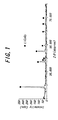
- The invention will be more particularly described with reference to the accompanying drawings:
- Fig. 1 is a graph showing the X-ray diffraction spectrum of a LiCoO2 thin film synthesized by the thin film-forming method of the present invention, and
- Fig. 2 is a graph showing the X-ray diffraction spectrum of another LiCoO2 thin film synthesized by the thin film-forming method of the present invention.
-
- The invention will be described in detail as follows.
- According to the present invention, the compound thin film can be synthesized without a high energy process, but an additional energy process such as a heating process is not always excluded. Preferably, the reactive solution is heated to 60-300°C, particularly 100-200°C. Thereby, the compound thin film can be uniformly synthesized on the anode electrode or the porous substrate provided on the anode electrode and the density of the compound thin film can be enhanced, irrespective of the kind of the reactive solution, that is, the kinds of the blended solution and the metallic powders or metallic compound powders.
- In a conventional wet thin film-forming method such as a sol-gel method, a thin film is formed of a given solution and dried, and then, heated and fired at 500-800°C to synthesize a desired crystalline compound thin film. Therefore, the high temperature firing process is required.
- Moreover, in the CVD method, a substrate is normally heated to 500-800°C. Therefore, the additional energy process of the thin film-forming method of the present invention is very small in energy, compared with the above high energy process in the sol-gel method or the CVD method.
- The amplitude of the voltage to be applied between the cathode electrode and the anode electrode is not restricted only if the compound thin film can be uniformly synthesized directly on the anode electrode or the porous substrate provided on the anode electrode. Preferably, the amplitude of the voltage is selected so that a current with a current density of 0.01-10 mA/cm3 is flown in between the electrodes. Thereby, the components of the blended solution and the metallic powders or the metallic compound powders are dissociated in their respective enough amounts to synthesize the compound thin film uniformly, irrespective of the kinds of the blended solution and the metallic powders or metallic compound powders.
- In the thin film-forming method of the present invention, it is not always required to stand still the reactive solution. The reactive solution may be flown at a flow rate of 0.1-100 mL/minute. In both cases, the compound thin film can be synthesized uniformly according to the present invention.
- The kinds of the blended solution and the metallic powders or metallic compound powders are determined on the kind of the compound thin film to be formed. Moreover, the concentration of the blended solution and the amount of the metallic powders or metallic compound powders are determined on the forming rate and the thickness of the compound thin film.
- In this invention, the wording "metallic powders" or "metallic compound powders" means "metallic particles" or "metallic compound particles" having an average particle diameter of 0.01-100 µm, respectively.
- Moreover, the cathode electrode and the anode electrode may be made of a well known electrode material such as carbon material, platinum material or cobalt material.
- The porous base material may be made of Teflon, paper or cloth.
- In the case of forming a thin film on the porous substrate, if the anode electrode is formed in a predetermined patterned shape as mentioned above, the compound thin film can be formed in a given patterned shape, corresponding to the patterned thin film. The anode electrode may have such a patterned shape as a dot-like shape, a lattice-like shape or a comb-like shape.
- The thin film-forming method can be applied for any compound thin film, but may be preferably for the Co-based oxide thin film such as LiCoO2, which is used as an electrode material of a lithium ion secondary battery, a V-based oxide thin film, a Mn-based oxide thin film, a Fe-based oxide thin film, a W-based oxide thin film and a Mo-based oxide thin film, which are employed as a fluorescent material and a luminescence material.
- In this case, a well known oxidizer such as Na2S2O3 or H2O2 can be preferably used.
- This invention will be concretely described with reference to the following examples.
- First of all, 300 mL of a blended solution with a concentration of 7 mol/L of LiOH was made by melting LiOH·H2O into distilled water. Then, 0.2 g of Co metallic powders with an average particle diameter of 2 µm was added into the blended solution to make a reactive solution.
- Then, the reactive solution was charged into an autoclave, and heated to 200°C. A pair of platinum electrodes, which were opposite each other, were set in the reactive solution as the anode electrode and the cathode electrode. Then, a given voltage was applied between the platinum electrodes to flow a current with a current density of 2.5 mA/cm2 therebetween.
- Two hours later, the platinum electrodes were taken out of the autoclave, and then, the surface of the platinum electrode constituting the anode electrode was examined by X-ray diffraction. The thus obtained result is shown in Fig. 1.
- As is apparent from Fig. 1, diffraction peaks from LiCoO2 are observed on the surface of the platinum electrode. That is, it is turned out that a compound thin film, made of LiCoO2 crystal composed of Li element of blended solution and Co element of the metallic powders, is formed on the platinum electrode.
- Except that the concentration of LiOH in the blended solution was set to 5 mol/L and the current density between the platinum electrodes was set to 0.05 mA/cm3, the same processes as in Example 1 were carried out. Then, the surfaces of the platinum electrode constituting the anode electrode was examined by X-ray diffraction, as in Example 1. The thus obtained result is shown in Fig. 2.
- As is apparent from Fig. 2, it is also turned out that a compound thin film, made of LiCoO2 crystal composed of Li element of blended solution and Co element of the metallic powders, is formed on the platinum electrode.
- Although this invention bas been described in detail with reference to the above examples, this invention is not limited to the above disclosure and every kind of variation and modification may be made without departing from the scope of the present invention.
- For example, in the above examples, the blended solution is made by melting only one kind of LiOH·H2O into distilled water. However, the blended solution may be made of a water solution in which two or more substances are melted, depending on the composition of the compound thin film. Moreover, two or more kinds of metallic powders or metallic compound powders may be employed.
- According to the present invention, a compound thin film can be directly synthesized on an anode electrode or a porous substrate provided on the anode electrode without a high energy condition including a high temperature substrate-heating process and a plasma-generating process in a conventional CVD method or PVD method. As a result, a new thin film-forming method not including the high energy condition can be provided.
Claims (5)
- A method for forming a thin film comprising the steps of:preparing a reactive solution by adding metallic powders or metallic compound powders into a blended solution,setting an anode electrode and a cathode electrode in the reactive solution,applying a given voltage between the anode electrode and the cathode electrode, thereby to synthesize a compound thin film including the components of the blended solution and the metallic powders or the metallic compound powders on the anode electrode.
- A method for forming a thin film as defined in claim 1, wherein the reactive solution is heated and held at 60-300°C.
- A method for forming a thin film as defined in claim 1 or 2, further comprising the step of setting a substrate made of a porous material at least onto a surface of the anode electrode opposite to the cathode electrode, whereby the compound thin film is synthesized on the substrate.
- A method for forming a thin film as defined in any one of claims 1-3, wherein the anode electrode has a predetermined patterned shape, and the compound thin film is formed in a given patterned shape, corresponding to the patterned shape of the anode electrode.
- A method for forming a thin film as defined in any one of claims 1-4, wherein the reactive solution is composed of the blended solution made by melting LiOH H2O into distilled water and Co metallic powders added into the blended solution, and an oxide thin film including Li element and Co element is synthesized.
Applications Claiming Priority (2)
| Application Number | Priority Date | Filing Date | Title |
|---|---|---|---|
| JP2000076578A JP3353066B2 (en) | 2000-03-17 | 2000-03-17 | Thin film formation method |
| JP2000076578 | 2000-03-17 |
Publications (1)
| Publication Number | Publication Date |
|---|---|
| EP1134823A1 true EP1134823A1 (en) | 2001-09-19 |
Family
ID=18594299
Family Applications (1)
| Application Number | Title | Priority Date | Filing Date |
|---|---|---|---|
| EP01106733A Withdrawn EP1134823A1 (en) | 2000-03-17 | 2001-03-16 | A method for forming a thin film |
Country Status (3)
| Country | Link |
|---|---|
| US (1) | US6440292B2 (en) |
| EP (1) | EP1134823A1 (en) |
| JP (1) | JP3353066B2 (en) |
Families Citing this family (4)
| Publication number | Priority date | Publication date | Assignee | Title |
|---|---|---|---|---|
| JP4407211B2 (en) * | 2003-09-02 | 2010-02-03 | 日産自動車株式会社 | Nonaqueous electrolyte secondary battery |
| DK3172169T3 (en) | 2014-07-22 | 2021-10-18 | Xerion Advanced Battery Corp | LITHIERED TRANSITIONAL METAL OXIDES |
| KR101984722B1 (en) | 2016-07-21 | 2019-05-31 | 주식회사 엘지화학 | Lithium Secondary Battery containing Cathod Active Material Synthesizing Lithium Cobalt Oxide, Manufacturing Method Thereof |
| US20190100850A1 (en) | 2017-10-03 | 2019-04-04 | Xerion Advanced Battery Corporation | Electroplating Transitional Metal Oxides |
Citations (3)
| Publication number | Priority date | Publication date | Assignee | Title |
|---|---|---|---|---|
| US3520780A (en) * | 1967-05-11 | 1970-07-14 | Xerox Corp | Magnesium electrodeposition |
| EP0319489A1 (en) * | 1987-11-27 | 1989-06-07 | Permelec Electrode Ltd | Electrode catalyst and method for production thereof |
| US5597661A (en) * | 1992-10-23 | 1997-01-28 | Showa Denko K.K. | Solid polymer electrolyte, battery and solid-state electric double layer capacitor using the same as well as processes for the manufacture thereof |
Family Cites Families (3)
| Publication number | Priority date | Publication date | Assignee | Title |
|---|---|---|---|---|
| JP3387314B2 (en) * | 1996-04-26 | 2003-03-17 | 松下電器産業株式会社 | Manufacturing method of hydrogen storage alloy electrode |
| JPH10326619A (en) * | 1997-03-27 | 1998-12-08 | Japan Storage Battery Co Ltd | Method for producing positive electrode active material for non-aqueous electrolyte battery and battery provided with the positive electrode active material |
| JP3353070B2 (en) | 2000-03-17 | 2002-12-03 | 東京工業大学長 | Thin film formation method |
-
2000
- 2000-03-17 JP JP2000076578A patent/JP3353066B2/en not_active Expired - Lifetime
-
2001
- 2001-03-16 EP EP01106733A patent/EP1134823A1/en not_active Withdrawn
- 2001-03-16 US US09/810,781 patent/US6440292B2/en not_active Expired - Fee Related
Patent Citations (3)
| Publication number | Priority date | Publication date | Assignee | Title |
|---|---|---|---|---|
| US3520780A (en) * | 1967-05-11 | 1970-07-14 | Xerox Corp | Magnesium electrodeposition |
| EP0319489A1 (en) * | 1987-11-27 | 1989-06-07 | Permelec Electrode Ltd | Electrode catalyst and method for production thereof |
| US5597661A (en) * | 1992-10-23 | 1997-01-28 | Showa Denko K.K. | Solid polymer electrolyte, battery and solid-state electric double layer capacitor using the same as well as processes for the manufacture thereof |
Non-Patent Citations (2)
| Title |
|---|
| HAN K -S ET AL: "SIMULTANEOUS AND DIRECT FABRICATION OF LITHIUM COBALT OXIDE FILM AND POWDER USING SOFT SOLUTION PROCESSING AT 100øC", ELECTROCHEMICAL AND SOLID-STATE LETTERS,US,IEEE SERVICE CENTER, PISCATAWAY, NJ, vol. 2, no. 2, February 1999 (1999-02-01), pages 63 - 66, XP000864932, ISSN: 1099-0062 * |
| YOSHIMURA M ET AL: "Direct fabrication of thin-film LiNiO2 electrodes in LiOH solution by electrochemical-hydrothermal method", SOLID STATE IONICS,NL,NORTH HOLLAND PUB. COMPANY. AMSTERDAM, vol. 106, no. 1-2, 1 February 1998 (1998-02-01), pages 39 - 44, XP004108834, ISSN: 0167-2738 * |
Also Published As
| Publication number | Publication date |
|---|---|
| JP3353066B2 (en) | 2002-12-03 |
| US6440292B2 (en) | 2002-08-27 |
| JP2001262396A (en) | 2001-09-26 |
| US20010054555A1 (en) | 2001-12-27 |
Similar Documents
| Publication | Publication Date | Title |
|---|---|---|
| Aurbach et al. | Common electroanalytical behavior of Li intercalation processes into graphite and transition metal oxides | |
| AU736160B2 (en) | Inorganic hydrogen compounds, separation methods, and fuel applications | |
| Kanno et al. | Carbon fiber as a negative electrode in lithium secondary cells | |
| US20150311497A1 (en) | Method for producing at least one layer of a solid -based thin-film battery, plasma powder sprayer therefor, and solid-based thin film battery | |
| Peramunage et al. | The Li4Ti5 O 12/PAN Electrolyte//LiMn2 O 4 Rechargeable Battery with Passivation‐Free Electrodes | |
| US20180108943A1 (en) | Solid electrolyte composition, method for preparing same, and method for manufacturing all-solid-state battery using same | |
| Ma et al. | Characterization of Li diffusion and solid electrolyte interface for Li4Ti5O12 electrode cycled with an organosilicon additive electrolyte | |
| Nishizawa et al. | Electrochemical Studies of Spinel LiMn2O4 Films Prepared by Electrostatic Spray Deposition. | |
| Mun et al. | Comparative study on surface films from ionic liquids containing saturated and unsaturated substituent for LiCoO2 | |
| US6440292B2 (en) | Method for forming a thin film | |
| Kanamura et al. | Electrophoretic fabrication of LiCoO2 positive electrodes for rechargeable lithium batteries | |
| US20110020702A1 (en) | Iron-doped vanadium(v) oxides | |
| KR20190029077A (en) | Lithium metal electrode and method of manufacturing the same, and secondary battery including the same | |
| US6797143B2 (en) | Method for forming a thin film | |
| US20100129564A1 (en) | Method for deposition of electrochemically active thin films and layered coatings | |
| Li et al. | Lithium nitride coatings deposited by magnetron sputtering on sulfide electrolytes for solid-state batteries | |
| US6383358B2 (en) | Method for forming a thin film | |
| Olkhovskii et al. | Atomic layer deposition titanium oxide coating for C-rate improvement of Li-ion cathodes | |
| JP2001266951A (en) | Non-aqueous electrolytic secondary battery | |
| Kennedy et al. | Preparation of Vacuum‐Deposited Films of Rubidium Silver Iodide | |
| Paulraj et al. | Excellent electrochemical properties, Li ion dynamics and room temperature work function of Li2MnO3 cathode thin films | |
| US4751159A (en) | Secondary lithium battery including a silver molybdenum cathode | |
| JP2005243371A (en) | Positive electrode and wound electrochemical device using the same | |
| Schleich et al. | MoS3 thin film cathodes prepared by chemical vapor deposition | |
| Rao et al. | Sputter deposited high capacity Li2-xMnO3-y films for thin film battery application |
Legal Events
| Date | Code | Title | Description |
|---|---|---|---|
| PUAI | Public reference made under article 153(3) epc to a published international application that has entered the european phase |
Free format text: ORIGINAL CODE: 0009012 |
|
| 17P | Request for examination filed |
Effective date: 20010316 |
|
| AK | Designated contracting states |
Kind code of ref document: A1 Designated state(s): DE FR GB Kind code of ref document: A1 Designated state(s): AT BE CH CY DE DK ES FI FR GB GR IE IT LI LU MC NL PT SE TR |
|
| AX | Request for extension of the european patent |
Free format text: AL;LT;LV;MK;RO;SI |
|
| RIN1 | Information on inventor provided before grant (corrected) |
Inventor name: TERANISHI, RYO Inventor name: HAN, KYOO-SEUNG Inventor name: WATANABE, TOMOAKI Inventor name: YOSHIMURA, MASAHIRO Inventor name: SONG, SEUNG-WAN ENVIRONMENTAL ENERGY TECHN. DIV. Inventor name: FUJIWARA, TAKESHI |
|
| AKX | Designation fees paid |
Free format text: DE FR GB |
|
| STAA | Information on the status of an ep patent application or granted ep patent |
Free format text: STATUS: THE APPLICATION IS DEEMED TO BE WITHDRAWN |
|
| 18D | Application deemed to be withdrawn |
Effective date: 20081001 |