EP1134808A1 - Procede de production d'une plaquette encollee et plaquette encollee - Google Patents
Procede de production d'une plaquette encollee et plaquette encollee Download PDFInfo
- Publication number
- EP1134808A1 EP1134808A1 EP00944401A EP00944401A EP1134808A1 EP 1134808 A1 EP1134808 A1 EP 1134808A1 EP 00944401 A EP00944401 A EP 00944401A EP 00944401 A EP00944401 A EP 00944401A EP 1134808 A1 EP1134808 A1 EP 1134808A1
- Authority
- EP
- European Patent Office
- Prior art keywords
- wafer
- etching
- acid
- bonded
- producing
- Prior art date
- Legal status (The legal status is an assumption and is not a legal conclusion. Google has not performed a legal analysis and makes no representation as to the accuracy of the status listed.)
- Granted
Links
Images

Classifications
-
- H—ELECTRICITY
- H01—ELECTRIC ELEMENTS
- H01L—SEMICONDUCTOR DEVICES NOT COVERED BY CLASS H10
- H01L21/00—Processes or apparatus adapted for the manufacture or treatment of semiconductor or solid state devices or of parts thereof
- H01L21/70—Manufacture or treatment of devices consisting of a plurality of solid state components formed in or on a common substrate or of parts thereof; Manufacture of integrated circuit devices or of parts thereof
- H01L21/71—Manufacture of specific parts of devices defined in group H01L21/70
- H01L21/76—Making of isolation regions between components
- H01L21/762—Dielectric regions, e.g. EPIC dielectric isolation, LOCOS; Trench refilling techniques, SOI technology, use of channel stoppers
- H01L21/7624—Dielectric regions, e.g. EPIC dielectric isolation, LOCOS; Trench refilling techniques, SOI technology, use of channel stoppers using semiconductor on insulator [SOI] technology
- H01L21/76251—Dielectric regions, e.g. EPIC dielectric isolation, LOCOS; Trench refilling techniques, SOI technology, use of channel stoppers using semiconductor on insulator [SOI] technology using bonding techniques
-
- H—ELECTRICITY
- H01—ELECTRIC ELEMENTS
- H01L—SEMICONDUCTOR DEVICES NOT COVERED BY CLASS H10
- H01L21/00—Processes or apparatus adapted for the manufacture or treatment of semiconductor or solid state devices or of parts thereof
- H01L21/02—Manufacture or treatment of semiconductor devices or of parts thereof
- H01L21/04—Manufacture or treatment of semiconductor devices or of parts thereof the devices having at least one potential-jump barrier or surface barrier, e.g. PN junction, depletion layer or carrier concentration layer
- H01L21/18—Manufacture or treatment of semiconductor devices or of parts thereof the devices having at least one potential-jump barrier or surface barrier, e.g. PN junction, depletion layer or carrier concentration layer the devices having semiconductor bodies comprising elements of Group IV of the Periodic System or AIIIBV compounds with or without impurities, e.g. doping materials
- H01L21/20—Deposition of semiconductor materials on a substrate, e.g. epitaxial growth solid phase epitaxy
- H01L21/2003—Deposition of semiconductor materials on a substrate, e.g. epitaxial growth solid phase epitaxy characterised by the substrate
- H01L21/2007—Bonding of semiconductor wafers to insulating substrates or to semiconducting substrates using an intermediate insulating layer
-
- H—ELECTRICITY
- H01—ELECTRIC ELEMENTS
- H01L—SEMICONDUCTOR DEVICES NOT COVERED BY CLASS H10
- H01L21/00—Processes or apparatus adapted for the manufacture or treatment of semiconductor or solid state devices or of parts thereof
- H01L21/02—Manufacture or treatment of semiconductor devices or of parts thereof
- H01L21/04—Manufacture or treatment of semiconductor devices or of parts thereof the devices having at least one potential-jump barrier or surface barrier, e.g. PN junction, depletion layer or carrier concentration layer
- H01L21/18—Manufacture or treatment of semiconductor devices or of parts thereof the devices having at least one potential-jump barrier or surface barrier, e.g. PN junction, depletion layer or carrier concentration layer the devices having semiconductor bodies comprising elements of Group IV of the Periodic System or AIIIBV compounds with or without impurities, e.g. doping materials
- H01L21/30—Treatment of semiconductor bodies using processes or apparatus not provided for in groups H01L21/20 - H01L21/26
- H01L21/302—Treatment of semiconductor bodies using processes or apparatus not provided for in groups H01L21/20 - H01L21/26 to change their surface-physical characteristics or shape, e.g. etching, polishing, cutting
- H01L21/304—Mechanical treatment, e.g. grinding, polishing, cutting
-
- H—ELECTRICITY
- H01—ELECTRIC ELEMENTS
- H01L—SEMICONDUCTOR DEVICES NOT COVERED BY CLASS H10
- H01L21/00—Processes or apparatus adapted for the manufacture or treatment of semiconductor or solid state devices or of parts thereof
- H01L21/02—Manufacture or treatment of semiconductor devices or of parts thereof
- H01L21/04—Manufacture or treatment of semiconductor devices or of parts thereof the devices having at least one potential-jump barrier or surface barrier, e.g. PN junction, depletion layer or carrier concentration layer
- H01L21/18—Manufacture or treatment of semiconductor devices or of parts thereof the devices having at least one potential-jump barrier or surface barrier, e.g. PN junction, depletion layer or carrier concentration layer the devices having semiconductor bodies comprising elements of Group IV of the Periodic System or AIIIBV compounds with or without impurities, e.g. doping materials
- H01L21/30—Treatment of semiconductor bodies using processes or apparatus not provided for in groups H01L21/20 - H01L21/26
- H01L21/302—Treatment of semiconductor bodies using processes or apparatus not provided for in groups H01L21/20 - H01L21/26 to change their surface-physical characteristics or shape, e.g. etching, polishing, cutting
- H01L21/306—Chemical or electrical treatment, e.g. electrolytic etching
-
- H—ELECTRICITY
- H01—ELECTRIC ELEMENTS
- H01L—SEMICONDUCTOR DEVICES NOT COVERED BY CLASS H10
- H01L21/00—Processes or apparatus adapted for the manufacture or treatment of semiconductor or solid state devices or of parts thereof
- H01L21/70—Manufacture or treatment of devices consisting of a plurality of solid state components formed in or on a common substrate or of parts thereof; Manufacture of integrated circuit devices or of parts thereof
- H01L21/71—Manufacture of specific parts of devices defined in group H01L21/70
- H01L21/76—Making of isolation regions between components
- H01L21/762—Dielectric regions, e.g. EPIC dielectric isolation, LOCOS; Trench refilling techniques, SOI technology, use of channel stoppers
- H01L21/7624—Dielectric regions, e.g. EPIC dielectric isolation, LOCOS; Trench refilling techniques, SOI technology, use of channel stoppers using semiconductor on insulator [SOI] technology
- H01L21/76251—Dielectric regions, e.g. EPIC dielectric isolation, LOCOS; Trench refilling techniques, SOI technology, use of channel stoppers using semiconductor on insulator [SOI] technology using bonding techniques
- H01L21/76256—Dielectric regions, e.g. EPIC dielectric isolation, LOCOS; Trench refilling techniques, SOI technology, use of channel stoppers using semiconductor on insulator [SOI] technology using bonding techniques using silicon etch back techniques, e.g. BESOI, ELTRAN
-
- Y—GENERAL TAGGING OF NEW TECHNOLOGICAL DEVELOPMENTS; GENERAL TAGGING OF CROSS-SECTIONAL TECHNOLOGIES SPANNING OVER SEVERAL SECTIONS OF THE IPC; TECHNICAL SUBJECTS COVERED BY FORMER USPC CROSS-REFERENCE ART COLLECTIONS [XRACs] AND DIGESTS
- Y10—TECHNICAL SUBJECTS COVERED BY FORMER USPC
- Y10T—TECHNICAL SUBJECTS COVERED BY FORMER US CLASSIFICATION
- Y10T428/00—Stock material or miscellaneous articles
- Y10T428/24—Structurally defined web or sheet [e.g., overall dimension, etc.]
- Y10T428/24777—Edge feature
Definitions
- the present invention relates to a method of improving flatness of a base wafer and suppressing generation of particles in a process for producing the bonded wafer having SOI layer or a silicon active layer.
- SOI silicon on insulator
- the bonding method is a technique wherein two silicon wafers are bonded via a silicon oxide film.
- an oxide film is formed on at least one of the wafers, and closely contacted each other without interposing impurities at a contacted surface, and subjected to heat treatment at a temperature of 200 to 1200°C in order to increasing bonding strength.
- the bonded wafer whose bonding strength is increased by the heat treatment can be then subjected to a grinding and polishing process. Accordingly, the wafer on which a device is fabricated (bond wafer) can be subjected to grinding and polishing process reduce its thickness as desired, and thereby a SOI layer on which a device is formed can be formed.
- the bonded SOI wafer produced as above is excellent in crystallinity of the SOI layer, and has an advantage of high reliability of buried oxide layer just under the SOI layer.
- the thickness thereof is reduced by grinding and polishing, which process takes long time for reducing thickness.
- material is wasteful.
- film thickness uniformity is generally in the range of ⁇ 0.5 ⁇ m of target thickness, which has been the largest technical subject of technology.
- PACE Pullasma Assisted Chemical Etching
- a hydrogen ion delamination method (occasionally called smart-cut method) disclosed in Japanese Patent Application Laid-open (Kokai) No.5-211128.
- PACE method is a method for making film thickness of SOI layer uniform according to vapor phase etching wherein SOI wafer produced by the bonding method (thickness of the SOI layer is several ⁇ m ⁇ 0.5 ⁇ m) is prepared, distribution of thickness of the SOI layer to be uniform is measured to make a map of thickness distribution, thick part is removed by vapor phase etching (plasma etching) with control of value according to the map, so that the SOI layer with very thin and uniform thickness can be formed.
- the hydrogen ion delamination method is a method wherein an oxide film is formed on at least one of two silicon wafers; at least one of hydrogen ions and rare gas ions is implanted into the upper surface of one of the wafers in order to form a fine bubble layer (enclosed layer) within the silicon wafer; the ion-implanted surface is brought into close contact with the other silicon wafer via the oxide film; heat treatment (delaminating heat treatment) is then performed to delaminate a portion of one of the wafers using the fine bubble layer as a cleavage plane (delaminating plane), in order to form a thin film; and heat treatment (bonding heat treatment) is further performed to firmly bond them, to provide an SOI wafer.
- the surface of the SOI wafer produced as above is a relatively good mirrorlike surface, it is subjected to a mirror polishing process, called "touch polishing" , wherein a stock removal is very small, in order to provide SOI wafer having surface roughness equivalent to the general mirror polished wafer.
- an SOI wafer whose SOI layer has a very high thickness uniformity can be obtained relatively easily. Furthermore, the delaminated wafer can be reused, namely there is also an advantage that the material can be efficiently used.
- silicon wafers can be directly bonded without the oxide film, and it is possible to use the method not only for bonding silicon wafers each other, but also for bonding the ion-implanted silicon wafer to insulator wafer having different thermal expansion coefficient such as quartz, silicon carbide, alumina or the like.
- a method for producing PW comprises, as conventionally known, steps of slicing a silicon ingot, and a step of subjecting the resulting silicon wafer to, at least, chamfering, lapping, acid etching, mirror polishing of one surface and cleaning or the like.
- the order of these steps can be partly changed, some of these steps can be repeated, or other steps such as a heat treatment step, a grinding step or the like can be added or changed thereto.
- the acid etching step is conducted in order to remove a surface degraded layer due to working of the surface introduced during mechanical machining such as slicing, chamfering, lapping or the like.
- the bonding method comprises bonding a bond wafer to be made thin and a base wafer for supporting it directly or via an oxide film, and making the bond wafer thin by grinding and polishing it, it is very difficult to obtain uniform thickness of the film. Accordingly, it was necessary for obtaining uniform thickness of the film as possible, to improve flatness of the base wafer. Namely, when the bond wafer is ground or polished to be thin, it is conducted on the basis of the back surface of the base wafer. Accordingly, flatness of the base wafer directly affect uniformity of the film thickness of the SOI layer after the bond wafer is made thin.
- PACE method and hydrogen ion delamination method thickness uniformity of a bonded wafer was significantly improved.
- PW for use as a base wafer can still be made only from CW with excellent flatness produced by alkali etching. The reason therefor is as follows.
- PACE method it was found that it is necessary to use a bonded SOI wafer having a thickness of about 5 ⁇ 0.5 ⁇ m and thickness uniformity produced by grinding and polishing, when a thin SOI wafer having a thickness of 0.1 ⁇ 0.01 ⁇ m is produced. Because, if thickness uniformity is worse than the above-mentioned value, it is not possible to obtain a sufficient effect of compensating deviation of thickness by one time PACE processing, and it is difficult to obtain target thickness and thickness uniformity. As a result, it is necessary to take a margin for work by making SOI layer thickness before PACE processing, and conduct PACE processing plural several times, which may lead to lower productivity and increasing cost.
- deviation of thickness of SOI layer depends mainly on deviation of hydrogen ion implantation or oxide film thickness before hydrogen ion implantation. Accordingly, SOI layer having uniform distribution of film thickness can be formed regardless of flatness of the base wafer. However, the surface of the formed SOI layer becomes a transcription of the surface of the base wafer. Accordingly, if the base wafer having low flatness is used, deviation of film thickness of the SOI layer is good, but flatness of the surface of the SOI layer of the formed SOI wafer is bad. Accordingly, PW produced from CW with excellent flatness according to alkali etching method has been used as a base wafer also in a hydrogen ion delamination method.
- Japanese Patent Publication No.2588326 discloses a technique that a chamfered part is polished with a polishing cloth to be a mirror surface.
- this technique is proposed for application to a wafer subjected to acid etching. Accordingly, if it is simply applied to a wafer subjected to alkali etching that is used as a base wafer for SOI wafer, it takes much longer time to finish to be mirror surface, compared to the wafer subjected to acid etching, due to sharp and significant unevenness. Moreover, generation of particles from the back surface of a base wafer cannot be prevented.
- a main object of the present invention is to provide base wafers for a bonded wafer wherein generation of particles from a chamfered part or a back surface is reduced as possible without lowering flatness of the base wafer and in high productivity, and to provide a bonded wafer wherein very few particles are generated, having SOI layer or silicon active layer excellent in thickness uniformity.
- the first method of the present invention provides a method of producing a bonded wafer comprising bonding a bond wafer made of silicon single crystal and a base wafer via an oxide film or directly and then reducing thickness of the bond wafer, wherein the base wafer is a wafer produced by processes comprising slicing a silicon single crystal ingot and then, subjected at least to chamfering, lapping, etching, mirror polishing and cleaning, and the etching process is conducted by subjecting the wafer to alkali etching, and then acid etching, and an etching amount in the alkali etching is larger than an etching amount in the acid etching.
- the etching process is conducted by subjecting the base wafer after lapping to alkali etching first to remove a damaged layer due to mechanical working with keeping flatness after lapping, and then subjecting it to acid etching, local deep pits remaining after alkali etching is made shallow, and surface roughness and sharp unevenness can be improved to be smooth. Thereby, unevenness itself can be prevented from causing generation of particles in the following mirror polishing process and polishing stock removal can be reduced.
- an etching amount of alkali etching needs to be larger than an etching amount of acid etching.
- the main reason therefor is as follows. In order to make the local deep pits remaining after alkali etching shallow, an etching amount in alkali etching treatment needs to be larger than the etching amount in acid etching required for decreasing rate of generation of failure such as spot called stain due to unevenness of etching or flatness.
- a chamfered part of the base wafer is subjected to a mirror finishing process after the above-mentioned etching process.
- the chamfered part of the base wafer is apt to generate particles especially during alkali etching in the above-mentioned etching process, further smooth chamfered part from which particles are removed can be produced by conducting mirror finishing after the etching process. Furthermore, if mirror edge polishing is conducted after the above-mentioned two step etching process, polishing time can be significantly shorten compared to the conventional method wherein mirror edge polishing is conducted after alkali etching, and one to several ⁇ m of polishing stock removal is sufficient, and therefore productivity can be significantly improved. Accordingly, a base wafer for bonded wafer having high flatness and generating almost no particles can be produced at good yield. Thereby, productivity and cost performance can be improved.
- a chamfered part of base wafer can be subjected to a mirror finishing process.
- a chamfered part of base wafer can be subjected to a mirror finishing process after bonding a bond wafer to a base wafer, thereby particles apt to generate at a chamfered part can be removed, so that a bonded wafer having high quality can be produced.
- an etching process is performed by dipping the wafer in an aqueous solution of hydrogen peroxide after conducting alkali etching, and then conducting acid etching.
- the surface of the wafer after alkali etching is active, and hydrophobic, so that impurities are easily adhered thereon, namely apt to be contaminated.
- the surface is made hydrophilic by immersing it in the aqueous solution of hydrogen peroxide to oxidize it, particles are hardly adhered thereon.
- the above-mentioned etching amount is preferably 10 to 30 ⁇ m in the alkali etching and 5 to 20 ⁇ m in the acid etching.
- alkali etching solution can be an aqueous solution of NaOH or an aqueous solution of KOH
- the acid etching solution can be an aqueous solution of mixed acids comprising hydrofluoric acid, nitric acid, acetic acid and water.
- etching treatment in an alkali etching or an acid etching can be surely achieved, control of an etching amount is relatively easy, and cost therefor is low.
- All of the specific value of an etching amount shown in the present invention is total amount of an etching amount of both surfaces of the wafer.
- the above-mentioned acid etching is preferably reaction-controlled acid etching.
- a solution for reaction-controlled acid etching can be an aqueous solution of mixed acids comprising hydrofluoric acid, nitric acid, acetic acid and water in which silicon is dissolved at concentration of 20 to 30 g/l.
- etching treatment can be surely achieved, control of an etching amount is relatively easy, and cost therefor is low.
- the second method of the present invention also provides a method for producing a bonded wafer comprising bonding a bond wafer made of silicon single crystal and a base wafer via an oxide film or directly, and then reducing thickness of the bond wafer, wherein the base wafer is a wafer produced by processes comprising slicing a silicon single crystal ingot, and then subjected at least to chamfering, lapping, etching, mirror polishing and cleaning, and the etching process is conducted by subjecting the wafer to acid etching, and the mirror polishing process is conducted on both surfaces.
- the etching process of the base wafer is conducted by acid etching, a degraded layer due to surface processing introduced during mechanical machining such as slicing, chamfering, lapping and the like, and to prevent generation of pits. If both of the surfaces thereof is then subjected to mirror polishing process, flatness can be surely improved, even though flatness is degraded by acid etching. As a result, improvement of flatness and reduction of particles can be realized at the same time. Accordingly, if the bond wafer is bonded to the base wafer, and then thickness is reduced, it will be possible to produce a high quality bonded wafer having high flatness, excellent in thickness uniformity of SOI layer or silicon active layer and having almost no particles.
- a chamfered part of the base wafer is subjected to a mirror finishing process after the above-mentioned etching process.
- the chamfered part of the base wafer is subjected to mirror finishing after acid etching, time necessary for mirror edge polishing is scarcely increased, and no particles are generated from the chamfered part where particles are apt to be generated. Accordingly, it can be suitable as a base wafer for a bonded wafer.
- a chamfered part can also be subjected to a mirror finishing process after bonding a bond wafer to a base wafer also in the second method of the present invention.
- a chamfered part can also be subjected to a mirror finishing process after bonding a bond wafer to a base wafer, thereby generation of particles can be suppressed.
- the present invention also provides a bonded wafer produced by the above-mentioned method.
- a base wafer constituting a bonded wafer has high flatness is achieved and generation of particles is suppressed, and therefore thickness uniformity of SOI layer or silicon active layer of the bonded wafer obtained by bonding the bond wafer to the base wafer is more excellent, and therefore the wafer can be suitably used for fabrication of a device having extremely fine pattern or special structure.
- the present invention also provides a bonded wafer having a base wafer wherein back surface is chemically etched, a chamfered part is mirror surface, and the chemically etched back surface of the base wafer is subjected to acid etching following to alkali etching.
- the bonded wafer is, for example, produced by the first method of the present invention. Accordingly, almost no particles are generated from the back surface of the bonded wafer (back surface of the base wafer) and from a chamfered part of the base wafer. Flatness of the back surface of the bonded wafer is extremely high, and thickness uniformity of SOI layer or silicon active layer of the bonded wafer is extremely high.
- the present invention also provides a bonded wafer wherein the back surface of its base wafer is chemically etched and a chamfered part is mirror surface, and on the chemically etched back surface, the maximal depth of the pit is 6 ⁇ m or less and the average value of waviness is 0.04 ⁇ m or less.
- a bonded wafer is also provided, wherein waviness having a wavelength of 10 mm is at least 0.5 to 10 ⁇ m 3 as power spectrum density.
- a bonded wafer wherein waviness on the back surface of the base wafer is in the above range can be obtained. Namely, the bonded wafer having quite excellent flatness can be obtained.
- the present invention also provides a bonded wafer wherein at least the back surface and the chamfered part of the base wafer are mirror surface.
- the back surface of the base wafer constituting a bonded wafer is mirror surface, flatness is extremely high, and thickness uniformity of SOI layer or silicon active layer is excellent. Furthermore, since the back surface and the chamfered part are mirror surface, no particles are generated from the obtained bonded wafer.
- a base wafer for a bonded wafer wherein flatness of the wafer after lapping can be maintained, waviness of the surface of the wafer after etching can be reduced, and generation of local deep pits and degradation of surface roughness can be suppressed, and contamination such as particles, stains or the like are rarely generated on the mirror chamfered part and the back surface.
- the bond wafer is bonded to the base wafer and thickness thereof is reduced, thickness uniformity of SOI layer or silicon active layer of the bonded wafer is extremely excellent. Accordingly, it can be suitably used for fabrication of a device having fine pattern or special structure. Furthermore, almost no prolongation of time for mirror polishing of a chamfered part is necessary in order to make the surface smooth and suppress generation of particles. Accordingly, yield and productivity are improved and cost performance is also improved.
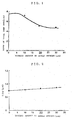
- Fig.1 is a graph showing a relation between an etching amount and a depth of local deep pit of a wafer subjected to alkali etching after lapping.
- Fig.2 is a graph showing a relation between an etching amount and TTV (flatness) of a wafer subjected to alkali etching after lapping.
- Fig.3 is a graph showing a relation between an etching amount and surface roughness (Ra) of a wafer subjected to alkali etching after lapping.
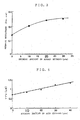
- Fig.4 is a graph showing a relation between an etching amount and TTV (flatness) of a wafer subjected to acid etching after lapping.
- Fig.5 is a graph showing a relation between an etching amount and a generation rate of stain of a wafer subjected to acid etching after lapping.
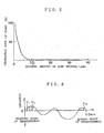
- Fig.6 is an explanatory view of definition of waviness on the surface of the wafer.
- Fig.7 is a view showing results of measurement of power spectrum density by analyzing a frequency of waviness on the back surface of the base wafer (Example 4).
- Curved line A shows a result as for the wafer of Example 1 subjected to both alkali etching and acid etching.
- Curved line B shows a result as for the wafer of Comparative Example 1 subjected to only alkali etching.
- Curved line C shows a result as for the wafer subjected to only acid etching.
- the inventors have studied a base wafer wherein flatness after lapping can be maintained, and particles and contamination are hardly generated, when producing PW for a base wafer for producing a bonded wafer, and have thought out that alkali etching is conducted first in order to remove a distorted layer with maintaining flatness after lapping, then acid etching, especially reaction-controlled acid etching is conducted in order to improve deep pits remaining there, surface roughness or waviness, and subsequently mirror polishing of a chamfered part where particles are apt to be generated is conducted.
- a double-side polished wafer is excellent in flatness, and found that improvement of flatness and reduction of particle generation can be realized at the same time without increasing time for mirror edge polishing, if acid etching is conducted as etching before double-side polishing and a chamfered part is subjected to mirror polishing, and thereby completed the present invention.
- Fig.1 shows a relation between an etching amount and a depth of local deep pit of a wafer having a diameter of 8 inches subjected to lapping with lapping abrasive grains #1200 and then to alkali etching at 85°C with 50% aqueous solution of NaOH.
- Fig.2 shows a relation between etching amount and TTV of the above-mentioned wafer.
- Fig.3 shows a relation between etching amount and surface roughness (Ra).
- the local deep pit means pit that is formed as a result of sticking of lapping abrasive grains on the surface of the wafer during lapping and is increased in size and depth due to alkali etching. If concentration of alkali is low, depth of pit tends to increase. If concentration of alkali is high, depth of pit can be shallow, but in that case, etching amount needs to be large, and therefore, efficiency is low.
- the depth of the pit is measured by the depth of focus of a optical microscope. In order to remove the pits, polishing is necessary in a mirror polishing process, which is the later process. Since stock removal of the mirror polishing needs to be the maximal value of the depth of such a deep pit or more, it is preferable to make pit shallow as possible.
- TTV Total Thickness Vairation
- ⁇ m is a value of difference between thickness of the wafer at the thickest part and thickness of the wafer at the thinnest part in one wafer, and is an index of flatness of the wafer.
- LTV Local Thickness Variation
- LTV of each cell is called LTV cbc
- LTV max the maximal value in one wafer.
- Ra( ⁇ m) is center line average roughness, which is one of surface roughness parameters used most often.
- etching amount of 10 ⁇ m or more in alkali etching is necessary (Fig.1). It is preferable to etch at etching amount of 30 ⁇ m or less in order to achieve TTV (Fig.2) of 1 ⁇ m or less and Ra (Fig.3) of 0.25 ⁇ m or less. Accordingly, considering all of the above-mentioned facts, a suitable range of etching amount in alkali etching is 10 to 30 ⁇ m. Etching amount of about 20 ⁇ m is especially preferable in order to obtain a wafer wherein depth of a local deep pit is close to the minimum value (about 5 ⁇ m), and TTV and Ra are not degraded so much.
- Fig.5 shows a relation between an etching amount of a chemically etched wafer subjected to general acid etching and a generation rate of failure such as spot called stain due to unevenness of etching. Presence or absence of stain generation was determined by observing with naked eye under collimated light.
- an etching amount in acid etching needs to be at least 5 ⁇ m or more. In order to prevent generation of stain surely, an etching amount of 10 ⁇ m or more is necessary. On the other hand, as shown in Fig.4, in order to achieve TTV of one ⁇ m or less, a suitable etching amount is 20 ⁇ m or less. Accordingly, considering all of the above-mentioned facts, a suitable range of an etching amount in acid etching is 5 to 20 ⁇ m, and about 10 ⁇ m is especially preferable.
- an etching amount in alkali etching needs to be larger than an etching amount in acid etching.
- the main reason therefor is as follows. In order to make a depth of local deep pits remaining after alkali etching shallow, the etching amount in alkali etching needs to be large, and it is larger than the etching amount in acid etching necessary to make a rate of stain generation and flatness small.
- the uneven shape at a chamfered part of a base wafer can be made smooth, so that efficiency of mirror polishing at a chamfered part can be improved. More specifically, if time necessary for mirror finishing at a chamfered part (mirror edge polishing) of a wafer subjected to general acid etching only is defined as 1, the time is 2 as for a wafer subjected to alkali etching only, and sometimes it was necessary to grind a chamfered part again before mirror edge polishing in that case. However, in the case of the above-mentioned alkali etching + acid etching, the above-mentioned time is 1.1 to 1.3.
- mirror surface can be obtained with a polishing stock removal of about 1 ⁇ m to several ⁇ m.
- the mirror edge polishing may be conducted before bonding a base wafer to a bond wafer, or after producing a bonded wafer.
- the present invention it is preferable to conduct acid etching after conducting alkali etching and then dipping the wafer in an aqueous solution of hydrogen peroxide. Because, the surface of the wafer after alkali etching is active and hydrophobic, so that impurities are easily adhered thereon, namely the surface is apt to be contaminated. If the surface is made hydrophilic by immersing it in the aqueous solution of hydrogen peroxide to be oxidized, particles are hardly adhered thereon. Accordingly, an acid etching solution used in the next step is never contaminated with particles.
- Preferable concentration of an aqueous solution of hydrogen peroxide is 0.1 to 30 %. Because, the concentration less than 0.1 % is insufficient to make the surface hydrophilic, and 30 % is enough therefor, and higher concentration is economically disadvantageous.
- a solution for reaction-controlled acid etching is an aqueous solution of mixed acids comprising hydrofluoric acid, nitric acid, acetic acid and water in which silicon is dissolved at concentration of 20 to 30 g/l.
- the solution has a relatively similar effect to that of an alkali etching solution.
- the etching solution is called reaction-controlled acid etching. Because, it is acid of which an etching rate is determined depending on a reaction rate, whereas an etching rate is determined depending on a diffusion rate in the case of an aqueous solution of a mixed acid that is a general acid etching solution.
- reaction-controlled acid etching is conducted after alkali etching, a distorted layer due to mechanical working is removed by alkali etching with maintaining flatness after lapping, and then by the reaction-controlled acid etching, local deep pits remaining after alkali etching and unevenness having a sharp shape on the surface can be removed to provide a smooth surface, and surface roughness is improved, and generation of stain can be suppressed. Furthermore, waviness is also suppressed more compared to diffusion-controlled acid etching, so that flatness can be further improved.
- a base wafer can be processed to have an excellent flatness in a large area such that the average value of waviness on the back surface is 0.04 ⁇ m or less.
- waviness component having a wavelength of 10 mm on the back surface is 0.5 to 10 ⁇ m 3 as a power spectrum density.
- the second method only acid etching is conducted as etching of a base wafer, both surface of the etched wafer is polished with a double side polishing apparatus, and a chamfered part is subjected to mirror polishing.
- CW obtained by acid etching is used, a base wafer having excellent flatness can be obtained by conducting double side polishing.
- generation of particles from the back surface can be reduced, since the back surface (the opposite surface to the surface to which a bond wafer is bonded) is also mirror surface. Since unevenness at a chamfered part of the wafer is the same as that of CW obtained by general acid etching, mirror finishing of a chamfered part can also be easily conducted.
- a bonded wafer wherein a back surface and a chamfered part are mirror surface, flatness is excellent, and only few particles are generated.
- mirror edge polishing may be conducted before bonding the base wafer to the bond wafer or after producing a bonded wafer.
- lapped wafer having a diameter of 200 mm lapping abrasive grains No.: #1200
- the following etching treatment was conducted.
- the wafers of which chamfered parts were ground with # 1500 were used.
- alkali etching was conducted with an target etching amount of 20 ⁇ m by immersing the wafer in 50 % by weight aqueous solution of NaOH at 85°C for 450 seconds. Then, treatment for allowing the surface hydrophilic was conducted by immersing the wafer in 0.3 % aqueous solution of hydrogen peroxide, followed by acid etching with an target etching amount of 10 ⁇ m using a mixed acid wherein commercially available 50 % hydrofluoric acid, 70 % nitric acid, and 99 % acetic acid were mixed at a volume rate of 1:2:1. Then, etching effect to the etched wafer (CW) was evaluated by measuring flatness, surface roughness, pit depth and waviness. The results were shown in Table 1.
- TTV flatness measuring apparatus manufactured by ADE corporation
- Ra surface roughness
- Measurement of waviness was conducted by universal surface shape measuring device manufactured by Kosaka Laboratory, Ltd. (SE-3F type).
- the method for measurement comprises tracing 60 mm at a center part on the surface of the wafer (having a diameter of 200 mm) with a probe, and only shape components excluding fine roughness components are measured.
- the waviness is determined as shown in Fig.6. Namely, height at a point where measurement is begun and height at a point where measurement is stopped were equalized, and it is defined as an origin, variation was measured at an interval of 2 mm, and the average Y of the absolute value of the variation Y1 to Y29 was defined as waviness.
- a bond wafer having a diameter of 200 mm wherein a thermal oxide film having a thickness of about 0.5 ⁇ m was formed on the surface, and the mirror surface thereof was bonded to the mirror surface of the above-mentioned base wafer, and then subjected to heat treatment at 1100°C for 2 hours.
- the bond wafer was then subjected to grinding and polishing to produce a bonded SOI wafer having a thickness of 4 ⁇ 0.5 ⁇ m.
- the SOI wafer was processed according to PACE method, until the thickness gets about 100 nm.
- standard deviation ( ⁇ ) of SOI thickness distribution after PACE processing was about 3.2 nm. Accordingly, SOI wafer having sufficient thickness uniformity of 100 ⁇ 10 nm (0.1 ⁇ 0.01 ⁇ m) could be produced.
- Example 1 Using a lapped wafer of same specification as that used in Example 1, a base wafer was produced according to the same method as Example 1 except using a mixed acid in which silicon is previously dissolved at concentration of 27.5 g/1 at acid etching after alkali etching, and was evaluated according to the same method. The results were shown in Table 1.
- the SOI wafer was also produced according to the same method as Example 1. Thickness of the resultant wafer was about 100 nm, and standard deviation ( ⁇ ) of SOI thickness distribution was about 2.5 nm.
- CW was produced by conducting only alkali etching described in Example 1 (target etching amount of 20 ⁇ m) using a lapped wafer of same specification as Example 1, and was evaluated according to the same method. The results were shown in Table 1. A chamfered part of the CW wafer after measurement was subjected to mirror finishing by the same method as Example 1 using a mirror edge polishing apparatus. It took 200 seconds or more to obtain a mirror surface having the same level as Example 1.
- CW was produced by conducting acid etching under the same condition as that of Example 1 with an etching amount of 20 ⁇ m using a lapped wafer of same specification as Example 1 without conducting alkali etching.
- a chamfered part was subjected to mirror finishing by the same method as Example 1 using a mirror edge polishing apparatus. It took about 90 seconds or more to obtain a mirror surface having the same level as Example 1.
- a base wafer was produced by subjecting the CW to double side polishing using a double side polishing apparatus, and SOI wafer was produced using the base wafer by the same method as Example 1.
- the resultant wafer had thickness of about 100 nm and a standard deviation ( ⁇ ) of SOI layer thickness distribution was about 2.0 nm.
- the shape of the back surface of the base wafer of the SOI wafer produced in Example 1 was measured using AutoSort 200 (manufactured by Tropel Corporation, a brand name). Power spectrum density (PSD) was determined by conducting analysis of frequency according to the following manner. The results of the analysis was shown in Fig.7.
- Curved line A shows a result as for the SOI wafer of Example 1
- Curved lines B, C show a result as for a back surface of the wafer of Comparative Example 1 subjected to only alkali etching (CW) and a result as for a back surface of the wafer subjected to only acid etching using a mixed acid consisting of hydrofluoric acid and a nitric acid with 30 ⁇ m instead of alkali etching of Comparative Example 1.
- CW alkali etching
- alkali etching + acid etching of the present invention Fig.7A
- only alkali etching Fig.7B
- only acid etching Fig.7C
- specific power spectrum density of A, B, C in waviness component having a wavelength 10 mm were about 2 ⁇ m 3 , 0.4 ⁇ m 3 , 20 ⁇ m 3 respectively.
- Analysis of frequency in the present example was conducted as follows. First, about 2000 points in the surface of the wafer was measured with AutoSort200 (described above) for measuring a distance from a detector to the back surface of the wafer without contact, and then the measured data was input to a computer, and frequency analysis was conducted, which comprises filter treatment, followed by Fourier transformation to obtain amplitude and calculation of power spectrum density.
- the filter treatment is conducted in order to take basic periodical component that will be necessary for Fourier transformation, there are conducted treatment for finding a center line and treatment for taking out an interval containing data according to Window function.
- F(k) is amplitude at wave number k.
- X i is measured data, i is number of data.
- j represents imaginary number.
- Real number item and imaginary number item in Fourier transformation represent amplitude of sin component and amplitude of cos component.
- the present invention is not limited to the above-described embodiment.
- the above-described embodiment is a mere example, and those having the substantially same structure as that described in the appended claims and providing the similar action and effects are included in the scope of the present invention.
- additives such as surfactants can be added to alkali etching solution and acid etching solution in the above-mentioned embodiments. Specifically, if nitrites such as NaNO 2 is added to the alkali etching solution, there can be achieved an effect of making pits shallow. If surfactants such as fluoro or nonion surfactant is added, an effect of reducing stain can be obtained.
- an aqueous solution of mixed acid comprising hydrofluoric acid, nitric acid, acetic acid and water
- an aqueous solution of mixed acids comprising hydrofluoric acid, nitric acid and water, excluding acetic acid can be used to achieve the similar effect to those of the present invention.
Applications Claiming Priority (3)
| Application Number | Priority Date | Filing Date | Title |
|---|---|---|---|
| JP20158599 | 1999-07-15 | ||
| JP20158599 | 1999-07-15 | ||
| PCT/JP2000/004634 WO2001006564A1 (fr) | 1999-07-15 | 2000-07-11 | Procede de production d'une plaquette encollee et plaquette encollee |
Publications (3)
| Publication Number | Publication Date |
|---|---|
| EP1134808A1 true EP1134808A1 (fr) | 2001-09-19 |
| EP1134808A4 EP1134808A4 (fr) | 2005-10-05 |
| EP1134808B1 EP1134808B1 (fr) | 2011-10-05 |
Family
ID=16443505
Family Applications (1)
| Application Number | Title | Priority Date | Filing Date |
|---|---|---|---|
| EP00944401A Expired - Lifetime EP1134808B1 (fr) | 1999-07-15 | 2000-07-11 | Procede de production d'une plaquette encollee |
Country Status (4)
| Country | Link |
|---|---|
| US (2) | US6716722B1 (fr) |
| EP (1) | EP1134808B1 (fr) |
| KR (1) | KR100701342B1 (fr) |
| WO (1) | WO2001006564A1 (fr) |
Cited By (3)
| Publication number | Priority date | Publication date | Assignee | Title |
|---|---|---|---|---|
| WO2003046994A1 (fr) * | 2001-11-27 | 2003-06-05 | Shin-Etsu Handotai Co., Ltd. | Procede de fabrication d'une tranche collee |
| WO2003046968A1 (fr) * | 2001-11-28 | 2003-06-05 | Shin-Etsu Handotai Co., Ltd. | Procede de production d'une tranche de silicone, tranche de silicone et tranche soi |
| WO2007066886A1 (fr) * | 2005-12-05 | 2007-06-14 | Industry-Academic Cooperation Foundation Gyeongsang National University | Tranche de silicium pour semi-conducteur avec systeme d'alimentation a la face arriere de la tranche |
Families Citing this family (19)
| Publication number | Priority date | Publication date | Assignee | Title |
|---|---|---|---|---|
| KR100420205B1 (ko) * | 2001-09-10 | 2004-03-04 | 주식회사 하이닉스반도체 | 웨이퍼 제조 방법 |
| JP4192482B2 (ja) * | 2002-03-22 | 2008-12-10 | 株式会社Sumco | シリコンウェーハの製造方法 |
| WO2004021420A2 (fr) * | 2002-08-29 | 2004-03-11 | Massachusetts Institute Of Technology | Systeme de fabrication ameliore et procede pour semi-conducteur monocristallin sur un substrat |
| FR2875947B1 (fr) * | 2004-09-30 | 2007-09-07 | Tracit Technologies | Nouvelle structure pour microelectronique et microsysteme et procede de realisation |
| FR2876220B1 (fr) * | 2004-10-06 | 2007-09-28 | Commissariat Energie Atomique | Procede d'elaboration de structures empilees mixtes, a zones isolantes diverses et/ou zones de conduction electrique verticale localisees. |
| EP1667223B1 (fr) * | 2004-11-09 | 2009-01-07 | S.O.I. Tec Silicon on Insulator Technologies S.A. | Méthode de fabrication de plaquettes composites |
| FR2897982B1 (fr) | 2006-02-27 | 2008-07-11 | Tracit Technologies Sa | Procede de fabrication des structures de type partiellement soi, comportant des zones reliant une couche superficielle et un substrat |
| US20080206992A1 (en) * | 2006-12-29 | 2008-08-28 | Siltron Inc. | Method for manufacturing high flatness silicon wafer |
| US8278187B2 (en) * | 2009-06-24 | 2012-10-02 | Semiconductor Energy Laboratory Co., Ltd. | Method for reprocessing semiconductor substrate by stepwise etching with at least two etching treatments |
| KR20120032487A (ko) * | 2009-06-24 | 2012-04-05 | 가부시키가이샤 한도오따이 에네루기 켄큐쇼 | 반도체 기판의 재생 처리 및 soi 기판의 제작 방법 |
| FR2995136B1 (fr) * | 2012-09-04 | 2015-06-26 | Soitec Silicon On Insulator | Pseudo-substrat avec efficacite amelioree d'utilisation d'un materiau monocristallin |
| US8860040B2 (en) | 2012-09-11 | 2014-10-14 | Dow Corning Corporation | High voltage power semiconductor devices on SiC |
| US9018639B2 (en) | 2012-10-26 | 2015-04-28 | Dow Corning Corporation | Flat SiC semiconductor substrate |
| CN103924305B (zh) * | 2013-01-14 | 2017-12-05 | 东莞东阳光科研发有限公司 | 一种准单晶硅片绒面的制备方法 |
| US9797064B2 (en) | 2013-02-05 | 2017-10-24 | Dow Corning Corporation | Method for growing a SiC crystal by vapor deposition onto a seed crystal provided on a support shelf which permits thermal expansion |
| US9738991B2 (en) | 2013-02-05 | 2017-08-22 | Dow Corning Corporation | Method for growing a SiC crystal by vapor deposition onto a seed crystal provided on a supporting shelf which permits thermal expansion |
| US9017804B2 (en) | 2013-02-05 | 2015-04-28 | Dow Corning Corporation | Method to reduce dislocations in SiC crystal growth |
| US8940614B2 (en) | 2013-03-15 | 2015-01-27 | Dow Corning Corporation | SiC substrate with SiC epitaxial film |
| US9279192B2 (en) | 2014-07-29 | 2016-03-08 | Dow Corning Corporation | Method for manufacturing SiC wafer fit for integration with power device manufacturing technology |
Citations (4)
| Publication number | Priority date | Publication date | Assignee | Title |
|---|---|---|---|---|
| US4588473A (en) * | 1982-09-28 | 1986-05-13 | Tokyo Shibaura Denki Kabushiki Kaisha | Semiconductor wafer process |
| EP0460437A2 (fr) * | 1990-05-18 | 1991-12-11 | Fujitsu Limited | Procédé pour fabriquer un substrat semi-conducteur et procédé pour fabriquer un dispositif semi-conducteur comportant ce substrat |
| EP0797248A2 (fr) * | 1996-03-18 | 1997-09-24 | Shin-Etsu Handotai Kabushiki Kaisha | Méthode pour fixer ensemble deux plaquettes semi-conductrices |
| US5899731A (en) * | 1996-09-12 | 1999-05-04 | Komatsu Electronic Metals Co., Ltd. | Method of fabricating a semiconductor wafer |
Family Cites Families (10)
| Publication number | Priority date | Publication date | Assignee | Title |
|---|---|---|---|---|
| JP2565440B2 (ja) | 1991-09-30 | 1996-12-18 | 信越半導体株式会社 | Soi基板の製造方法 |
| JP3449492B2 (ja) | 1993-02-10 | 2003-09-22 | 三菱住友シリコン株式会社 | ウェーハエッチングの前処理方法 |
| JP2910507B2 (ja) * | 1993-06-08 | 1999-06-23 | 信越半導体株式会社 | 半導体ウエーハの製造方法 |
| JP2875722B2 (ja) | 1993-10-05 | 1999-03-31 | 三菱マテリアルシリコン株式会社 | 半導体ウェーハのエッチング処理装置 |
| JPH08107091A (ja) * | 1994-09-30 | 1996-04-23 | Kyushu Komatsu Denshi Kk | Soi基板の製法 |
| US5932048A (en) * | 1995-04-06 | 1999-08-03 | Komatsu Electronic Metals Co., Ltd. | Method of fabricating direct-bonded semiconductor wafers |
| JP3480480B2 (ja) * | 1996-03-06 | 2003-12-22 | 三菱住友シリコン株式会社 | Soi基板の製造方法 |
| JP3305610B2 (ja) | 1997-02-21 | 2002-07-24 | 信越半導体株式会社 | ラッピング後の半導体ウエーハの洗浄方法 |
| JPH10335195A (ja) * | 1997-05-27 | 1998-12-18 | Mitsubishi Materials Shilicon Corp | 張り合わせ基板の製造方法 |
| JP3686910B2 (ja) * | 1997-09-29 | 2005-08-24 | 三菱住友シリコン株式会社 | シリコンウェーハのエッチング方法 |
-
2000
- 2000-07-11 KR KR1020017003265A patent/KR100701342B1/ko active IP Right Grant
- 2000-07-11 EP EP00944401A patent/EP1134808B1/fr not_active Expired - Lifetime
- 2000-07-11 US US09/787,038 patent/US6716722B1/en not_active Expired - Lifetime
- 2000-07-11 WO PCT/JP2000/004634 patent/WO2001006564A1/fr active Application Filing
-
2003
- 2003-10-23 US US10/690,541 patent/US20040081805A1/en not_active Abandoned
Patent Citations (4)
| Publication number | Priority date | Publication date | Assignee | Title |
|---|---|---|---|---|
| US4588473A (en) * | 1982-09-28 | 1986-05-13 | Tokyo Shibaura Denki Kabushiki Kaisha | Semiconductor wafer process |
| EP0460437A2 (fr) * | 1990-05-18 | 1991-12-11 | Fujitsu Limited | Procédé pour fabriquer un substrat semi-conducteur et procédé pour fabriquer un dispositif semi-conducteur comportant ce substrat |
| EP0797248A2 (fr) * | 1996-03-18 | 1997-09-24 | Shin-Etsu Handotai Kabushiki Kaisha | Méthode pour fixer ensemble deux plaquettes semi-conductrices |
| US5899731A (en) * | 1996-09-12 | 1999-05-04 | Komatsu Electronic Metals Co., Ltd. | Method of fabricating a semiconductor wafer |
Non-Patent Citations (2)
| Title |
|---|
| MITANI K ET AL: "CONTRIBUTION OF POLISHED SURFACE WAVENESS TO FINAL SOI THICKNESS UNIFORMITY OF BONDED WAFERS THROUGH PACE PROCESS" IEICE TRANSACTIONS ON ELECTRONICS, INSTITUTE OF ELECTRONICS INFORMATION AND COMM. ENG. TOKYO, JP, vol. E80-C, no. 3, March 1997 (1997-03), pages 370-377, XP000949876 ISSN: 0916-8524 * |
| See also references of WO0106564A1 * |
Cited By (9)
| Publication number | Priority date | Publication date | Assignee | Title |
|---|---|---|---|---|
| WO2003046994A1 (fr) * | 2001-11-27 | 2003-06-05 | Shin-Etsu Handotai Co., Ltd. | Procede de fabrication d'une tranche collee |
| EP1460691A1 (fr) * | 2001-11-27 | 2004-09-22 | Shin-Etsu Handotai Co., Ltd | Procede de fabrication d'une tranche collee |
| EP1460691A4 (fr) * | 2001-11-27 | 2005-12-14 | Shinetsu Handotai Kk | Procede de fabrication d'une tranche collee |
| CN1326247C (zh) * | 2001-11-27 | 2007-07-11 | 信越半导体株式会社 | 贴合晶片的制造方法 |
| US7531425B2 (en) | 2001-11-27 | 2009-05-12 | Shin-Etsu Handotai Co., Ltd. | Method of fabricating bonded wafer |
| WO2003046968A1 (fr) * | 2001-11-28 | 2003-06-05 | Shin-Etsu Handotai Co., Ltd. | Procede de production d'une tranche de silicone, tranche de silicone et tranche soi |
| WO2007066886A1 (fr) * | 2005-12-05 | 2007-06-14 | Industry-Academic Cooperation Foundation Gyeongsang National University | Tranche de silicium pour semi-conducteur avec systeme d'alimentation a la face arriere de la tranche |
| US7915725B2 (en) | 2005-12-05 | 2011-03-29 | Industry-Academic Cooperation Foundation Gyeongsang National University | Silicon wafer for semiconductor with powersupply system on the backside of wafer |
| US8242590B2 (en) | 2005-12-05 | 2012-08-14 | Industry-Academic Cooperation Foundation Gyeongsang National University | Silicon wafer for semiconductor with powersupply system on the backside of wafer |
Also Published As
| Publication number | Publication date |
|---|---|
| US6716722B1 (en) | 2004-04-06 |
| KR100701342B1 (ko) | 2007-03-29 |
| WO2001006564A1 (fr) | 2001-01-25 |
| US20040081805A1 (en) | 2004-04-29 |
| KR20010075093A (ko) | 2001-08-09 |
| EP1134808A4 (fr) | 2005-10-05 |
| EP1134808B1 (fr) | 2011-10-05 |
Similar Documents
| Publication | Publication Date | Title |
|---|---|---|
| US6716722B1 (en) | Method of producing a bonded wafer and the bonded wafer | |
| US6884696B2 (en) | Method for producing bonding wafer | |
| EP1962325B1 (fr) | Procédé de fabrication d'un substrat lié | |
| US7855129B2 (en) | Method for manufacturing direct bonded SOI wafer and direct bonded SOI wafer manufactured by the method | |
| US8772875B2 (en) | Semiconductor on glass substrate with stiffening layer | |
| US7790565B2 (en) | Semiconductor on glass insulator made using improved thinning process | |
| EP1189266B1 (fr) | Procede d'obtention de tranches de silicium ou de soi et tranches ainsi obtenues | |
| TWI394204B (zh) | 鍵合晶圓的製造方法 | |
| KR100972213B1 (ko) | Soi 웨이퍼의 제조 방법 및 soi 웨이퍼 | |
| EP0928017B1 (fr) | Procédé de production des plaquettes semi-conductrices | |
| US7312154B2 (en) | Method of polishing a semiconductor-on-insulator structure | |
| JP2006222453A (ja) | シリコンウエーハの製造方法及びシリコンウエーハ並びにsoiウエーハ | |
| US20090061593A1 (en) | Semiconductor Wafer Re-Use in an Exfoliation Process Using Heat Treatment | |
| KR20030089712A (ko) | Soi 웨이퍼 및 그 제조방법 | |
| EP2261954A1 (fr) | Procede de fabrication d'un substrat silicium sur isolant | |
| JP4855254B2 (ja) | 両面を有するドナーウェハから半導体材料の薄層を形成するための方法 | |
| TWI251875B (en) | Manufacturing method of bonding wafer | |
| EP1548822A1 (fr) | Procede de fabrication de plaquette silicium sur isolant | |
| JP2001085648A (ja) | 貼り合わせウエーハの製造方法および貼り合わせウエーハ | |
| JP5368000B2 (ja) | Soi基板の製造方法 | |
| CN117672813A (zh) | 一种硅片的制备方法及硅片 | |
| JP3951814B2 (ja) | Soi基板の製造方法 |
Legal Events
| Date | Code | Title | Description |
|---|---|---|---|
| PUAI | Public reference made under article 153(3) epc to a published international application that has entered the european phase |
Free format text: ORIGINAL CODE: 0009012 |
|
| 17P | Request for examination filed |
Effective date: 20010328 |
|
| AK | Designated contracting states |
Kind code of ref document: A1 Designated state(s): AT BE CH CY DE DK ES FI FR GB GR IE IT LI LU MC NL PT SE |
|
| AX | Request for extension of the european patent |
Free format text: AL;LT;LV;MK;RO;SI |
|
| RBV | Designated contracting states (corrected) |
Designated state(s): DE FR GB |
|
| A4 | Supplementary search report drawn up and despatched |
Effective date: 20050824 |
|
| 17Q | First examination report despatched |
Effective date: 20090128 |
|
| RAP1 | Party data changed (applicant data changed or rights of an application transferred) |
Owner name: SHIN-ETSU HANDOTAI CO., LTD. |
|
| RTI1 | Title (correction) |
Free format text: A METHOD OF PRODUCING A BONDED WAFER |
|
| GRAP | Despatch of communication of intention to grant a patent |
Free format text: ORIGINAL CODE: EPIDOSNIGR1 |
|
| GRAS | Grant fee paid |
Free format text: ORIGINAL CODE: EPIDOSNIGR3 |
|
| GRAA | (expected) grant |
Free format text: ORIGINAL CODE: 0009210 |
|
| AK | Designated contracting states |
Kind code of ref document: B1 Designated state(s): DE FR GB |
|
| REG | Reference to a national code |
Ref country code: GB Ref legal event code: FG4D |
|
| REG | Reference to a national code |
Ref country code: DE Ref legal event code: R096 Ref document number: 60046515 Country of ref document: DE Effective date: 20111208 |
|
| PLBE | No opposition filed within time limit |
Free format text: ORIGINAL CODE: 0009261 |
|
| STAA | Information on the status of an ep patent application or granted ep patent |
Free format text: STATUS: NO OPPOSITION FILED WITHIN TIME LIMIT |
|
| 26N | No opposition filed |
Effective date: 20120706 |
|
| REG | Reference to a national code |
Ref country code: DE Ref legal event code: R097 Ref document number: 60046515 Country of ref document: DE Effective date: 20120706 |
|
| GBPC | Gb: european patent ceased through non-payment of renewal fee |
Effective date: 20120711 |
|
| PG25 | Lapsed in a contracting state [announced via postgrant information from national office to epo] |
Ref country code: GB Free format text: LAPSE BECAUSE OF NON-PAYMENT OF DUE FEES Effective date: 20120711 |
|
| REG | Reference to a national code |
Ref country code: FR Ref legal event code: PLFP Year of fee payment: 17 |
|
| REG | Reference to a national code |
Ref country code: FR Ref legal event code: PLFP Year of fee payment: 18 |
|
| REG | Reference to a national code |
Ref country code: FR Ref legal event code: PLFP Year of fee payment: 19 |
|
| PGFP | Annual fee paid to national office [announced via postgrant information from national office to epo] |
Ref country code: FR Payment date: 20190619 Year of fee payment: 20 |
|
| PGFP | Annual fee paid to national office [announced via postgrant information from national office to epo] |
Ref country code: DE Payment date: 20190625 Year of fee payment: 20 |
|
| REG | Reference to a national code |
Ref country code: DE Ref legal event code: R071 Ref document number: 60046515 Country of ref document: DE |