EP1133086A2 - Polarization mode dispersion measurement using phase-sensitive sideband detection - Google Patents
Polarization mode dispersion measurement using phase-sensitive sideband detection Download PDFInfo
- Publication number
- EP1133086A2 EP1133086A2 EP01301718A EP01301718A EP1133086A2 EP 1133086 A2 EP1133086 A2 EP 1133086A2 EP 01301718 A EP01301718 A EP 01301718A EP 01301718 A EP01301718 A EP 01301718A EP 1133086 A2 EP1133086 A2 EP 1133086A2
- Authority
- EP
- European Patent Office
- Prior art keywords
- signal
- phase
- output
- optical
- sideband
- Prior art date
- Legal status (The legal status is an assumption and is not a legal conclusion. Google has not performed a legal analysis and makes no representation as to the accuracy of the status listed.)
- Granted
Links
- 230000010287 polarization Effects 0.000 title claims abstract description 53
- 239000006185 dispersion Substances 0.000 title claims abstract description 30
- 238000005259 measurement Methods 0.000 title claims abstract description 4
- 238000001514 detection method Methods 0.000 title abstract description 5
- 230000003287 optical effect Effects 0.000 claims abstract description 44
- 230000005540 biological transmission Effects 0.000 claims description 7
- 239000013307 optical fiber Substances 0.000 abstract description 10
- 230000001902 propagating effect Effects 0.000 abstract description 2
- 239000000835 fiber Substances 0.000 description 6
- 238000000034 method Methods 0.000 description 5
- 230000009268 pathologic speech processing Effects 0.000 description 5
- 208000032207 progressive 1 supranuclear palsy Diseases 0.000 description 5
- 238000010586 diagram Methods 0.000 description 4
- 238000004891 communication Methods 0.000 description 3
- 230000010363 phase shift Effects 0.000 description 3
- 239000011159 matrix material Substances 0.000 description 2
- 238000012986 modification Methods 0.000 description 2
- 230000004048 modification Effects 0.000 description 2
- 230000004044 response Effects 0.000 description 2
- 238000011896 sensitive detection Methods 0.000 description 2
- 230000018199 S phase Effects 0.000 description 1
- 238000004364 calculation method Methods 0.000 description 1
- 230000008859 change Effects 0.000 description 1
- 238000006243 chemical reaction Methods 0.000 description 1
- 238000012937 correction Methods 0.000 description 1
- 230000008878 coupling Effects 0.000 description 1
- 238000010168 coupling process Methods 0.000 description 1
- 238000005859 coupling reaction Methods 0.000 description 1
- 230000001419 dependent effect Effects 0.000 description 1
- 238000010291 electrical method Methods 0.000 description 1
- 238000010237 hybrid technique Methods 0.000 description 1
- 238000000691 measurement method Methods 0.000 description 1
- 238000005457 optimization Methods 0.000 description 1
- 230000008569 process Effects 0.000 description 1
- 238000011084 recovery Methods 0.000 description 1
- 230000035945 sensitivity Effects 0.000 description 1
- 230000008054 signal transmission Effects 0.000 description 1
- 238000001228 spectrum Methods 0.000 description 1
- 238000012360 testing method Methods 0.000 description 1
Images


Classifications
-
- H—ELECTRICITY
- H04—ELECTRIC COMMUNICATION TECHNIQUE
- H04B—TRANSMISSION
- H04B10/00—Transmission systems employing electromagnetic waves other than radio-waves, e.g. infrared, visible or ultraviolet light, or employing corpuscular radiation, e.g. quantum communication
- H04B10/25—Arrangements specific to fibre transmission
- H04B10/2507—Arrangements specific to fibre transmission for the reduction or elimination of distortion or dispersion
- H04B10/2569—Arrangements specific to fibre transmission for the reduction or elimination of distortion or dispersion due to polarisation mode dispersion [PMD]
Definitions
- the present invention relates to an optical communication system and, more particularly, to the utilization of a phase-sensitive detection arrangement on each sideband of a double sideband signal to measure polarization mode dispersion (PMD).
- PMD polarization mode dispersion
- Polarization mode dispersion occurs in an optical fiber as a result of a small residual birefringence that is introduced in the fiber core by asymmetric internal stress or strain, as well as random polarization coupling due to external forces acting upon the fiber. Consequently, PMD may severely impair the transmission of a signal in an optical fiber-based network.
- PSP principal states of polarization
- the output will consist of both PSPs, with a certain amount of delay (in time) between them. It is this differential group delay (DGD) that causes waveform distortion.
- DTD differential group delay
- PMD polarization mode dispersion
- the distorted optical signal is first converted to an electrical signal at the receiver.
- a delay line filter with specific weights is then used to partially compensate for the distortion due to PMD.
- An exemplary hybrid technique may utilize a polarization controller and a section of polarization maintaining fiber.
- a high-speed photo-detector is used to convert the optical signal into an electrical representation.
- An electrical tapped delay line filter is then used to adjust the frequency-dependent phase of the electrical signal.
- the widely-used modulation phase shift technique utilizes a double-sideband modulated signal and a swept carrier frequency to measure delay.
- the sidebands are required to exhibit the same amplitude and the change in delay and frequency must be accurately measured to obtain the dispersion parameter.
- a need remaining in the prior art is addressed by the present invention, which relates to an optical communication system and, more particularly, to the utilization of a phase-sensitive detection arrangement on each sideband of a double sideband signal to measure polarization mode dispersion (PMD).
- PMD polarization mode dispersion
- single-sideband self-homodyne signals are generated (or detected) and each sideband is separately processed to determine delay and dispersion information.
- information on both principal states of polarization can be collected and then used to determine the polarization mode dispersion.
- a narrowband optical filter is used to generate a signal including upper and lower sideband components from the received (and polarized) optical signal.
- the output form the narrowband filter is then used as an input to a phase-sensitive single sideband detector circuit which includes an RF signal generator, multipliers and phase shifter to form both in-phase and quadrature outputs.
- the magnitudes and phase of the output are used to form the dispersion information.
- the narrowband optical filter includes a half-wave plate at its input and is used to process both polarizations of the optical signal, eliminating any discrepancies in the processed magnitude and phase information for each polarization.
- phase-sensitive sideband detection on an optical signal propagating through a dispersive element, such as an optical fiber
- information can be collected regarding polarization mode dispersion (PMD) and this information used to correct/compensate for this dispersion.
- PMD polarization mode dispersion
- the Taylor series expansion of the phase is given by: ⁇ (f m ) - ⁇ (0) ⁇ -2 ⁇ m - ⁇ 2 ⁇ m 2 D/c, where in this expansion the odd function yields the relative delay ⁇ and the even function yields the chromatic dispersion D (in ps/nm).
- ⁇ o ( ⁇ USB - ⁇ LSB )/2, which characterizes the delay ⁇ . Therefore, a single modulation frequency (f m ) can be used to provide the dispersion and delay information, eliminating the need to "sweep" the center frequency, as used in prior art arrangements.
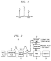
- FIG. 2 illustrates an exemplary optical communication system 10 that may employ the phase-sensitive single sideband PMD measurement technique of the present invention.
- a data signal d n is impressed upon an optical transmitter 12 and is thereafter communicated through a dispersive element 14, in this case, an optical fiber.
- a dispersive element 14 in this case, an optical fiber.
- the polarization mode dispersion introduced by fiber 14 is measured in accordance with the present invention and an appropriate compensation is introduced into the optical signal.
- an optical tap 16 is used to remove a portion of the signal experiencing PMD from the transmission path, where the tapped-off portion is applied as an input to an exemplary PMD measuring arrangement 18, formed in accordance with the present invention and described in more detail below.
- a polarization mode dispersion compensator 22 is then used to introduce the desired amount of compensation so as to produce an optical output signal with minimal dispersion.
- the compensated signal may be applied as an input to an optical receiver 24 (as shown), or any other appropriate optical element (for example, an optical amplifier).
- FIG. 3 illustrates transmitter 12 and optical fiber 14, as discussed above, in association with the particular elements comprising PMD measuring arrangement 18 as taught by this invention.
- the output signal from optical fiber 14 is first passed through a polarization beam splitter 30, which separates the optical signal into the two orthogonal principal states of polarization, allowing for polarization dispersion to be properly measured.
- a first polarization state, defined as u, is then characterized within a first single sideband phase-sensitive detector 32.
- the remaining, orthogonal polarization v is similarly characterized within a second single sideband phase-sensitive detector 34.
- the PMD of optical fiber 14 can be described by the Jones matrix: where u(f) ⁇ U(f)exp[j ⁇ u (f)] and v(f) ⁇ V(f)exp[j ⁇ v(f)].
- Detector 34 comprises an optical filter 40 that is coupled to the output of polarization beam splitter 30 and used to generate/detect the separate sideband signals that are used to determine the delay and dispersion characteristics of the received signal.
- a particular detected sideband signal is subsequently transferred into the electrical domain by a photodetector 42 and passed through an RF modulator arrangement 44, as shown, to determine the in-phase and quadrature magnitude and phase components.
- RF modulator arrangement 44 comprises an RF reference source 46 (which may be associated with, for example, a local clock at a receiver, a local oscillator, or any suitable RF reference source).
- the RF signal having a predetermined frequency (defined as f m ) is passed through a 90° phase shift element 48 and applied as a first input to multiplier 50, the remaining input being the electrical output from photodetector 42, the multiplier output forming the quadrature component of the received sideband signal. Thereafter, the quadrature component is passed through a low pass filter 52 and an A/D converter 54 to generate a first output component, denoted "y" in FIG. 4, and defined as the magnitude of the quadrature component of the processed sideband signal.
- the RF signal is also applied as an input to a second multiplier 56, the remaining input being also the output from photodetector 42, the output of second multiplier 56 being the in-phase component of the received single sideband signal.
- the in-phase component is also passed through a low pass filter 58 and subjected to a conversion in A/D converter 60 to form the second output component, denoted "x" in FIG. 4 and defined as the magnitude of the in-phase component.
- measuring tones may be impressed on the data signal (or any appropriate "test" data signal sent through the transmission system and recovered as the sideband signals used for the PMD measuring purposes of the present invention.
- the data-loaded signal itself may be employed to generate the sideband signals (at the receiver) using a set of optical narrowband filters so that no modifications are required at the transmit end.
- FIG. 5 illustrates an exemplary narrowband filter arrangement 40 that may be interposed between the output of polarization beam splitter 30 and each phase-sensitive detector.
- narrowband filter arrangement 40 comprises an integrated planar waveguide ring resonator circuit including three separate ring resonators 72, 74 and 76.
- thermo-optic phase shifter denoted 78, 80 and 82.
- a set of optical couplers 84 disposed at the outputs of each ring resonator, are configured in a compact manner to generate and combine the sidebands and carrier frequency. The sidebands are measured simultaneously, resulting in the ability to provide information quickly with little sensitivity to changes in the data spectrum or path length.
- the resonance of central ring 74 can be locked by dithering the ring's phase shifter 80 to optimize the detector carrier-frequency power.
- the resonances of sideband rings 72 and 76 are locked by optimizing the detected power at the local oscillator frequency.
- the same optical filter 40 may be used to provide phase detection for the orthogonal polarization output from beam splitter 30, as indicated by the dotted arrows and coupler shown in phantom in FIG. 5.
- a pair of balanced detectors 88 and 90 at the output of center ring 74 may be measured to determine the phase difference between the orthogonal polarizations, ⁇ (0), at the carrier frequency, as required for the calculation of the principal states of polarization from the estimated Jones matrix.
- Phase-sensitive detectors 92 and 94 (configured as discussed above in association with FIG. 4) provide the magnitude and phase information for the USB and LSB sidebands, respectively, while phase-sensitive detectors 96, 98 are used in conjunction with the center frequency component to provide the amplitude of the orthogonal polarizations.
- the sum of the sideband components characterize the dispersion present in the optical signal and the difference of the sideband components characterize the delay.
Landscapes
- Physics & Mathematics (AREA)
- Electromagnetism (AREA)
- Engineering & Computer Science (AREA)
- Computer Networks & Wireless Communication (AREA)
- Signal Processing (AREA)
- Optical Communication System (AREA)
- Investigating Or Analysing Materials By Optical Means (AREA)
Abstract
Description

Claims (10)
- In an optical transmission system, a polarization mode dispersion measuring arrangement comprisinga polarization beam splitter responsive to a tapped-off portion of an optical signal for dividing the signal into first and second orthogonally polarized signals;a narrowband filter, responsive separately to the first and second orthogonal signals, for generating therefrom a center frequency component, an upper sideband signal component and a lower sideband signal component for both said first and second orthogonal signals;a first phase-sensitive single sideband detector circuit, responsive to the components generated by the narrowband filter for the first orthogonally polarized signal and producing as an output magnitude and phase information for said first orthogonally polarized signal; anda second phase-sensitive single sideband detector circuit, responsive to the components generated by the narrowband filter for the second orthogonally polarized signal and producing as an output magnitude and phase information for said second orthogonally polarized signal, the combination of the outputs from the first and second phase-sensitive single sideband detector circuit forming the polarization mode dispersion measurement output of the arrangement.
- The system as defined in claim 1 wherein each phase-sensitive single sideband detector circuit comprisesa photodetector for converting the received optical signal into an electrical signal representation;an RF signal generator;a 90° phase shifter disposed at the output of the RF signal generator;a first multiplier, responsive at its separate inputs to the electrical signal output of the photodetector and the output of the 90° phase shifter, the output of the first multiplier being a quadrature component of the received signal;a first A/D converter, disposed at the output of the first multiplier, to generate a digital signal representation of the magnitude of the quadrature component, denoted as "y";a second multiplier, responsive at its separate inputs to the electrical signal output of the photodetector and the output of the RF signal generator, the output of the second multiplier being an in-phase component of the received signal;a second A/D converter, disposed at the output of the second multiplier, to generate a digital signal representation of the magnitude of the in-phase component, denoted as "x", wherein the phase of the processed optical signal is defined by the relation = tan-1 (y/x).
- The system as defined in claim 2 wherein each single sideband phase-sensitive detector circuit further comprisesa first low pass filter disposed between the first multiplier and the first A/D converter; anda second low pass filter disposed between the second multiplier and the second A/D converter.
- The system as defined in claim 2 wherein the RF signal generator comprises a local oscillator.
- The system as defined in claim 2 wherein the RF signal generator utilizes a recovered clock signal.
- The system as defined in claim 1 wherein the narrowband optical filter comprisesa ring resonator structure including a set of three ring resonators, a first ring resonator for generating the center frequency component, a second ring resonator for generating the upper sideband component, and a third ring resonator for generating the lower sideband component, each ring resonator including a phase shifting element;a plurality of optical couplers for combining the outputs of the set of three ring resonators to form the upper sideband, lower sideband and center frequency outputs of the narrowband filter.
- The system as defined in claim 6 wherein the plurality of optical couplers comprisesa first 2x1 optical coupler responsive to the outputs of the first and second ring resonators for forming the upper sideband output component; anda second 2x1 optical coupler responsive to the outputs of the first and third ring resonators for forming the lower sideband output component.
- The system as defined in claim 6 wherein the narrowband optical filter further comprises a half-wave plate disposed at the input to the set of three ring resonators such that said narrowband optical filter can be used to generate the signal components for both the first and second orthogonally polarized signals.
- The system as defined in claim 8 wherein the set of optical couplers further comprises a 2x2 for receiving as inputs the center frequency components of the first and second orthogonally polarized signals.
- The system as defined in claim 9 wherein the optical filter further comprises a balanced detector for determining the phase difference between the center frequency components of the first and second orthogonally polarized optical signals.
Applications Claiming Priority (4)
| Application Number | Priority Date | Filing Date | Title |
|---|---|---|---|
| US18763000P | 2000-03-08 | 2000-03-08 | |
| US187630P | 2000-03-08 | ||
| US779392 | 2001-02-08 | ||
| US09/779,392 US6362874B1 (en) | 2000-03-08 | 2001-02-08 | Polarization mode dispersion measurement using phase-sensitive sideband detection |
Publications (3)
| Publication Number | Publication Date |
|---|---|
| EP1133086A2 true EP1133086A2 (en) | 2001-09-12 |
| EP1133086A3 EP1133086A3 (en) | 2003-11-12 |
| EP1133086B1 EP1133086B1 (en) | 2007-10-31 |
Family
ID=26883229
Family Applications (1)
| Application Number | Title | Priority Date | Filing Date |
|---|---|---|---|
| EP01301718A Expired - Lifetime EP1133086B1 (en) | 2000-03-08 | 2001-02-26 | Polarization mode dispersion measurement using phase-sensitive sideband detection |
Country Status (4)
| Country | Link |
|---|---|
| US (1) | US6362874B1 (en) |
| EP (1) | EP1133086B1 (en) |
| JP (1) | JP3848843B2 (en) |
| DE (1) | DE60131112T2 (en) |
Cited By (2)
| Publication number | Priority date | Publication date | Assignee | Title |
|---|---|---|---|---|
| GB2380342A (en) * | 2001-09-28 | 2003-04-02 | Fujitsu Network Comm Inc | A compensator for polarisation-mode dispersion (PMD) compensation |
| WO2014048112A1 (en) * | 2012-09-27 | 2014-04-03 | 华为技术有限公司 | Method, device and system for measuring parameter of optical communication medium |
Families Citing this family (19)
| Publication number | Priority date | Publication date | Assignee | Title |
|---|---|---|---|---|
| JP4004720B2 (en) * | 2000-08-09 | 2007-11-07 | 富士通株式会社 | Chromatic dispersion measuring apparatus and method |
| US7536108B2 (en) * | 2001-06-29 | 2009-05-19 | Nippon Telegraph & Telephone Corporation | High precision chromatic dispersion measuring method and automatic dispersion compensating optical link system that uses this method |
| US7035538B2 (en) * | 2001-07-09 | 2006-04-25 | University Of Southern California | Monitoring optical dispersion based on vestigial side band optical filtering |
| JP3880360B2 (en) * | 2001-10-12 | 2007-02-14 | 株式会社アドバンテスト | Polarization mode dispersion measuring apparatus, method, and recording medium |
| US20030099423A1 (en) * | 2001-11-29 | 2003-05-29 | Koorosh Aflatooni | Planar lightwave circuit having an integrated dispersion compensator using a fourier filter |
| US7206516B2 (en) * | 2002-04-30 | 2007-04-17 | Pivotal Decisions Llc | Apparatus and method for measuring the dispersion of a fiber span |
| US6894780B2 (en) * | 2002-06-18 | 2005-05-17 | Agilent Technologies, Inc. | Pilot tone multiplexing of polarization states in heterodyne optical component analysis |
| US6862377B2 (en) * | 2002-10-15 | 2005-03-01 | Agilent Technologies, Inc. | System and method for PMD measurement from coherent spectral analysis |
| US20040156038A1 (en) * | 2003-02-12 | 2004-08-12 | Xiang-Dong Cao | Method and apparatus for providing real-time chromatic dispersion measurement |
| DE10310015B4 (en) * | 2003-02-28 | 2006-07-06 | Fraunhofer-Gesellschaft zur Förderung der angewandten Forschung e.V. | Opto-electric phase-locked loop for recovering the clock signal in a digital optical transmission system |
| US7375680B2 (en) * | 2005-05-12 | 2008-05-20 | L-3 Communications Corporation | Ionosphere delay measurement using carrier phase |
| US7809284B2 (en) * | 2006-06-23 | 2010-10-05 | Alcatel-Lucent Usa Inc. | System and method for receiving coherent, polarization-multiplexed optical signals |
| CN101682424B (en) | 2007-04-05 | 2014-02-19 | 爱斯福公司 | Method and system for determining in-band optical noise |
| US8364034B2 (en) * | 2007-04-05 | 2013-01-29 | Exfo Inc. | In-band optical noise measurement using differential polarization response |
| WO2009062237A1 (en) * | 2007-11-12 | 2009-05-22 | Nicta Ipr Pty Ltd | In-band osnr monitor with pmd insensitivity |
| US20120170929A1 (en) * | 2011-01-03 | 2012-07-05 | Chongjin Xie | Apparatus And Method For Monitoring An Optical Coherent Network |
| CN105606343B (en) * | 2016-01-28 | 2018-07-24 | 南京航空航天大学 | A kind of Larger Dynamic range optical device measurement method and measuring system |
| CN114323589B (en) * | 2021-12-30 | 2024-08-06 | 苏州六幺四信息科技有限责任公司 | A method and device for fast frequency response measurement of optical devices based on optical double-sideband modulation |
| CN117713695A (en) * | 2022-09-06 | 2024-03-15 | 清华大学 | Signal detection method and system |
Family Cites Families (4)
| Publication number | Priority date | Publication date | Assignee | Title |
|---|---|---|---|---|
| US5949560A (en) * | 1997-02-05 | 1999-09-07 | Northern Telecom Limited | Optical transmission system |
| US6271952B1 (en) * | 1998-08-18 | 2001-08-07 | Nortel Networks Limited | Polarization mode dispersion compensation |
| US6130766A (en) * | 1999-01-07 | 2000-10-10 | Qtera Corporation | Polarization mode dispersion compensation via an automatic tracking of a principal state of polarization |
| US6211957B1 (en) * | 2000-03-03 | 2001-04-03 | Lucent Technologies, Inc. | In-line all-fiber polarimeter |
-
2001
- 2001-02-08 US US09/779,392 patent/US6362874B1/en not_active Expired - Lifetime
- 2001-02-26 EP EP01301718A patent/EP1133086B1/en not_active Expired - Lifetime
- 2001-02-26 DE DE60131112T patent/DE60131112T2/en not_active Expired - Lifetime
- 2001-03-08 JP JP2001064305A patent/JP3848843B2/en not_active Expired - Fee Related
Cited By (4)
| Publication number | Priority date | Publication date | Assignee | Title |
|---|---|---|---|---|
| GB2380342A (en) * | 2001-09-28 | 2003-04-02 | Fujitsu Network Comm Inc | A compensator for polarisation-mode dispersion (PMD) compensation |
| GB2380342B (en) * | 2001-09-28 | 2005-08-10 | Fujitsu Network Comm Inc | A compensator for polarisation-mode dispersion compensation |
| US7218800B2 (en) | 2001-09-28 | 2007-05-15 | Fujitsu Limited | Compensator for polarization-mode dispersion compensation |
| WO2014048112A1 (en) * | 2012-09-27 | 2014-04-03 | 华为技术有限公司 | Method, device and system for measuring parameter of optical communication medium |
Also Published As
| Publication number | Publication date |
|---|---|
| DE60131112D1 (en) | 2007-12-13 |
| EP1133086B1 (en) | 2007-10-31 |
| EP1133086A3 (en) | 2003-11-12 |
| DE60131112T2 (en) | 2008-08-07 |
| US6362874B1 (en) | 2002-03-26 |
| JP3848843B2 (en) | 2006-11-22 |
| JP2001296207A (en) | 2001-10-26 |
Similar Documents
| Publication | Publication Date | Title |
|---|---|---|
| US6362874B1 (en) | Polarization mode dispersion measurement using phase-sensitive sideband detection | |
| US8406621B2 (en) | Method and apparatus for measuring a factor characterizing a balanced detection device | |
| US6130766A (en) | Polarization mode dispersion compensation via an automatic tracking of a principal state of polarization | |
| EP2672636B1 (en) | Coherent optical receiver, and inter-channel skew detection device and detection method in coherent optical receiver | |
| US6807321B2 (en) | Apparatus and method for measurement and adaptive control of polarization mode dispersion in optical fiber transmission systems | |
| US8229254B2 (en) | Systems and methods for polarization mode dispersion mitigation | |
| CN105794129B (en) | Polarization Independent Coherent Optical Receivers | |
| CN101167273A (en) | Method and device for in-band optical performance monitoring | |
| US20060098989A1 (en) | System for minimizing or compensating pmd-induced distortion in optical transmission systems and transmission fibres in particular | |
| CN117882317B (en) | Detection device, light receiving device, optical communication system, storage medium and detection method | |
| US20020018213A1 (en) | Wavelength dispersion measuring device and a method thereof | |
| CA2280578C (en) | Polarisation mode dispersion measurement | |
| US7075659B2 (en) | Heterodyne optical network analysis that utilizes signal modulation | |
| JP2019161246A (en) | Digital coherent transmission system | |
| WO2002066940A2 (en) | System and method for measurement of the state of polarization of an optical signal in a fibre | |
| CN119522545B (en) | Control device, compensation device, program, and control method | |
| Eyal et al. | Polarization dependence of the intensity modulation transfer function of an optical system with PMD and PDL | |
| Madsen | Chromatic and polarization mode dispersion measurement technique using phase-sensitive sideband detection | |
| JP3379473B2 (en) | Dispersion measuring device | |
| Westlund et al. | Novel technique for polarization independent all-optical sampling in fiber |
Legal Events
| Date | Code | Title | Description |
|---|---|---|---|
| PUAI | Public reference made under article 153(3) epc to a published international application that has entered the european phase |
Free format text: ORIGINAL CODE: 0009012 |
|
| AK | Designated contracting states |
Kind code of ref document: A2 Designated state(s): AT BE CH CY DE DK ES FI FR GB GR IE IT LI LU MC NL PT SE TR |
|
| AX | Request for extension of the european patent |
Free format text: AL;LT;LV;MK;RO;SI |
|
| PUAL | Search report despatched |
Free format text: ORIGINAL CODE: 0009013 |
|
| AK | Designated contracting states |
Kind code of ref document: A3 Designated state(s): AT BE CH CY DE DK ES FI FR GB GR IE IT LI LU MC NL PT SE TR |
|
| AX | Request for extension of the european patent |
Extension state: AL LT LV MK RO SI |
|
| 17P | Request for examination filed |
Effective date: 20040504 |
|
| AKX | Designation fees paid |
Designated state(s): AT BE CH CY DE DK ES FI FR GB GR IE IT LI LU MC NL PT SE TR |
|
| 17Q | First examination report despatched |
Effective date: 20060828 |
|
| GRAP | Despatch of communication of intention to grant a patent |
Free format text: ORIGINAL CODE: EPIDOSNIGR1 |
|
| RBV | Designated contracting states (corrected) |
Designated state(s): DE FR GB |
|
| GRAS | Grant fee paid |
Free format text: ORIGINAL CODE: EPIDOSNIGR3 |
|
| GRAA | (expected) grant |
Free format text: ORIGINAL CODE: 0009210 |
|
| AK | Designated contracting states |
Kind code of ref document: B1 Designated state(s): DE FR GB |
|
| REG | Reference to a national code |
Ref country code: GB Ref legal event code: FG4D |
|
| REF | Corresponds to: |
Ref document number: 60131112 Country of ref document: DE Date of ref document: 20071213 Kind code of ref document: P |
|
| ET | Fr: translation filed | ||
| PLBE | No opposition filed within time limit |
Free format text: ORIGINAL CODE: 0009261 |
|
| STAA | Information on the status of an ep patent application or granted ep patent |
Free format text: STATUS: NO OPPOSITION FILED WITHIN TIME LIMIT |
|
| 26N | No opposition filed |
Effective date: 20080801 |
|
| REG | Reference to a national code |
Ref country code: GB Ref legal event code: 732E Free format text: REGISTERED BETWEEN 20131031 AND 20131106 |
|
| REG | Reference to a national code |
Ref country code: FR Ref legal event code: CD Owner name: ALCATEL-LUCENT USA INC. Effective date: 20131122 |
|
| REG | Reference to a national code |
Ref country code: FR Ref legal event code: GC Effective date: 20140410 |
|
| REG | Reference to a national code |
Ref country code: FR Ref legal event code: RG Effective date: 20141015 |
|
| REG | Reference to a national code |
Ref country code: FR Ref legal event code: PLFP Year of fee payment: 15 |
|
| REG | Reference to a national code |
Ref country code: FR Ref legal event code: PLFP Year of fee payment: 16 |
|
| PGFP | Annual fee paid to national office [announced via postgrant information from national office to epo] |
Ref country code: DE Payment date: 20160218 Year of fee payment: 16 |
|
| PGFP | Annual fee paid to national office [announced via postgrant information from national office to epo] |
Ref country code: FR Payment date: 20160218 Year of fee payment: 16 Ref country code: GB Payment date: 20160217 Year of fee payment: 16 |
|
| REG | Reference to a national code |
Ref country code: DE Ref legal event code: R119 Ref document number: 60131112 Country of ref document: DE |
|
| GBPC | Gb: european patent ceased through non-payment of renewal fee |
Effective date: 20170226 |
|
| REG | Reference to a national code |
Ref country code: FR Ref legal event code: ST Effective date: 20171031 |
|
| PG25 | Lapsed in a contracting state [announced via postgrant information from national office to epo] |
Ref country code: DE Free format text: LAPSE BECAUSE OF NON-PAYMENT OF DUE FEES Effective date: 20170901 Ref country code: FR Free format text: LAPSE BECAUSE OF NON-PAYMENT OF DUE FEES Effective date: 20170228 |
|
| PG25 | Lapsed in a contracting state [announced via postgrant information from national office to epo] |
Ref country code: GB Free format text: LAPSE BECAUSE OF NON-PAYMENT OF DUE FEES Effective date: 20170226 |