EP1132494A2 - Deposition and annealing of multicomponent ZrSnTi and HfSnTi oxide thin films using solventless liquid mixture of precursors - Google Patents
Deposition and annealing of multicomponent ZrSnTi and HfSnTi oxide thin films using solventless liquid mixture of precursors Download PDFInfo
- Publication number
- EP1132494A2 EP1132494A2 EP01105786A EP01105786A EP1132494A2 EP 1132494 A2 EP1132494 A2 EP 1132494A2 EP 01105786 A EP01105786 A EP 01105786A EP 01105786 A EP01105786 A EP 01105786A EP 1132494 A2 EP1132494 A2 EP 1132494A2
- Authority
- EP
- European Patent Office
- Prior art keywords
- approximately
- mixtures
- metal
- films
- annealing
- Prior art date
- Legal status (The legal status is an assumption and is not a legal conclusion. Google has not performed a legal analysis and makes no representation as to the accuracy of the status listed.)
- Granted
Links
- 239000000203 mixture Substances 0.000 title claims abstract description 60
- 239000002243 precursor Substances 0.000 title claims abstract description 47
- 239000007788 liquid Substances 0.000 title claims abstract description 42
- 239000010409 thin film Substances 0.000 title claims abstract description 32
- 238000000137 annealing Methods 0.000 title claims abstract description 16
- 230000008021 deposition Effects 0.000 title claims description 23
- 229910052751 metal Inorganic materials 0.000 claims abstract description 51
- 239000002184 metal Substances 0.000 claims abstract description 51
- 239000010408 film Substances 0.000 claims abstract description 43
- 238000000034 method Methods 0.000 claims abstract description 31
- 238000000151 deposition Methods 0.000 claims description 30
- 238000006243 chemical reaction Methods 0.000 claims description 24
- GQPLMRYTRLFLPF-UHFFFAOYSA-N Nitrous Oxide Chemical compound [O-][N+]#N GQPLMRYTRLFLPF-UHFFFAOYSA-N 0.000 claims description 20
- QVGXLLKOCUKJST-UHFFFAOYSA-N atomic oxygen Chemical compound [O] QVGXLLKOCUKJST-UHFFFAOYSA-N 0.000 claims description 14
- 239000001301 oxygen Substances 0.000 claims description 14
- 229910052760 oxygen Inorganic materials 0.000 claims description 14
- MHAJPDPJQMAIIY-UHFFFAOYSA-N Hydrogen peroxide Chemical compound OO MHAJPDPJQMAIIY-UHFFFAOYSA-N 0.000 claims description 13
- 239000000758 substrate Substances 0.000 claims description 13
- 229910052734 helium Inorganic materials 0.000 claims description 12
- 239000000376 reactant Substances 0.000 claims description 12
- 239000007789 gas Substances 0.000 claims description 10
- 229910001868 water Inorganic materials 0.000 claims description 10
- XLYOFNOQVPJJNP-UHFFFAOYSA-N water Substances O XLYOFNOQVPJJNP-UHFFFAOYSA-N 0.000 claims description 8
- 229910052726 zirconium Inorganic materials 0.000 claims description 8
- MWUXSHHQAYIFBG-UHFFFAOYSA-N Nitric oxide Chemical compound O=[N] MWUXSHHQAYIFBG-UHFFFAOYSA-N 0.000 claims description 6
- 150000004703 alkoxides Chemical class 0.000 claims description 6
- 229910052735 hafnium Inorganic materials 0.000 claims description 6
- 238000003860 storage Methods 0.000 claims description 6
- 150000001408 amides Chemical class 0.000 claims description 5
- 125000000217 alkyl group Chemical group 0.000 claims description 4
- 239000003990 capacitor Substances 0.000 claims description 4
- MGWGWNFMUOTEHG-UHFFFAOYSA-N 4-(3,5-dimethylphenyl)-1,3-thiazol-2-amine Chemical compound CC1=CC(C)=CC(C=2N=C(N)SC=2)=C1 MGWGWNFMUOTEHG-UHFFFAOYSA-N 0.000 claims description 3
- PXGOKWXKJXAPGV-UHFFFAOYSA-N Fluorine Chemical compound FF PXGOKWXKJXAPGV-UHFFFAOYSA-N 0.000 claims description 3
- CBENFWSGALASAD-UHFFFAOYSA-N Ozone Chemical compound [O-][O+]=O CBENFWSGALASAD-UHFFFAOYSA-N 0.000 claims description 3
- 239000003570 air Substances 0.000 claims description 3
- 150000001540 azides Chemical class 0.000 claims description 3
- 125000002915 carbonyl group Chemical group [*:2]C([*:1])=O 0.000 claims description 3
- 150000007942 carboxylates Chemical class 0.000 claims description 3
- 125000000058 cyclopentadienyl group Chemical group C1(=CC=CC1)* 0.000 claims description 3
- 229910052731 fluorine Inorganic materials 0.000 claims description 3
- 239000011737 fluorine Substances 0.000 claims description 3
- 150000003949 imides Chemical class 0.000 claims description 3
- JCXJVPUVTGWSNB-UHFFFAOYSA-N nitrogen dioxide Inorganic materials O=[N]=O JCXJVPUVTGWSNB-UHFFFAOYSA-N 0.000 claims description 3
- 239000001272 nitrous oxide Substances 0.000 claims description 3
- 230000005855 radiation Effects 0.000 claims description 3
- 150000007944 thiolates Chemical class 0.000 claims description 3
- 125000004169 (C1-C6) alkyl group Chemical group 0.000 claims description 2
- 229910019142 PO4 Inorganic materials 0.000 claims description 2
- 150000004820 halides Chemical class 0.000 claims description 2
- 150000004678 hydrides Chemical class 0.000 claims description 2
- 150000002823 nitrates Chemical class 0.000 claims description 2
- 235000021317 phosphate Nutrition 0.000 claims description 2
- 150000003013 phosphoric acid derivatives Chemical class 0.000 claims description 2
- 125000000547 substituted alkyl group Chemical group 0.000 claims description 2
- 239000002904 solvent Substances 0.000 abstract description 18
- 238000002347 injection Methods 0.000 abstract description 8
- 239000007924 injection Substances 0.000 abstract description 8
- 150000002739 metals Chemical class 0.000 abstract description 8
- RTAQQCXQSZGOHL-UHFFFAOYSA-N Titanium Chemical compound [Ti] RTAQQCXQSZGOHL-UHFFFAOYSA-N 0.000 abstract description 5
- XNFDWBSCUUZWCI-UHFFFAOYSA-N [Zr].[Sn] Chemical compound [Zr].[Sn] XNFDWBSCUUZWCI-UHFFFAOYSA-N 0.000 abstract description 3
- 239000003054 catalyst Substances 0.000 abstract description 3
- PRGGQOPNRRRVIO-UHFFFAOYSA-N [Hf].[Sn] Chemical compound [Hf].[Sn] PRGGQOPNRRRVIO-UHFFFAOYSA-N 0.000 abstract description 2
- 239000000443 aerosol Substances 0.000 abstract description 2
- 230000004888 barrier function Effects 0.000 abstract description 2
- 239000003989 dielectric material Substances 0.000 abstract description 2
- 238000004519 manufacturing process Methods 0.000 abstract description 2
- 239000002887 superconductor Substances 0.000 abstract description 2
- 238000004377 microelectronic Methods 0.000 abstract 1
- 239000011253 protective coating Substances 0.000 abstract 1
- 238000005229 chemical vapour deposition Methods 0.000 description 37
- 239000003446 ligand Substances 0.000 description 18
- SDTMFDGELKWGFT-UHFFFAOYSA-N 2-methylpropan-2-olate Chemical compound CC(C)(C)[O-] SDTMFDGELKWGFT-UHFFFAOYSA-N 0.000 description 9
- 239000000463 material Substances 0.000 description 8
- 150000002736 metal compounds Chemical class 0.000 description 7
- 239000007787 solid Substances 0.000 description 6
- 239000001307 helium Substances 0.000 description 5
- SWQJXJOGLNCZEY-UHFFFAOYSA-N helium atom Chemical compound [He] SWQJXJOGLNCZEY-UHFFFAOYSA-N 0.000 description 5
- 229910044991 metal oxide Inorganic materials 0.000 description 5
- 150000004706 metal oxides Chemical class 0.000 description 5
- 238000012545 processing Methods 0.000 description 5
- 150000001875 compounds Chemical class 0.000 description 4
- 239000012705 liquid precursor Substances 0.000 description 4
- 238000005259 measurement Methods 0.000 description 4
- 239000000126 substance Substances 0.000 description 4
- 238000009834 vaporization Methods 0.000 description 4
- 230000008016 vaporization Effects 0.000 description 4
- 238000004458 analytical method Methods 0.000 description 3
- 238000003877 atomic layer epitaxy Methods 0.000 description 3
- 229910052454 barium strontium titanate Inorganic materials 0.000 description 3
- 150000004696 coordination complex Chemical class 0.000 description 3
- 239000010410 layer Substances 0.000 description 3
- 238000002488 metal-organic chemical vapour deposition Methods 0.000 description 3
- 229910003455 mixed metal oxide Inorganic materials 0.000 description 3
- 238000005240 physical vapour deposition Methods 0.000 description 3
- 239000004065 semiconductor Substances 0.000 description 3
- 239000000243 solution Substances 0.000 description 3
- 229910052718 tin Inorganic materials 0.000 description 3
- 229910052719 titanium Inorganic materials 0.000 description 3
- GWEVSGVZZGPLCZ-UHFFFAOYSA-N titanium dioxide Inorganic materials O=[Ti]=O GWEVSGVZZGPLCZ-UHFFFAOYSA-N 0.000 description 3
- 229910052788 barium Inorganic materials 0.000 description 2
- 239000003153 chemical reaction reagent Substances 0.000 description 2
- 238000005260 corrosion Methods 0.000 description 2
- 230000007797 corrosion Effects 0.000 description 2
- 229910001338 liquidmetal Inorganic materials 0.000 description 2
- 239000012299 nitrogen atmosphere Substances 0.000 description 2
- 238000005001 rutherford backscattering spectroscopy Methods 0.000 description 2
- 238000003980 solgel method Methods 0.000 description 2
- 239000011877 solvent mixture Substances 0.000 description 2
- 229910052712 strontium Inorganic materials 0.000 description 2
- PBCFLUZVCVVTBY-UHFFFAOYSA-N tantalum pentoxide Inorganic materials O=[Ta](=O)O[Ta](=O)=O PBCFLUZVCVVTBY-UHFFFAOYSA-N 0.000 description 2
- 238000007669 thermal treatment Methods 0.000 description 2
- OYPRJOBELJOOCE-UHFFFAOYSA-N Calcium Chemical compound [Ca] OYPRJOBELJOOCE-UHFFFAOYSA-N 0.000 description 1
- 229910007991 Si-N Inorganic materials 0.000 description 1
- 229910006294 Si—N Inorganic materials 0.000 description 1
- 229910008839 Sn—Ti Inorganic materials 0.000 description 1
- ATJFFYVFTNAWJD-UHFFFAOYSA-N Tin Chemical compound [Sn] ATJFFYVFTNAWJD-UHFFFAOYSA-N 0.000 description 1
- -1 Transition-Metal Nitride Chemical class 0.000 description 1
- 239000002253 acid Substances 0.000 description 1
- 230000002411 adverse Effects 0.000 description 1
- 239000003513 alkali Substances 0.000 description 1
- 229910052784 alkaline earth metal Inorganic materials 0.000 description 1
- 150000001342 alkaline earth metals Chemical class 0.000 description 1
- 238000005275 alloying Methods 0.000 description 1
- 238000013459 approach Methods 0.000 description 1
- DSAJWYNOEDNPEQ-UHFFFAOYSA-N barium atom Chemical compound [Ba] DSAJWYNOEDNPEQ-UHFFFAOYSA-N 0.000 description 1
- 230000015572 biosynthetic process Effects 0.000 description 1
- 230000005587 bubbling Effects 0.000 description 1
- 229910052791 calcium Inorganic materials 0.000 description 1
- 239000011575 calcium Substances 0.000 description 1
- 239000012159 carrier gas Substances 0.000 description 1
- 235000019994 cava Nutrition 0.000 description 1
- 239000000919 ceramic Substances 0.000 description 1
- 238000012512 characterization method Methods 0.000 description 1
- 239000011248 coating agent Substances 0.000 description 1
- 238000000576 coating method Methods 0.000 description 1
- 230000000536 complexating effect Effects 0.000 description 1
- 238000009833 condensation Methods 0.000 description 1
- 230000005494 condensation Effects 0.000 description 1
- 239000000470 constituent Substances 0.000 description 1
- 238000011109 contamination Methods 0.000 description 1
- 230000003247 decreasing effect Effects 0.000 description 1
- 239000007857 degradation product Substances 0.000 description 1
- 238000002716 delivery method Methods 0.000 description 1
- 238000005137 deposition process Methods 0.000 description 1
- 238000009792 diffusion process Methods 0.000 description 1
- 230000000694 effects Effects 0.000 description 1
- 238000005441 electronic device fabrication Methods 0.000 description 1
- 239000012776 electronic material Substances 0.000 description 1
- 238000005516 engineering process Methods 0.000 description 1
- 230000007613 environmental effect Effects 0.000 description 1
- 238000011156 evaluation Methods 0.000 description 1
- 230000008020 evaporation Effects 0.000 description 1
- 238000001704 evaporation Methods 0.000 description 1
- 238000010438 heat treatment Methods 0.000 description 1
- 239000011346 highly viscous material Substances 0.000 description 1
- 238000011835 investigation Methods 0.000 description 1
- 238000000608 laser ablation Methods 0.000 description 1
- 239000007791 liquid phase Substances 0.000 description 1
- 229910001507 metal halide Inorganic materials 0.000 description 1
- 150000005309 metal halides Chemical class 0.000 description 1
- 229910052987 metal hydride Inorganic materials 0.000 description 1
- 150000004681 metal hydrides Chemical class 0.000 description 1
- 229910021645 metal ion Inorganic materials 0.000 description 1
- 229910001960 metal nitrate Inorganic materials 0.000 description 1
- 229910001463 metal phosphate Inorganic materials 0.000 description 1
- 238000001465 metallisation Methods 0.000 description 1
- 239000003595 mist Substances 0.000 description 1
- 238000002156 mixing Methods 0.000 description 1
- 238000001451 molecular beam epitaxy Methods 0.000 description 1
- QJGQUHMNIGDVPM-UHFFFAOYSA-N nitrogen group Chemical group [N] QJGQUHMNIGDVPM-UHFFFAOYSA-N 0.000 description 1
- 239000003960 organic solvent Substances 0.000 description 1
- 239000007800 oxidant agent Substances 0.000 description 1
- 230000001590 oxidative effect Effects 0.000 description 1
- 230000000704 physical effect Effects 0.000 description 1
- 238000000053 physical method Methods 0.000 description 1
- 239000002244 precipitate Substances 0.000 description 1
- 238000001556 precipitation Methods 0.000 description 1
- 238000005546 reactive sputtering Methods 0.000 description 1
- 238000005389 semiconductor device fabrication Methods 0.000 description 1
- 239000002356 single layer Substances 0.000 description 1
- 238000004528 spin coating Methods 0.000 description 1
- 238000004544 sputter deposition Methods 0.000 description 1
- CIOAGBVUUVVLOB-UHFFFAOYSA-N strontium atom Chemical compound [Sr] CIOAGBVUUVVLOB-UHFFFAOYSA-N 0.000 description 1
- 125000001424 substituent group Chemical group 0.000 description 1
- 238000006467 substitution reaction Methods 0.000 description 1
- 238000002230 thermal chemical vapour deposition Methods 0.000 description 1
- 238000000427 thin-film deposition Methods 0.000 description 1
- 229910052723 transition metal Inorganic materials 0.000 description 1
Images
Classifications
-
- C—CHEMISTRY; METALLURGY
- C23—COATING METALLIC MATERIAL; COATING MATERIAL WITH METALLIC MATERIAL; CHEMICAL SURFACE TREATMENT; DIFFUSION TREATMENT OF METALLIC MATERIAL; COATING BY VACUUM EVAPORATION, BY SPUTTERING, BY ION IMPLANTATION OR BY CHEMICAL VAPOUR DEPOSITION, IN GENERAL; INHIBITING CORROSION OF METALLIC MATERIAL OR INCRUSTATION IN GENERAL
- C23C—COATING METALLIC MATERIAL; COATING MATERIAL WITH METALLIC MATERIAL; SURFACE TREATMENT OF METALLIC MATERIAL BY DIFFUSION INTO THE SURFACE, BY CHEMICAL CONVERSION OR SUBSTITUTION; COATING BY VACUUM EVAPORATION, BY SPUTTERING, BY ION IMPLANTATION OR BY CHEMICAL VAPOUR DEPOSITION, IN GENERAL
- C23C16/00—Chemical coating by decomposition of gaseous compounds, without leaving reaction products of surface material in the coating, i.e. chemical vapour deposition [CVD] processes
- C23C16/22—Chemical coating by decomposition of gaseous compounds, without leaving reaction products of surface material in the coating, i.e. chemical vapour deposition [CVD] processes characterised by the deposition of inorganic material, other than metallic material
-
- C—CHEMISTRY; METALLURGY
- C23—COATING METALLIC MATERIAL; COATING MATERIAL WITH METALLIC MATERIAL; CHEMICAL SURFACE TREATMENT; DIFFUSION TREATMENT OF METALLIC MATERIAL; COATING BY VACUUM EVAPORATION, BY SPUTTERING, BY ION IMPLANTATION OR BY CHEMICAL VAPOUR DEPOSITION, IN GENERAL; INHIBITING CORROSION OF METALLIC MATERIAL OR INCRUSTATION IN GENERAL
- C23C—COATING METALLIC MATERIAL; COATING MATERIAL WITH METALLIC MATERIAL; SURFACE TREATMENT OF METALLIC MATERIAL BY DIFFUSION INTO THE SURFACE, BY CHEMICAL CONVERSION OR SUBSTITUTION; COATING BY VACUUM EVAPORATION, BY SPUTTERING, BY ION IMPLANTATION OR BY CHEMICAL VAPOUR DEPOSITION, IN GENERAL
- C23C16/00—Chemical coating by decomposition of gaseous compounds, without leaving reaction products of surface material in the coating, i.e. chemical vapour deposition [CVD] processes
- C23C16/44—Chemical coating by decomposition of gaseous compounds, without leaving reaction products of surface material in the coating, i.e. chemical vapour deposition [CVD] processes characterised by the method of coating
- C23C16/448—Chemical coating by decomposition of gaseous compounds, without leaving reaction products of surface material in the coating, i.e. chemical vapour deposition [CVD] processes characterised by the method of coating characterised by the method used for generating reactive gas streams, e.g. by evaporation or sublimation of precursor materials
- C23C16/4481—Chemical coating by decomposition of gaseous compounds, without leaving reaction products of surface material in the coating, i.e. chemical vapour deposition [CVD] processes characterised by the method of coating characterised by the method used for generating reactive gas streams, e.g. by evaporation or sublimation of precursor materials by evaporation using carrier gas in contact with the source material
-
- C—CHEMISTRY; METALLURGY
- C23—COATING METALLIC MATERIAL; COATING MATERIAL WITH METALLIC MATERIAL; CHEMICAL SURFACE TREATMENT; DIFFUSION TREATMENT OF METALLIC MATERIAL; COATING BY VACUUM EVAPORATION, BY SPUTTERING, BY ION IMPLANTATION OR BY CHEMICAL VAPOUR DEPOSITION, IN GENERAL; INHIBITING CORROSION OF METALLIC MATERIAL OR INCRUSTATION IN GENERAL
- C23C—COATING METALLIC MATERIAL; COATING MATERIAL WITH METALLIC MATERIAL; SURFACE TREATMENT OF METALLIC MATERIAL BY DIFFUSION INTO THE SURFACE, BY CHEMICAL CONVERSION OR SUBSTITUTION; COATING BY VACUUM EVAPORATION, BY SPUTTERING, BY ION IMPLANTATION OR BY CHEMICAL VAPOUR DEPOSITION, IN GENERAL
- C23C16/00—Chemical coating by decomposition of gaseous compounds, without leaving reaction products of surface material in the coating, i.e. chemical vapour deposition [CVD] processes
- C23C16/22—Chemical coating by decomposition of gaseous compounds, without leaving reaction products of surface material in the coating, i.e. chemical vapour deposition [CVD] processes characterised by the deposition of inorganic material, other than metallic material
- C23C16/30—Deposition of compounds, mixtures or solid solutions, e.g. borides, carbides, nitrides
- C23C16/40—Oxides
Definitions
- the semiconductor fabrication industry requires materials and deposition technology adequate to deposit metals, metal mixtures and metal compound mixtures in thin layers, plugs, vias and patterns on semiconductor and insulating or dielectric substrates to make appropriate electrical devices for integrated circuits, memory devices and flat panel display devices.
- Various techniques are known for depositing metals, metal compounds and their mixtures on appropriate electronic materials substrates, including; physical methods (sputtering, molecular beam epitaxy, evaporation and laser ablation), alloying, and chemical vapor deposition (plasma, photo or laser enhanced, low pressure and high temperature).
- Chemical vapor deposition has gained favor in recent years due to its properties of providing uniform and conformal deposition and its ability to deposit an array of materials under highly controllable conditions. Typically, chemical vapor deposition can provide high deposition rates of high purity materials in a controlled fashion.
- the situation for chemical vapor deposition is further complicated by the need to co-deposit several chemicals, such as multiple metal oxide chemical vapor deposition. It is possible for metal precursors to react with one another or for at least one metal precursor for CVD to be too volatile or too involatile, i.e., a solid.
- the prior art has used solvents to dissolve solid metal precursors or blend liquid, particularly viscous liquid, metal precursors for CVD.
- US Patent 5,204,314 discloses a foraminous device for flash vaporization of liquid mixtures or solvent mixtures of metal precursors for CVD.
- US Patent 5,820,664 describes various solvent mixtures of mixed metal compound precursors, which are useful for CVD.
- solvent systems for liquid delivery for CVD are problematic because compatible, volatile solvents must be chosen. Solvents decrease the amount of effective reagent that is delivered to the CVD reactor for a given flow and time period. More importantly, solvents introduce yet another reagent into the sensitive reaction zone where delicate semiconductor and electronic device fabrication is being performed. The adverse effects of such solvent presence must be considered. Finally, solvents represent an environmental and cost factor. The solvent or its degradation products must be recycled, captured or treated subsequent to utilization.
- the present invention overcomes these drawbacks by using a solventless, common ligand mixture of metals in a liquid state for deposition preferably by direct liquid injection to avoid solvent and ligand exchange drawbacks for consistent deposition performance, with subsequent annealing to improve electrical properties of the deposited films.
- the appropriate reaction conditions of elevated temperature are approximately 150-600 °C. More preferably, the appropriate reaction conditions of elevated temperature are approximately 200-500°C.
- the solventless liquid mixture is introduced into the reaction zone and vaporized at a temperature of approximately 50-200°C. More preferably, the temperature is approximately 80-120°C.
- the reaction zone pressure is approximately 0.01-50 Torr. More preferably, the pressure is approximately 0.1-5 Torr.
- the deposition rate of the thin film is in the range of approximately 1 to 300 angstoms per minute.
- the oxygen containing reactant is selected from the group of oxygen, ozone, nitrous oxide, nitric oxide, nitrogen dioxide, water, hydrogen peroxide, air and mixtures thereof.
- an anneal gas selected from the group consisting of N 2 , Ar, He, O 2 , O 3 , N 2 O, NO, H 2 O, H 2 O 2 and mixtures of thereof
- the annealing is conducted for a time in the range of 5-30 min.
- the annealing is performed at a temperature in the range of approximately 350-450°C.
- the thin film of XSnTi oxides are deposited as a storage capacitor in a dynamic random access memory device.
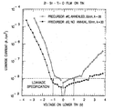
- FIG 1 is a graph of IV (current-voltage) of a Zr-Sn-Ti-Ox (zirconium tin titanate or ZTT) film of the present invention before and after anneal per Example 4.
- Multicomponent metal containing materials such as mixed-metal oxides
- Mixed-metal oxides often have unique physical properties that each individual metal oxide component does not possess.
- some mixed metal oxides can be used for high dielectric constant materials, ferroelectrics, high temperature superconductors, catalysts, and corrosion resistant coating.
- PVD physical vapor deposition
- DLI is particularly a preferred method for the delivery of multi-components because it delivers the same ratio of constituents to the reactor as are in the source container. DLI has the added advantage of storing the precursor at room temperature and heating only the amount required to be delivered, and therefore, improving precursor shelf life.
- volatile components are chosen such that:
- Liquid mixtures can be prepared either by directly mixing liquid metal complexes or dissolving solid metal complex(es) in liquid metal complex(es). In these systems, no solvent is needed to dissolve or dilute the precursor mixtures to achieve a total liquid phase of the resulting mixtures.
- a broad range of MOCVD precursor solutions using organic solvents have previously been claimed as precursors for thin film depositions.
- Our new non-solvent containing precursor mixtures lower the burden of abatement of the CVD effluent in the exhaust because there is no extra volatile organic medium to be collected after the CVD processing. Besides, since no solvent is used in the liquid mixtures described herein, high throughput of metal containing vapor can be delivered into the CVD reactor.
- the multi-component precursors are selected from the group consisting of, but not limited to, metal alkyls, metal alkoxides, metal halides, metal hydrides, metal amides, metal, imides, metal azides, metal cyclopentadienyls, metal carbonyls, metal nitrates, metal thiolates, metal carboxylates, metal phosphates, metal ⁇ -diketonates, metal ⁇ -ketoiminates, and metal ⁇ -diiminates, and their fluorine and other substituted analogs and mixtures thereof.
- the ligand associated with each metal should be the same to avoid ligand exchanges which might result in non-liquid conditions.
- oxygen containing reactant oxidant
- the oxygen containing reactant can be selected from the group of oxygen, ozone, nitrous oxide, nitric oxide, nitrogen dioxide, water, hydrogen peroxide, air and mixtures thereof.
- the above precursors could be used for plasma, photo, or laser enhanced CVD deposition, well recognized deposition techniques, or by atomic layer epitaxy.
- atomic layer epitaxy an approximately single layer of precursor molecules are first adsorbed on a surface. A reactant is then dosed onto this first precursor layer followed by a reaction between the reactant and the first precursor already on the surface. This alternating procedure is then repeated to provide the desired thickness of element or compound in a near atomic thickness layer.
- liquid mixture precursors may also be applied to sol-gel processing and spin coating of films.
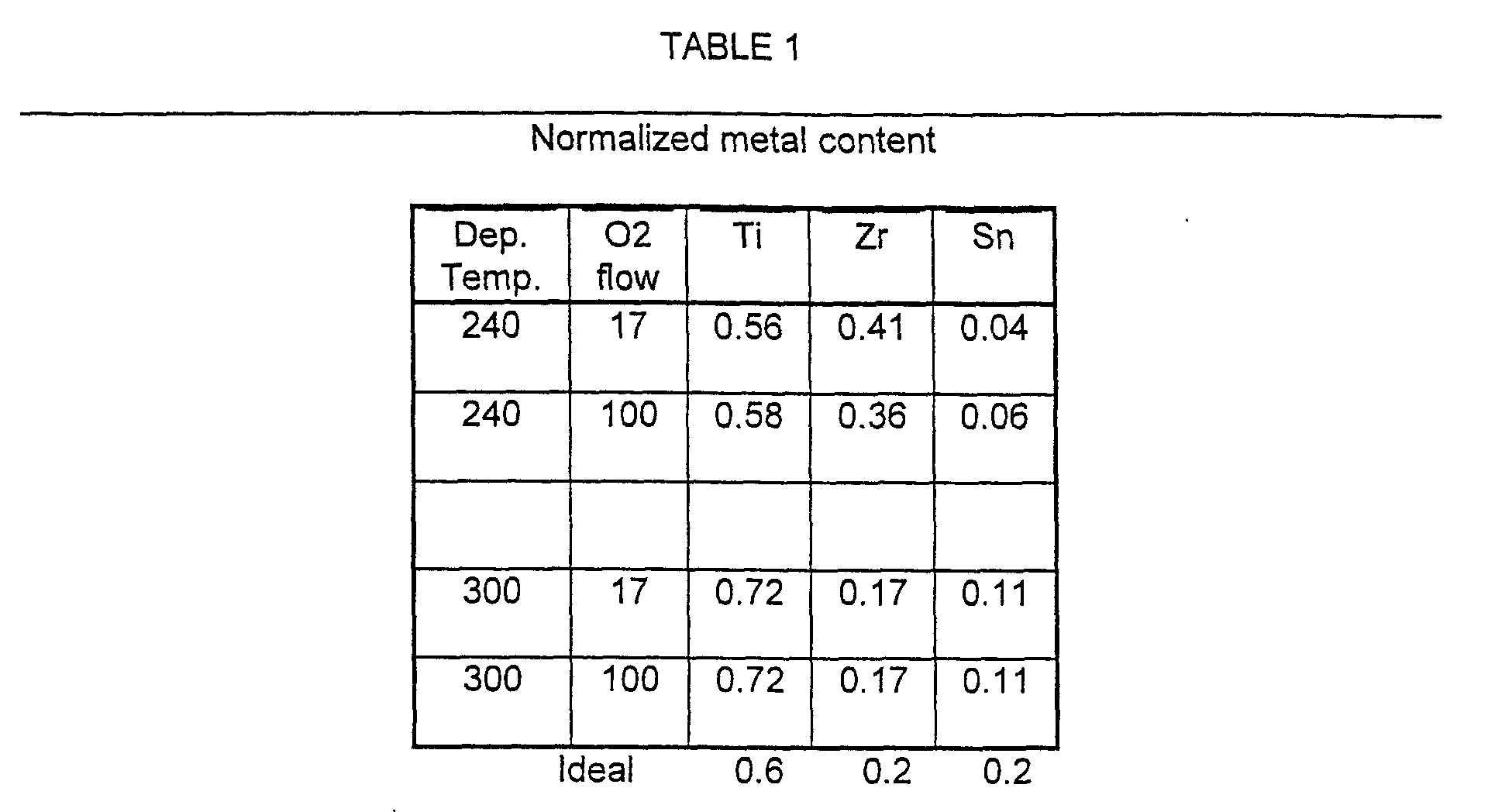
- the ratio of Zr:Sn:Ti 0.1-0.3:0.1-0.3:0.4-0.8.
- HfSnTi 0.05-0.30:0.01-0.20:0.50 - 0.94.
- Appropriate reaction conditions of elevated temperature are approximately 150-600 °C. More preferably, the appropriate reaction conditions of elevated temperature are approximately 200-500°C.
- the solventless liquid mixture may be introduced into the reaction zone and vaporized at a temperature of approximately 50-200°C. More preferably, the temperature is approximately 80-120°C.
- the reaction zone pressure may be approximately 0.01-50 Torr. More preferably, the pressure is approximately 0.1 -5 Torr.
- the deposition rate of the thin film is in the range of approximately 1 to 300 angstoms per minute.
- the films are annealed at a temperature in the range of approximately 200-500°C, in an anneal gas selected from the group consisting of N 2 , Ar, He, O 2 , O 3 , N 2 O, NO, H 2 O, H 2 O 2 and mixtures of thereof for 1 to 60 minutes to improve their electrical properties as shown in FIG 1.
- Annealed films are compared against non-annealed films, wherein the annealed films show consistently lower leakage current rates required of materials in electronic structures.
- the films are annealed under N 2 atmosphere at 400°C for 30min.
- Such films can be used as storage capacitors for dynamic random access memory devices.
- Example 1 CVD of ZrSnTiOx from metal amides
- the deposition rate ranged from 100 to 300 angstroms per minute.
- the reactor chamber pressure was 2 Torr.
- the deposition rate ranged from 20 to 80 angstroms per minute.
- the reactor chamber pressure was 2 Torr.
- EDX Energy dispersive X-ray
- Example 3 thermal anneal of ZrSnTiOx thin films deposited from metal alkoxides
- the dielelectric constant of the films increased to 38 after the anneal.
- Example 4 leakage current of ZrSnTiOx thin films deposited from metal alkoxides
- TiN bottom electrode and Ag top electrode were used for the I-V (current-voltage) measurement.
- the leakage current of the as-deposited films decreased after the thermal anneal at 400°C for 30min under N 2 .
- the deposition rate ranged from 20 to 80 angstroms per minute.
- the reactor chamber pressure was 2 Torr.
- Energy dispersive X-ray (EDX) analysis of the films deposited from the precursor mixture under these conditions by CVD demonstrated that Zr, Sn, Ti metals were incorporated in the deposited films.
- the capacitance-voltage measurement of the films demonstrated that the dielectric constants of the films are greater than 20.
- HfTT films were also studied successfully in a similar manner as the ZrTT films identified above.
- the present invention achieves desirable deposition of CVD films having high dielectric properties which overcomes the processing problems of the prior art by providing solventless CVD processing using mixed metal ligands with common ligand functionality.
- the dielectric constant of the film is enhanced further by a post-deposition anneal with or without ultra violet radiation or plasma energy. This successfully overcomes the problems in providing mixed metal high dielectric films for electronic structures in electronic devices.
Landscapes
- Chemical & Material Sciences (AREA)
- Mechanical Engineering (AREA)
- General Chemical & Material Sciences (AREA)
- Chemical Kinetics & Catalysis (AREA)
- Engineering & Computer Science (AREA)
- Materials Engineering (AREA)
- Metallurgy (AREA)
- Organic Chemistry (AREA)
- Inorganic Chemistry (AREA)
- Chemical Vapour Deposition (AREA)
- Formation Of Insulating Films (AREA)
- Inorganic Insulating Materials (AREA)
- Inorganic Compounds Of Heavy Metals (AREA)
- Semiconductor Memories (AREA)
Abstract
Description
Claims (18)
- A process for the deposition of XSnTi oxide containing thin films from solventless liquid mixtures of X(L)4, Sn(L)4 and Ti(L)4 containing precursors, where X = Zr or Hf, comprising;(a) providing X(L)4, Sn(L)4 and Ti(L)4 precursors in a solventless liquid mixture, wherein L is selected from the group consisting of alkyls, alkoxides, halides, hydrides, amides, imides, azides, cyclopentadienyls, carbonyls, carboxylates, thiolates, nitrates, phosphates, metal β-diketonates, metal β-ketoiminates, metal β-diiminates and their fluorine and other substituted analogs and mixtures thereof;(b) introducing said X(L)4, Sn(L)4 and Ti(L)4 precursors as a solventless liquid mixture into a reaction zone and adjacent a substrate upon which a thin film is to be deposited, along with an oxygen containing reactant;(c) depositing a thin film of XSnTi oxide having a dielectric constant greater than 20 on said substrate under appropriate reaction conditions;(d) annealing said films at a temperature in the range of approximately 200-500°C, in an anneal gas selected from the group consisting of N2, Ar, He, O2, O3, N2O, NO, H2O, H2O2 and mixtures of thereof.
- The process of Claim 1 wherein X = Zr and the ratio of Zr:Sn:Ti = 0.1-0.3:0.1-0.3:0.4-0.8.
- The process of Claim 1 wherein X = Hf and the ratio of Hf:Sn:Ti = 0.05-0.30:0.01-0.20:0.50 - 0.94.
- The process of Claim 1 wherein said appropriate reaction conditions of elevated temperature are approximately 150-600 °C.
- The process of Claim 4 wherein said appropriate reaction conditions of elevated temperature are approximately 200-500°C.
- The process of Claim 1 wherein said solventless liquid mixture is introduced into said reaction zone and vaporized at a temperature of approximately 50-200°C.
- The process of Claim 6 wherein said temperature is approximately 80-120°C.
- The process of Claim 1 wherein said appropriate reaction conditions have a reaction zone pressure of approximately 0.01-50 Torr.
- The process of Claim.8.wherein said pressure is approximately 0.1-5 Torr.
- The process of Claim 1 wherein the deposition rate of said thin film is in the range of approximately 1 to 300 angstoms per minute.
- The process of Claim 1 wherein said XSnTi oxides are annealed with an energy source selected from the group consisting of heat, ultraviolet radiation, plasma and combinations thereof.
- A process for the deposition of XSnTi oxide containing thin films, where X = Zr or Hf, from solventless liquid mixtures of, X(L)4, Sn(L)4, Ti(L)4 where L= OR or NR2, and R= H or C1-C6 alkyls and substituted alkyls comprising;(a) providing X(L)4, Sn(L)4, Ti(L)4 as a solventless liquid mixture;(b) introducing said X(L)4, Sn(L)4, Ti(L)4 as a solventless liquid mixtures into a reaction zone and adjacent a substrate upon which a thin film is to be deposited, along with an oxygen containing reactant;(c) depositing a thin film of XSnTi oxides having a dielectric constant greater than 20 on said substrate under appropriate reaction conditions of elevated temperature;(d) annealing said films at a temperature in the range of approximately 200-500°C, in an anneal gas selected from the group consisting of N2, Ar, He, O2, O3, N2O, NO, H2O, H2O2 and mixtures of thereof.
- The process of Claim 12 wherein said oxygen containing reactant is selected from the group of oxygen, ozone, nitrous oxide, nitric oxide, nitrogen dioxide, water, hydrogen peroxide, air and mixtures thereof.
- The process of Claim 12 wherein said XSnTi oxides are annealed with an energy source selected from the group consisting of heat, ultraviolet radiation, plasma and conbinations thereof.
- The process of Claim 12 wherein said annealing is conducted for a time in the range of approximately 1-60 min.
- The process of Claim 15 where said annealing is conducted for a time in the range of 5-30 min.
- The process of Claim 15 wherein said annealing is performed at a temperature in the range of approximately 350-450°C
- The process of Claim 12 wherein said thin film of XSnTi oxides are deposited as a storage capacitor in a dynamic random access memory device.
Applications Claiming Priority (2)
| Application Number | Priority Date | Filing Date | Title |
|---|---|---|---|
| US522634 | 2000-03-10 | ||
| US09/522,634 US6500499B1 (en) | 2000-03-10 | 2000-03-10 | Deposition and annealing of multicomponent ZrSnTi and HfSnTi oxide thin films using solventless liquid mixture of precursors |
Publications (3)
| Publication Number | Publication Date |
|---|---|
| EP1132494A2 true EP1132494A2 (en) | 2001-09-12 |
| EP1132494A3 EP1132494A3 (en) | 2003-11-12 |
| EP1132494B1 EP1132494B1 (en) | 2006-06-07 |
Family
ID=24081662
Family Applications (1)
| Application Number | Title | Priority Date | Filing Date |
|---|---|---|---|
| EP01105786A Expired - Lifetime EP1132494B1 (en) | 2000-03-10 | 2001-03-08 | Deposition and annealing of multicomponent ZrSnTi and HfSnTi oxide thin films using solventless liquid mixture of precursors |
Country Status (7)
| Country | Link |
|---|---|
| US (1) | US6500499B1 (en) |
| EP (1) | EP1132494B1 (en) |
| JP (1) | JP3523211B2 (en) |
| KR (1) | KR100398495B1 (en) |
| AT (1) | ATE329065T1 (en) |
| DE (1) | DE60120254T2 (en) |
| TW (1) | TW583333B (en) |
Cited By (3)
| Publication number | Priority date | Publication date | Assignee | Title |
|---|---|---|---|---|
| EP1146141A3 (en) * | 2000-04-10 | 2002-01-16 | Air Products And Chemicals, Inc. | Liquid precursor mixtures for deposition of multicomponent metal containing materials |
| EP1433874A3 (en) * | 2002-12-20 | 2004-08-11 | Sharp Kabushiki Kaisha | Method for metal oxide thin film deposition via MOCVD |
| CN110573652A (en) * | 2017-03-15 | 2019-12-13 | 弗萨姆材料美国有限责任公司 | New formulation for deposition of silicon-doped hafnium oxide as ferroelectric material |
Families Citing this family (10)
| Publication number | Priority date | Publication date | Assignee | Title |
|---|---|---|---|---|
| WO2002027063A2 (en) | 2000-09-28 | 2002-04-04 | President And Fellows Of Harward College | Vapor deposition of oxides, silicates and phosphates |
| US6958302B2 (en) * | 2002-12-04 | 2005-10-25 | Micron Technology, Inc. | Atomic layer deposited Zr-Sn-Ti-O films using TiI4 |
| US7101813B2 (en) | 2002-12-04 | 2006-09-05 | Micron Technology Inc. | Atomic layer deposited Zr-Sn-Ti-O films |
| US7183186B2 (en) | 2003-04-22 | 2007-02-27 | Micro Technology, Inc. | Atomic layer deposited ZrTiO4 films |
| US7494939B2 (en) | 2004-08-31 | 2009-02-24 | Micron Technology, Inc. | Methods for forming a lanthanum-metal oxide dielectric layer |
| US7588988B2 (en) | 2004-08-31 | 2009-09-15 | Micron Technology, Inc. | Method of forming apparatus having oxide films formed using atomic layer deposition |
| KR100584783B1 (en) | 2005-02-24 | 2006-05-30 | 삼성전자주식회사 | Composite film formation method and gate structure and capacitor manufacturing method using the same |
| US7393736B2 (en) | 2005-08-29 | 2008-07-01 | Micron Technology, Inc. | Atomic layer deposition of Zrx Hfy Sn1-x-y O2 films as high k gate dielectrics |
| JP2007194582A (en) * | 2005-12-20 | 2007-08-02 | Tokyo Electron Ltd | Method for modifying high dielectric thin film and semiconductor device |
| US7972974B2 (en) | 2006-01-10 | 2011-07-05 | Micron Technology, Inc. | Gallium lanthanide oxide films |
Family Cites Families (8)
| Publication number | Priority date | Publication date | Assignee | Title |
|---|---|---|---|---|
| SE393967B (en) | 1974-11-29 | 1977-05-31 | Sateko Oy | PROCEDURE AND PERFORMANCE OF LAYING BETWEEN THE STORAGE IN A LABOR PACKAGE |
| DE3322304A1 (en) * | 1983-06-21 | 1985-01-03 | Siemens AG, 1000 Berlin und 8000 München | STRIP LINE DOPPLER RADAR |
| JPH0776090B2 (en) * | 1989-07-06 | 1995-08-16 | 株式会社ライムズ | Method for manufacturing zirconia thin film |
| US5204314A (en) | 1990-07-06 | 1993-04-20 | Advanced Technology Materials, Inc. | Method for delivering an involatile reagent in vapor form to a CVD reactor |
| US5820664A (en) | 1990-07-06 | 1998-10-13 | Advanced Technology Materials, Inc. | Precursor compositions for chemical vapor deposition, and ligand exchange resistant metal-organic precursor solutions comprising same |
| US5559363A (en) * | 1995-06-06 | 1996-09-24 | Martin Marietta Corporation | Off-chip impedance matching utilizing a dielectric element and high density interconnect technology |
| US5980983A (en) | 1997-04-17 | 1999-11-09 | The President And Fellows Of Harvard University | Liquid precursors for formation of metal oxides |
| US5912797A (en) * | 1997-09-24 | 1999-06-15 | Lucent Technologies Inc. | Dielectric materials of amorphous compositions and devices employing same |
-
2000
- 2000-03-10 US US09/522,634 patent/US6500499B1/en not_active Expired - Fee Related
-
2001
- 2001-03-06 TW TW090105208A patent/TW583333B/en not_active IP Right Cessation
- 2001-03-08 DE DE60120254T patent/DE60120254T2/en not_active Expired - Fee Related
- 2001-03-08 AT AT01105786T patent/ATE329065T1/en not_active IP Right Cessation
- 2001-03-08 EP EP01105786A patent/EP1132494B1/en not_active Expired - Lifetime
- 2001-03-09 KR KR10-2001-0012173A patent/KR100398495B1/en not_active Expired - Fee Related
- 2001-03-12 JP JP2001069477A patent/JP3523211B2/en not_active Expired - Fee Related
Cited By (4)
| Publication number | Priority date | Publication date | Assignee | Title |
|---|---|---|---|---|
| EP1146141A3 (en) * | 2000-04-10 | 2002-01-16 | Air Products And Chemicals, Inc. | Liquid precursor mixtures for deposition of multicomponent metal containing materials |
| EP1433874A3 (en) * | 2002-12-20 | 2004-08-11 | Sharp Kabushiki Kaisha | Method for metal oxide thin film deposition via MOCVD |
| CN110573652A (en) * | 2017-03-15 | 2019-12-13 | 弗萨姆材料美国有限责任公司 | New formulation for deposition of silicon-doped hafnium oxide as ferroelectric material |
| CN110573652B (en) * | 2017-03-15 | 2022-07-22 | 弗萨姆材料美国有限责任公司 | Novel formulations for depositing silicon doped hafnium oxide as ferroelectric material |
Also Published As
| Publication number | Publication date |
|---|---|
| KR20010089235A (en) | 2001-09-29 |
| KR100398495B1 (en) | 2003-09-19 |
| US6500499B1 (en) | 2002-12-31 |
| JP3523211B2 (en) | 2004-04-26 |
| DE60120254D1 (en) | 2006-07-20 |
| ATE329065T1 (en) | 2006-06-15 |
| DE60120254T2 (en) | 2006-09-21 |
| TW583333B (en) | 2004-04-11 |
| EP1132494B1 (en) | 2006-06-07 |
| EP1132494A3 (en) | 2003-11-12 |
| JP2001316820A (en) | 2001-11-16 |
Similar Documents
| Publication | Publication Date | Title |
|---|---|---|
| US6238734B1 (en) | Liquid precursor mixtures for deposition of multicomponent metal containing materials | |
| US6503561B1 (en) | Liquid precursor mixtures for deposition of multicomponent metal containing materials | |
| EP1212476B1 (en) | Dielectric films and methods of forming same | |
| TWI398543B (en) | Atomic layer deposition systems and methods including metal beta-diketiminate compounds | |
| US6303391B1 (en) | Low temperature chemical vapor deposition process for forming bismuth-containing ceramic films useful in ferroelectric memory devices | |
| TWI410519B (en) | Vapor deposition method for forming a metal-containing layer on a substrate | |
| JP4861550B2 (en) | Alkane / polyamine solvent composition for liquid fed CVD | |
| EP1146140A1 (en) | Process for deposition of oxides and nitrides with compositional gradients | |
| EP1132494B1 (en) | Deposition and annealing of multicomponent ZrSnTi and HfSnTi oxide thin films using solventless liquid mixture of precursors | |
| US6444264B2 (en) | Method for liquid delivery CVD utilizing alkane and polyamine solvent compositions | |
| WO2000037712A1 (en) | Liquid delivery mocvd process for deposition of high frequency dielectric materials | |
| US7005303B2 (en) | Low temperature chemical vapor deposition process for forming bismuth-containing ceramic thin films useful in ferroelectric memory devices | |
| US6348705B1 (en) | Low temperature process for high density thin film integrated capacitors and amorphously frustrated ferroelectric materials therefor | |
| US6344079B1 (en) | Alkane and polyamine solvent compositions for liquid delivery chemical vapor deposition | |
| Senzaki et al. | CVD of Zr‐Sn‐Ti‐O Thin Films by Direct Injection of Solventless Liquid Precursor Mixtures | |
| US20030059536A1 (en) | Lanthanum complex and process for the preparation of a BLT layer using same |
Legal Events
| Date | Code | Title | Description |
|---|---|---|---|
| PUAI | Public reference made under article 153(3) epc to a published international application that has entered the european phase |
Free format text: ORIGINAL CODE: 0009012 |
|
| AK | Designated contracting states |
Kind code of ref document: A2 Designated state(s): AT BE CH CY DE DK ES FI FR GB GR IE IT LI LU MC NL PT SE TR |
|
| AX | Request for extension of the european patent |
Free format text: AL;LT;LV;MK;RO;SI |
|
| PUAL | Search report despatched |
Free format text: ORIGINAL CODE: 0009013 |
|
| AK | Designated contracting states |
Kind code of ref document: A3 Designated state(s): AT BE CH CY DE DK ES FI FR GB GR IE IT LI LU MC NL PT SE TR |
|
| AX | Request for extension of the european patent |
Extension state: AL LT LV MK RO SI |
|
| 17P | Request for examination filed |
Effective date: 20031216 |
|
| 17Q | First examination report despatched |
Effective date: 20040316 |
|
| AKX | Designation fees paid |
Designated state(s): AT BE CH CY DE DK ES FI FR GB GR IE IT LI LU MC NL PT SE TR |
|
| GRAP | Despatch of communication of intention to grant a patent |
Free format text: ORIGINAL CODE: EPIDOSNIGR1 |
|
| GRAS | Grant fee paid |
Free format text: ORIGINAL CODE: EPIDOSNIGR3 |
|
| GRAA | (expected) grant |
Free format text: ORIGINAL CODE: 0009210 |
|
| AK | Designated contracting states |
Kind code of ref document: B1 Designated state(s): AT BE CH CY DE DK ES FI FR GB GR IE IT LI LU MC NL PT SE TR |
|
| PG25 | Lapsed in a contracting state [announced via postgrant information from national office to epo] |
Ref country code: IT Free format text: LAPSE BECAUSE OF FAILURE TO SUBMIT A TRANSLATION OF THE DESCRIPTION OR TO PAY THE FEE WITHIN THE PRE;WARNING: LAPSES OF ITALIAN PATENTS WITH EFFECTIVE DATE BEFORE 2007 MAY HAVE OCCURRED AT ANY TIME BEFORE 2007. THE CORRECT EFFECTIVE DATE MAY BE DIFFERENT FROM THE ONE RECORDED.SCRIBED TIME-LIMIT Effective date: 20060607 Ref country code: BE Free format text: LAPSE BECAUSE OF FAILURE TO SUBMIT A TRANSLATION OF THE DESCRIPTION OR TO PAY THE FEE WITHIN THE PRESCRIBED TIME-LIMIT Effective date: 20060607 Ref country code: AT Free format text: LAPSE BECAUSE OF FAILURE TO SUBMIT A TRANSLATION OF THE DESCRIPTION OR TO PAY THE FEE WITHIN THE PRESCRIBED TIME-LIMIT Effective date: 20060607 Ref country code: CH Free format text: LAPSE BECAUSE OF FAILURE TO SUBMIT A TRANSLATION OF THE DESCRIPTION OR TO PAY THE FEE WITHIN THE PRESCRIBED TIME-LIMIT Effective date: 20060607 Ref country code: FI Free format text: LAPSE BECAUSE OF FAILURE TO SUBMIT A TRANSLATION OF THE DESCRIPTION OR TO PAY THE FEE WITHIN THE PRESCRIBED TIME-LIMIT Effective date: 20060607 Ref country code: LI Free format text: LAPSE BECAUSE OF FAILURE TO SUBMIT A TRANSLATION OF THE DESCRIPTION OR TO PAY THE FEE WITHIN THE PRESCRIBED TIME-LIMIT Effective date: 20060607 |
|
| REG | Reference to a national code |
Ref country code: GB Ref legal event code: FG4D |
|
| REG | Reference to a national code |
Ref country code: CH Ref legal event code: EP |
|
| REG | Reference to a national code |
Ref country code: IE Ref legal event code: FG4D |
|
| REF | Corresponds to: |
Ref document number: 60120254 Country of ref document: DE Date of ref document: 20060720 Kind code of ref document: P |
|
| PG25 | Lapsed in a contracting state [announced via postgrant information from national office to epo] |
Ref country code: SE Free format text: LAPSE BECAUSE OF FAILURE TO SUBMIT A TRANSLATION OF THE DESCRIPTION OR TO PAY THE FEE WITHIN THE PRESCRIBED TIME-LIMIT Effective date: 20060907 Ref country code: DK Free format text: LAPSE BECAUSE OF FAILURE TO SUBMIT A TRANSLATION OF THE DESCRIPTION OR TO PAY THE FEE WITHIN THE PRESCRIBED TIME-LIMIT Effective date: 20060907 |
|
| PG25 | Lapsed in a contracting state [announced via postgrant information from national office to epo] |
Ref country code: ES Free format text: LAPSE BECAUSE OF FAILURE TO SUBMIT A TRANSLATION OF THE DESCRIPTION OR TO PAY THE FEE WITHIN THE PRESCRIBED TIME-LIMIT Effective date: 20060918 |
|
| PG25 | Lapsed in a contracting state [announced via postgrant information from national office to epo] |
Ref country code: PT Free format text: LAPSE BECAUSE OF FAILURE TO SUBMIT A TRANSLATION OF THE DESCRIPTION OR TO PAY THE FEE WITHIN THE PRESCRIBED TIME-LIMIT Effective date: 20061107 |
|
| ET | Fr: translation filed | ||
| REG | Reference to a national code |
Ref country code: CH Ref legal event code: PL |
|
| PGFP | Annual fee paid to national office [announced via postgrant information from national office to epo] |
Ref country code: GB Payment date: 20070202 Year of fee payment: 7 |
|
| PGFP | Annual fee paid to national office [announced via postgrant information from national office to epo] |
Ref country code: NL Payment date: 20070214 Year of fee payment: 7 |
|
| PGFP | Annual fee paid to national office [announced via postgrant information from national office to epo] |
Ref country code: DE Payment date: 20070330 Year of fee payment: 7 |
|
| PLBE | No opposition filed within time limit |
Free format text: ORIGINAL CODE: 0009261 |
|
| STAA | Information on the status of an ep patent application or granted ep patent |
Free format text: STATUS: NO OPPOSITION FILED WITHIN TIME LIMIT |
|
| 26N | No opposition filed |
Effective date: 20070308 |
|
| PGFP | Annual fee paid to national office [announced via postgrant information from national office to epo] |
Ref country code: IT Payment date: 20070612 Year of fee payment: 7 |
|
| PG25 | Lapsed in a contracting state [announced via postgrant information from national office to epo] |
Ref country code: MC Free format text: LAPSE BECAUSE OF NON-PAYMENT OF DUE FEES Effective date: 20070331 Ref country code: IE Free format text: LAPSE BECAUSE OF NON-PAYMENT OF DUE FEES Effective date: 20070308 |
|
| PG25 | Lapsed in a contracting state [announced via postgrant information from national office to epo] |
Ref country code: GR Free format text: LAPSE BECAUSE OF FAILURE TO SUBMIT A TRANSLATION OF THE DESCRIPTION OR TO PAY THE FEE WITHIN THE PRESCRIBED TIME-LIMIT Effective date: 20060908 |
|
| PGFP | Annual fee paid to national office [announced via postgrant information from national office to epo] |
Ref country code: FR Payment date: 20070301 Year of fee payment: 7 |
|
| GBPC | Gb: european patent ceased through non-payment of renewal fee |
Effective date: 20080308 |
|
| PG25 | Lapsed in a contracting state [announced via postgrant information from national office to epo] |
Ref country code: NL Free format text: LAPSE BECAUSE OF NON-PAYMENT OF DUE FEES Effective date: 20081001 |
|
| NLV4 | Nl: lapsed or anulled due to non-payment of the annual fee |
Effective date: 20081001 |
|
| REG | Reference to a national code |
Ref country code: FR Ref legal event code: ST Effective date: 20081125 |
|
| PG25 | Lapsed in a contracting state [announced via postgrant information from national office to epo] |
Ref country code: DE Free format text: LAPSE BECAUSE OF NON-PAYMENT OF DUE FEES Effective date: 20081001 |
|
| PG25 | Lapsed in a contracting state [announced via postgrant information from national office to epo] |
Ref country code: FR Free format text: LAPSE BECAUSE OF NON-PAYMENT OF DUE FEES Effective date: 20080331 |
|
| PG25 | Lapsed in a contracting state [announced via postgrant information from national office to epo] |
Ref country code: GB Free format text: LAPSE BECAUSE OF NON-PAYMENT OF DUE FEES Effective date: 20080308 |
|
| PG25 | Lapsed in a contracting state [announced via postgrant information from national office to epo] |
Ref country code: CY Free format text: LAPSE BECAUSE OF FAILURE TO SUBMIT A TRANSLATION OF THE DESCRIPTION OR TO PAY THE FEE WITHIN THE PRESCRIBED TIME-LIMIT Effective date: 20060607 Ref country code: IT Free format text: LAPSE BECAUSE OF NON-PAYMENT OF DUE FEES Effective date: 20080308 Ref country code: LU Free format text: LAPSE BECAUSE OF NON-PAYMENT OF DUE FEES Effective date: 20070308 |
|
| PG25 | Lapsed in a contracting state [announced via postgrant information from national office to epo] |
Ref country code: TR Free format text: LAPSE BECAUSE OF FAILURE TO SUBMIT A TRANSLATION OF THE DESCRIPTION OR TO PAY THE FEE WITHIN THE PRESCRIBED TIME-LIMIT Effective date: 20060607 |