EP1130776A2 - Load equalization in digital delay interpolators - Google Patents
Load equalization in digital delay interpolators Download PDFInfo
- Publication number
- EP1130776A2 EP1130776A2 EP01200733A EP01200733A EP1130776A2 EP 1130776 A2 EP1130776 A2 EP 1130776A2 EP 01200733 A EP01200733 A EP 01200733A EP 01200733 A EP01200733 A EP 01200733A EP 1130776 A2 EP1130776 A2 EP 1130776A2
- Authority
- EP
- European Patent Office
- Prior art keywords
- delay
- clock signal
- output
- transition
- tristatable
- Prior art date
- Legal status (The legal status is an assumption and is not a legal conclusion. Google has not performed a legal analysis and makes no representation as to the accuracy of the status listed.)
- Granted
Links
- 230000007704 transition Effects 0.000 claims abstract description 40
- 239000000872 buffer Substances 0.000 claims abstract description 18
- 230000003111 delayed effect Effects 0.000 claims abstract description 11
- 230000001934 delay Effects 0.000 description 14
- 238000010586 diagram Methods 0.000 description 11
- 238000010276 construction Methods 0.000 description 2
- 230000003247 decreasing effect Effects 0.000 description 2
- 230000006870 function Effects 0.000 description 2
- 238000000034 method Methods 0.000 description 2
- 230000002730 additional effect Effects 0.000 description 1
- 230000004075 alteration Effects 0.000 description 1
- 230000015572 biosynthetic process Effects 0.000 description 1
- 230000000694 effects Effects 0.000 description 1
- 230000003071 parasitic effect Effects 0.000 description 1
- 230000000630 rising effect Effects 0.000 description 1
- 238000006467 substitution reaction Methods 0.000 description 1
- 238000003786 synthesis reaction Methods 0.000 description 1
Images

Classifications
-
- H—ELECTRICITY
- H03—ELECTRONIC CIRCUITRY
- H03L—AUTOMATIC CONTROL, STARTING, SYNCHRONISATION OR STABILISATION OF GENERATORS OF ELECTRONIC OSCILLATIONS OR PULSES
- H03L7/00—Automatic control of frequency or phase; Synchronisation
- H03L7/06—Automatic control of frequency or phase; Synchronisation using a reference signal applied to a frequency- or phase-locked loop
- H03L7/08—Details of the phase-locked loop
- H03L7/081—Details of the phase-locked loop provided with an additional controlled phase shifter
- H03L7/0812—Details of the phase-locked loop provided with an additional controlled phase shifter and where no voltage or current controlled oscillator is used
- H03L7/0814—Details of the phase-locked loop provided with an additional controlled phase shifter and where no voltage or current controlled oscillator is used the phase shifting device being digitally controlled
-
- H—ELECTRICITY
- H03—ELECTRONIC CIRCUITRY
- H03K—PULSE TECHNIQUE
- H03K19/00—Logic circuits, i.e. having at least two inputs acting on one output; Inverting circuits
- H03K19/003—Modifications for increasing the reliability for protection
- H03K19/00369—Modifications for compensating variations of temperature, supply voltage or other physical parameters
- H03K19/00384—Modifications for compensating variations of temperature, supply voltage or other physical parameters in field effect transistor circuits
-
- H—ELECTRICITY
- H03—ELECTRONIC CIRCUITRY
- H03K—PULSE TECHNIQUE
- H03K5/00—Manipulating of pulses not covered by one of the other main groups of this subclass
- H03K5/13—Arrangements having a single output and transforming input signals into pulses delivered at desired time intervals
- H03K5/133—Arrangements having a single output and transforming input signals into pulses delivered at desired time intervals using a chain of active delay devices
-
- H—ELECTRICITY
- H03—ELECTRONIC CIRCUITRY
- H03K—PULSE TECHNIQUE
- H03K5/00—Manipulating of pulses not covered by one of the other main groups of this subclass
- H03K2005/00013—Delay, i.e. output pulse is delayed after input pulse and pulse length of output pulse is dependent on pulse length of input pulse
- H03K2005/00019—Variable delay
- H03K2005/00058—Variable delay controlled by a digital setting
Definitions
- This invention relates to tristatable circuit elements. More particularly, the present invention relates to digital delay interpolators, specifically, to an apparatus for generating uniform delays in digital delay interpolators.
- Weighted interpolation of digital delay taps is a known technique for subdividing the delay into finer delays for better resolution, for example in delay locked loops.
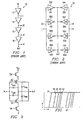
- Figure 1 shows a typical prior art delay chain 10, which may, for example, be part of a ring oscillator.
- the delay chain 10 is made of four delay elements 12, 14, 16, 18 connected in series, as shown.
- An input signal IN is applied to the input of the first delay element 12, and it is passed down the chain 10.
- Each element in the chain 10 gives the input signal a delay of T.
- the signal at the output of delay element 12 has a delay of T with respect to signal IN
- the signal at the output of delay element 14 has a delay of 2T with respect to signal IN
- the signal at the output of delay element 16 has a delay of 3T with respect to signal IN
- the signal at the output of delay element 18 has a delay of 4T with respect to signal IN.
- FIG. 2 shows a typical prior art digital delay interpolator 20.
- the interpolator 20 is made of two groups of delay elements, in this case each being an inverter.
- the first group on the left of the figure, is comprised of four delay elements i1L, i2L, i3L and i4L, of equal strength, each having its input connected to receive a signal L on line 22, while the second group is comprised of four delay elements i1R, i2R, i3R and i4R, of equal strength, each having its input connected to receive a signal R on line 24.
- Each delay element receives a respective differential pair of enable signals Delay elements i1L and i1R receive enable signals EN1 and EN1 , delay elements i2L and i2R receive enable signals EN2 and EN 2 , delay elements i3L and i3R receive enable signals EN3 and EN 3 , while delay elements i4L and i4R receive enable signals EN4 and EN4 .
- the signals L and R may be, for example, the outputs of two adjacent delay elements of the delay chain 10 of Figure 1, such as delay element 12 and delay element 14 for example. In this discussion it is assumed that signal R is delayed more than signal L.
- Delay interpolator 20 functions to cause the timing of its output signal OUT to be controlled incrementally more or less by the timing of signal L or signal R, depending on which of its delay elements are selected for enablement, i.e., their associated enable signal is ON.
- the delay through interpolator 20 may be subdivided into, for example four T/4 delays and thereby provide a finer gradation of delay when used with, for example, the delay chain 10 of Figure 1.
- the delay elements in the interpolator 20 are tristatable inverters and at any given time four out of the eight inverters are ON, i.e., enabled. Minimum delay is achieved when all four inverters receiving the L signal (i1L, i2L, i3L and i4L) are ON.
- the next greater delay is achieved when three inverters receiving L and one inverter receiving R are ON.
- the next greater delay is achieved when two inverters receiving L and two inverters receiving R are ON.
- the next greater delay is achieved when one inverter receiving L and three inverters receiving R are ON.
- Maximum delay is achieved when all four inverters receiving the R signal (i1R, i2R, i3R and i4R) are ON.
- interpolation is to be between a delay of 2T and 3T by selecting the signal from Figure 1 delayed by 2T, i.e., the output of delay element 14, to be signal L and by selecting the signal from Figure 1 delayed by 3T, i.e., the output of delay element 16, to be signal R.
- the inherent delay due to any four of the tristatable inverters driving the output is t.
- delay elements i1R, i2L, i3L and i4L are ON the delay through interpolator 20 is equal to 2T + T/4 + t.
- delay elements i1R, i2R, i3L and i4L are ON the delay through interpolator 20 is equal to 2T + 2T/4 + t.
- delay elements i1R, i2R, i3R and i4R are ON the delay through interpolator 20 is equal to 2T + 4T/4 + t, or, 3T + t.
- the delays expressed above are theoretical delays. In reality, these delays are significantly shorter than expressed above, and these delays vary depending upon the delay selected. This is because of parasitic capacitances in the tristatable inverters, giving rise to capacitance at the interpolated output OUT, and because the capacitive load at output OUT is not the same in all cases.
- any given tristatable inverter in interpolator 20 depends on the voltage at its input, even when it is in the OFF state.
- Figure 3 is a circuit diagram of one of these inverters, each of which has the same construction.
- the capacitance at the output of the inverter is the sum of the gate to drain capacitances of the PMOS transistor 30 and NMOS transistor 32, i.e., C gdp and C gdn , respectively, and of the back gate to drain capacitances of PMOS transistor 30 and NMOS transistor 32, i.e., C bdp and C bdn , respectively.
- transition 34 in Figure 4. A transition delayed by tristate inverters i1L, i2L, i3L and i4L, has this delay. During this transition, signal R is HIGH, and therefore the capacitive load due to tristate inverters i1R, i2R, i3R and i4R, is maximum. The corresponding delay through interpolator 20 is, likewise, maximum.
- transition 42 A transition delayed by tristate inverters i1R, i2R, i3R and i4R, has this delay.
- signal L is completing a transition, and hence the effective capacitive load offered by tristate inverters i1L, i2L, i3L and i4L, is much less than the load in the capacitive load in the previous case.
- the corresponding delay through interpolator 20 is, likewise, minimum.
- the same considerations apply, with decreasing load capacitance, and correspondingly decreasing delay, respectively. This creates a "dead zone" in the delay interpolation by compressing the delays as the transitions are decreasingly delayed.
- the present invention provides an improved digital delay interpolator having uniformly spaced delays.
- a digital delay interpolator adapted to receive a first clock signal and a second clock signal, the second clock signal having a transition at a time that is delayed with respect to the time of a transition of the first clock signal, and to provide an output clock signal having a transition at a time intermediate the time of the transition of the first clock signal and the time of the transition of the second clock signal.
- the interpolator includes a first plurality of selectively enabled delay circuits and a second plurality of selectively enabled delay circuits, the first plurality of delay circuits having an input port being adapted to receive the first clock signal, and the second plurality of delay circuits having an input port being adapted to receive the second clock signal.
- the first plurality of delay circuits and the second plurality of delay circuits have outputs connected together to form the output of the digital delay interpolator.
- Each of the delay circuits includes a first delay buffer element adapted to receive one of the first and second clock signals, and being enabled by an enable signal, a second delay buffer element connected to the output of the first delay buffer, and being enabled by the enable signal, and circuit means for providing a predetermined voltage at the common connection point of the first delay buffer and the second delay buffer when the first and second delay buffers are not enabled.
- a tristatable element circuit being powered by a power supply connected to a ground connection and having a supply voltage.
- a first tristatable circuit element having an input port, an output port and a tristate control port
- a second tristatable circuit element having an input port connected to the output port of the first tristatable circuit element, an output port and a tristate control port.
- a switch coupled between the common connection node of the output of the first tristatable circuit element and the input of the second tristatable circuit element and a voltage source having a magnitude intermediate the supply voltage and ground, and being adapted to be switched to an ON state when the enable signal is OFF.
- a digital delay interpolator of a preferred embodiment of the present invention is shown in Figures 5 and 6.
- another tristate inverter is used to drive each of the previously described tristate inverters in a delay circuit.
- Figure 5 shows one "pair" 50 of such delay circuits, corresponding, to inverters i1L and i1R of Figure 2.
- other pairs of delay elements like those in Figure 5 are also part of this embodiment, interconnected in similar fashion as the tristate inverter pairs of Figure 2, as shown in Figure 6, wherein the three other pairs of delay circuits 60, 70 and 80 are shown, all constituting the digital delay interpolator 100 of this embodiment.
- each of the other such pairs of delay circuits 60, 70 and 80. are of the same construction as that of delay circuit pair 50.
- the main tristate inverter i1L' (corresponding to tristate inverter i1L of Figure 2), the output of which contributes to the output of the interpolator of which it is a part, is now driven by another tristate inverter 52, the input of which receives signal L.
- tristate inverter i1R' the output of which contributes to the output OUT of the interpolator of which it is a part, is now driven by another tristate inverter 54, the input of which receives signal R.
- Both of the "left" inverters 52 and i1L' receive differential enable signals EN1 and EN 1 at their inverting tristate control input, and non-inverting tristate control input, respectively.
- both of the "right" inverters 54 and i1R' receive differential enable signals EN 1 and EN1 at their inverting tristate control input, and non-inverting tristate control input, respectively.
- the signal EN1 is also connected to the gate of an NMOS transistor 56, the source of which is connected to the output of inverter 52, which is also connected to the input of inverter i1L'.
- the drain of transistor 56 is connected to a reference voltage V MID which is near the middle of the level of the supply voltage.
- the signal EN1 is also connected to the gate of an NMOS transistor 58, the source of which is connected to the output of inverter 54, which is also connected to the input of inverter i1R'.
- the drain of transistor 58 is connected to reference voltage V MID .
- the NMOS transistors 56 and 58 function as switches, ensuring that the effective capacitance at the output of the associated inverter i1L' and i1R', respectively, that is disabled is always the same, and is independent of whether the inverter belongs to side L or side R. This maintains a constant and optimized capacitive load, due to the inverters that are in an OFF state, at the output OUT of the interpolator, independent of delay combinations.
- an NMOS switch is used in this embodiment in order to reduce the capacitance offered by the switch to the tristate inverter (e.g., 52) which drives the final tristate inverter (e.g., i1L'). Since an NMOS switch, and not a complete CMOS switch, is used, the V MID reference voltage has been kept lower than mid-supply, to reduce the resistance offered by the NMOS switch, and thereby increase the switching speed.
- the result of this new inventive configuration is the distribution of the subdivision delays of the coarse range T delays uniformly, as shown in Figure 7, which is a diagram like Figure 4, but showing the same signals appearing at the output of an interpolator constructed as in Figure 5. Note that the transitions between the fifth and sixth delayed output signals overlap at 90, as should be the case, and no dead zone is present.
- the fifth transition is the result of inverters i1R, i2R, i3R and i4R, switching, with coarse range signals having delay 2T and 3T (i.e., the outputs of inverters 14 and 16 of Figure 1, respectively) being the signals L and R, respectively.
- the sixth transition is the result of inverters i1L, i2L, i3L and i4L, switching, with coarse range signals having delay 3T and 4T (i.e., the outputs of inverters 16 and 18 of Figure 1, respectively) being the signals L and R, respectively.
- coarse range signals having delay 3T and 4T (i.e., the outputs of inverters 16 and 18 of Figure 1, respectively) being the signals L and R, respectively.
- the V MID voltage may be generated using the MOS-diode chain shown in Figure 8, comprising three PMOS transistors 92, 94 and 96, configured as diodes by having their gates and drains connected together, and connected in series between the supply voltage VCC and ground, as shown.
- the voltage V MID is taken from the common connection point of the drain of transistor 94 and the source of transistor 96, the gate and drain of transistor 96 being connected to ground.
- the preferred embodiment may be used in clock synthesis and other applications in which a high performance digital interpolator is desired.
Landscapes
- Physics & Mathematics (AREA)
- Engineering & Computer Science (AREA)
- Computer Hardware Design (AREA)
- Computing Systems (AREA)
- General Engineering & Computer Science (AREA)
- Mathematical Physics (AREA)
- Nonlinear Science (AREA)
- Pulse Circuits (AREA)
- Logic Circuits (AREA)
- Cable Transmission Systems, Equalization Of Radio And Reduction Of Echo (AREA)
- Dc Digital Transmission (AREA)
Abstract
Description
Claims (6)
- A digital delay interpolator for receiving a first clock signal and a second clock signal, said second clock signal having a transition at a time that is delayed with respect to the time of a transition of said first clock signal, and for providing an output clock signal having a transition at a time intermediate the time of said transition of said first clock signal and the time of said transition of said second clock signal, which interpolator comprising:a first plurality of selectively enabled delay circuits and a second plurality of selectively enabled delay circuits, said first plurality of delay circuits having an input port for receiving said first clock signal, and said second plurality of delay circuits having an input port for receiving said second clock signal, said first plurality of delay circuits and said second plurality of delay circuits having outputs connected together to form the output of said digital delay interpolator, each of said delay circuits comprisinga first delay buffer element for receiving one of said first and second clock signals, and being enabled by an enable signal,a second delay buffer element connected to the output of said first delay buffer, and being enabled by said enable signal, andcircuit means for providing a predetermined voltage at the common connection point of said first delay buffer and said second delay buffer when said first and second delay buffers are not enabled.
- A digital delay interpolator for receiving a first clock signal and a second clock signal, said second clock signal having a transition at a time that is delayed with respect to the time of a transition of said first clock signal, and for providing an output clock signal having a transition at a time intermediate the time of said transition of said first clock signal and the time of said transition of said second clock signal, which interpolator comprising:
a first plurality of selectively enabled delay circuits and a second plurality of selectively enabled delay circuits, said first plurality of delay circuits having an input port for receiving said first clock signal, and said second plurality of delay circuits having an input port for receiving said second clock signal, said first plurality of delay circuits and said second plurality of delay circuits having outputs connected together to form the output of said digital delay interpolator, each of said delay circuits being powered by a power supply having a pair of terminals and comprisinga first selectively enabled delay element having an input port being for receiving said first clock signal, an output port, and an enable port for receiving an enable signal to enable said first delay element when ON,a second selectively enabled delay element having an input port connected to said output port of said first delay element, an output port connected to said output of said interpolator, and an enable port for receiving said enable signal to enable said second delay element when ON,a switch coupled between the common connection node of the output of said first delay element and the input of said second delay element and a voltage source having a magnitude intermediate the voltage level between said pair of terminals, and being adapted to be switched to an ON state when said enable signal is OFF. - A digital delay interpolator according to Claim 1 or Claim 2, wherein each of said selectively enabled delay elements is a tristate inverter.
- A digital delay interpolator according to Claim 2, wherein said switch is a MOS transistor, having a gate for receiving a signal inverse to said enable signal, and being connected between the common connection node of the output of said first delay element and the input of said second delay element and said intermediate magnitude voltage source by way of a drain and a source.
- A tristatable element circuit powered by a power supply connected to a ground connection and having a supply voltage, which circuit comprising:a first tristatable circuit element having an input port, an output port and a tristate control port;a second tristatable circuit element having an input port connected to the output port of said first tristatable circuit element, an output port and a tristate control port; anda switch coupled between the common connection node of the output of said first tristatable circuit element and the input of said second tristatable circuit element and a voltage source having a magnitude intermediate said supply voltage and ground, and being adapted to be switched to an ON state when said enable signal is OFF.
- A tristatable element circuit according to Claim 5, wherein said tristatable circuit elements are tristatable inverters.
Applications Claiming Priority (4)
| Application Number | Priority Date | Filing Date | Title |
|---|---|---|---|
| US18578400P | 2000-02-29 | 2000-02-29 | |
| US185784P | 2000-02-29 | ||
| US755806 | 2001-01-05 | ||
| US09/755,806 US6377102B2 (en) | 2000-02-29 | 2001-01-05 | Load equalization in digital delay interpolators |
Publications (3)
| Publication Number | Publication Date |
|---|---|
| EP1130776A2 true EP1130776A2 (en) | 2001-09-05 |
| EP1130776A3 EP1130776A3 (en) | 2006-02-15 |
| EP1130776B1 EP1130776B1 (en) | 2007-12-26 |
Family
ID=26881469
Family Applications (1)
| Application Number | Title | Priority Date | Filing Date |
|---|---|---|---|
| EP01200733A Expired - Lifetime EP1130776B1 (en) | 2000-02-29 | 2001-02-28 | Load equalization in digital delay interpolators |
Country Status (5)
| Country | Link |
|---|---|
| US (1) | US6377102B2 (en) |
| EP (1) | EP1130776B1 (en) |
| JP (1) | JP2001285042A (en) |
| AT (1) | ATE382206T1 (en) |
| DE (1) | DE60132038T2 (en) |
Cited By (2)
| Publication number | Priority date | Publication date | Assignee | Title |
|---|---|---|---|---|
| WO2003085831A3 (en) * | 2002-03-29 | 2003-11-20 | Intel Corp | A method and apparatus for precise signal interpolation |
| GB2405273A (en) * | 2003-08-04 | 2005-02-23 | Samsung Electronics Co Ltd | A delayed clock signal generator using interpolation between delayed clock phases and compensating for interpolator and selector delay |
Families Citing this family (7)
| Publication number | Priority date | Publication date | Assignee | Title |
|---|---|---|---|---|
| US6984934B2 (en) * | 2001-07-10 | 2006-01-10 | The Trustees Of Princeton University | Micro-lens arrays for display intensity enhancement |
| US20040246030A1 (en) * | 2003-06-06 | 2004-12-09 | Yang Steven Jyh-Ren | Speeded up multistage comparator with power reduction and reliable output |
| US7453302B2 (en) * | 2003-12-23 | 2008-11-18 | Infineon Technologies Ag | Temperature compensated delay signals |
| US7622961B2 (en) * | 2005-09-23 | 2009-11-24 | Intel Corporation | Method and apparatus for late timing transition detection |
| DE102006053322B3 (en) * | 2006-11-13 | 2008-03-27 | Texas Instruments Deutschland Gmbh | Buffer chain driver for driving clock pulses over mismatched transmission line, has two signal paths, which are formed by buffer-cells connected in series, and resistor elements are connected in output of inverter level of two signal paths |
| US20130200937A1 (en) * | 2012-02-07 | 2013-08-08 | International Business Machines Corporation | Delay line with cell by cell power down capability |
| CN113098453B (en) * | 2021-04-06 | 2022-02-18 | 无锡中微亿芯有限公司 | A phase interpolation circuit |
Family Cites Families (18)
| Publication number | Priority date | Publication date | Assignee | Title |
|---|---|---|---|---|
| EP0390226A1 (en) * | 1984-07-31 | 1990-10-03 | Yamaha Corporation | Jitter absorption circuit |
| US4899071A (en) * | 1988-08-02 | 1990-02-06 | Standard Microsystems Corporation | Active delay line circuit |
| JPH0282713A (en) * | 1988-09-19 | 1990-03-23 | Fujitsu Ltd | Switching auxiliary circuit |
| JP3426608B2 (en) * | 1990-04-04 | 2003-07-14 | ユニシス コーポレイシヨン | Clock deskew circuit |
| KR940008718B1 (en) * | 1991-10-25 | 1994-09-26 | 삼성전자 주식회사 | Data output buffer having reduced direct current |
| US5227679A (en) * | 1992-01-02 | 1993-07-13 | Advanced Micro Devices, Inc. | Cmos digital-controlled delay gate |
| FR2688783A1 (en) * | 1992-03-23 | 1993-09-24 | Rhone Poulenc Chimie | NOVEL BORONES OF ONIUM OR ORGANOMETALLIC COMPLEX CATIONIC PRIMERS FOR POLYMERIZATION. |
| EP0585505B1 (en) * | 1992-06-26 | 2001-10-31 | STMicroelectronics S.r.l. | Low noise buffer |
| JP2905669B2 (en) * | 1993-07-20 | 1999-06-14 | シャープ株式会社 | Delay circuit |
| US5489864A (en) * | 1995-02-24 | 1996-02-06 | Intel Corporation | Delay interpolation circuitry |
| US5644262A (en) * | 1995-02-24 | 1997-07-01 | Intel Corporation | Digitally controlled capacitive load |
| US5748125A (en) * | 1996-01-23 | 1998-05-05 | International Business Machines Corporation | Digital delay interpolator circuit |
| US5694377A (en) * | 1996-04-16 | 1997-12-02 | Ltx Corporation | Differential time interpolator |
| US5748542A (en) * | 1996-12-13 | 1998-05-05 | Micron Technology, Inc. | Circuit and method for providing a substantially constant time delay over a range of supply voltages |
| US6023181A (en) * | 1997-04-25 | 2000-02-08 | Texas Instruments Incorporated | High speed unitransition input buffer |
| US5963074A (en) * | 1997-06-18 | 1999-10-05 | Credence Systems Corporation | Programmable delay circuit having calibratable delays |
| US5982213A (en) * | 1997-11-14 | 1999-11-09 | Texas Instruments Incorporated | Digital phase lock loop |
| US6163195A (en) * | 1998-05-26 | 2000-12-19 | Altera Corporation | Temperature compensated delay chain |
-
2001
- 2001-01-05 US US09/755,806 patent/US6377102B2/en not_active Expired - Lifetime
- 2001-02-28 EP EP01200733A patent/EP1130776B1/en not_active Expired - Lifetime
- 2001-02-28 JP JP2001054983A patent/JP2001285042A/en not_active Abandoned
- 2001-02-28 DE DE60132038T patent/DE60132038T2/en not_active Expired - Lifetime
- 2001-02-28 AT AT01200733T patent/ATE382206T1/en not_active IP Right Cessation
Cited By (4)
| Publication number | Priority date | Publication date | Assignee | Title |
|---|---|---|---|---|
| WO2003085831A3 (en) * | 2002-03-29 | 2003-11-20 | Intel Corp | A method and apparatus for precise signal interpolation |
| GB2405273A (en) * | 2003-08-04 | 2005-02-23 | Samsung Electronics Co Ltd | A delayed clock signal generator using interpolation between delayed clock phases and compensating for interpolator and selector delay |
| GB2405273B (en) * | 2003-08-04 | 2006-06-28 | Samsung Electronics Co Ltd | Delayed clock signal generator |
| US7106117B2 (en) | 2003-08-04 | 2006-09-12 | Samsung Electronics Co., Ltd. | Delayed clock signal generator |
Also Published As
| Publication number | Publication date |
|---|---|
| DE60132038T2 (en) | 2008-12-11 |
| US20010030566A1 (en) | 2001-10-18 |
| DE60132038D1 (en) | 2008-02-07 |
| EP1130776B1 (en) | 2007-12-26 |
| US6377102B2 (en) | 2002-04-23 |
| JP2001285042A (en) | 2001-10-12 |
| EP1130776A3 (en) | 2006-02-15 |
| ATE382206T1 (en) | 2008-01-15 |
Similar Documents
| Publication | Publication Date | Title |
|---|---|---|
| US7245153B2 (en) | Level shift circuit having timing adjustment circuit for maintaining duty ratio | |
| JP3955150B2 (en) | Phase interpolator, timing signal generation circuit, semiconductor integrated circuit device and semiconductor integrated circuit system to which the timing signal generation circuit is applied | |
| JP4922248B2 (en) | System and method for level shifting using an AC connection | |
| EP1146643A2 (en) | Phase shifter for use in a quadrature clock generator | |
| KR100933609B1 (en) | Transmitter | |
| JP3575430B2 (en) | Two-stage variable length delay circuit | |
| TWI589123B (en) | Phase mixing circuit, and semiconductor apparatus and semiconductor system including the same | |
| US9054578B2 (en) | Hybrid driver including a turbo mode | |
| KR102624454B1 (en) | Data serializer circuit | |
| US6909317B2 (en) | Clock control circuit and method | |
| KR100715845B1 (en) | Phase Mixer and Multiphase Generator Using the Same | |
| US7667502B2 (en) | Low voltage differential signalling driver with pre-emphasis | |
| US6377102B2 (en) | Load equalization in digital delay interpolators | |
| KR20000008998A (en) | Output buffer and its buffering method | |
| US7973681B2 (en) | High speed, low power non-return-to-zero/return-to-zero output driver | |
| EP0865160B1 (en) | Interpolating circuit | |
| JPH09284125A (en) | Variable delay circuit | |
| JP3850470B2 (en) | Slew rate control drive circuit | |
| WO2002056474A2 (en) | Clock interpolation through capacitive weighting | |
| JP3190199B2 (en) | In-phase signal output circuit, anti-phase signal output circuit, two-phase signal output circuit, and signal output circuit | |
| US6456126B1 (en) | Frequency doubler with polarity control | |
| WO2017136052A2 (en) | Compact phase interpolator | |
| JP2845192B2 (en) | Differential switching circuit | |
| KR100625911B1 (en) | Clock Control Circuit | |
| JPH11346144A (en) | Delay circuit |
Legal Events
| Date | Code | Title | Description |
|---|---|---|---|
| PUAI | Public reference made under article 153(3) epc to a published international application that has entered the european phase |
Free format text: ORIGINAL CODE: 0009012 |
|
| 17P | Request for examination filed |
Effective date: 20010228 |
|
| AK | Designated contracting states |
Kind code of ref document: A2 Designated state(s): AT BE CH CY DE DK ES FI FR GB GR IE IT LI LU MC NL PT SE TR |
|
| AX | Request for extension of the european patent |
Free format text: AL;LT;LV;MK;RO;SI |
|
| PUAL | Search report despatched |
Free format text: ORIGINAL CODE: 0009013 |
|
| AK | Designated contracting states |
Kind code of ref document: A3 Designated state(s): AT BE CH CY DE DK ES FI FR GB GR IE IT LI LU MC NL PT SE TR |
|
| AX | Request for extension of the european patent |
Extension state: AL LT LV MK RO SI |
|
| RIC1 | Information provided on ipc code assigned before grant |
Ipc: H03K 19/003 20060101ALI20051223BHEP Ipc: H03K 5/13 20060101AFI20010607BHEP Ipc: H03L 7/081 20060101ALI20051223BHEP |
|
| AKX | Designation fees paid |
Designated state(s): AT BE CH CY DE DK ES FI FR GB GR IE IT LI LU MC NL PT SE TR |
|
| 17Q | First examination report despatched |
Effective date: 20061123 |
|
| GRAP | Despatch of communication of intention to grant a patent |
Free format text: ORIGINAL CODE: EPIDOSNIGR1 |
|
| GRAS | Grant fee paid |
Free format text: ORIGINAL CODE: EPIDOSNIGR3 |
|
| GRAA | (expected) grant |
Free format text: ORIGINAL CODE: 0009210 |
|
| AK | Designated contracting states |
Kind code of ref document: B1 Designated state(s): AT BE CH CY DE DK ES FI FR GB GR IE IT LI LU MC NL PT SE TR |
|
| REG | Reference to a national code |
Ref country code: GB Ref legal event code: FG4D |
|
| REG | Reference to a national code |
Ref country code: IE Ref legal event code: FG4D |
|
| REG | Reference to a national code |
Ref country code: CH Ref legal event code: EP |
|
| REF | Corresponds to: |
Ref document number: 60132038 Country of ref document: DE Date of ref document: 20080207 Kind code of ref document: P |
|
| PG25 | Lapsed in a contracting state [announced via postgrant information from national office to epo] |
Ref country code: LI Free format text: LAPSE BECAUSE OF FAILURE TO SUBMIT A TRANSLATION OF THE DESCRIPTION OR TO PAY THE FEE WITHIN THE PRESCRIBED TIME-LIMIT Effective date: 20071226 Ref country code: SE Free format text: LAPSE BECAUSE OF FAILURE TO SUBMIT A TRANSLATION OF THE DESCRIPTION OR TO PAY THE FEE WITHIN THE PRESCRIBED TIME-LIMIT Effective date: 20080326 Ref country code: CH Free format text: LAPSE BECAUSE OF FAILURE TO SUBMIT A TRANSLATION OF THE DESCRIPTION OR TO PAY THE FEE WITHIN THE PRESCRIBED TIME-LIMIT Effective date: 20071226 |
|
| PG25 | Lapsed in a contracting state [announced via postgrant information from national office to epo] |
Ref country code: NL Free format text: LAPSE BECAUSE OF FAILURE TO SUBMIT A TRANSLATION OF THE DESCRIPTION OR TO PAY THE FEE WITHIN THE PRESCRIBED TIME-LIMIT Effective date: 20071226 Ref country code: FI Free format text: LAPSE BECAUSE OF FAILURE TO SUBMIT A TRANSLATION OF THE DESCRIPTION OR TO PAY THE FEE WITHIN THE PRESCRIBED TIME-LIMIT Effective date: 20071226 |
|
| NLV1 | Nl: lapsed or annulled due to failure to fulfill the requirements of art. 29p and 29m of the patents act | ||
| REG | Reference to a national code |
Ref country code: CH Ref legal event code: PL |
|
| PG25 | Lapsed in a contracting state [announced via postgrant information from national office to epo] |
Ref country code: AT Free format text: LAPSE BECAUSE OF FAILURE TO SUBMIT A TRANSLATION OF THE DESCRIPTION OR TO PAY THE FEE WITHIN THE PRESCRIBED TIME-LIMIT Effective date: 20071226 |
|
| ET | Fr: translation filed | ||
| PG25 | Lapsed in a contracting state [announced via postgrant information from national office to epo] |
Ref country code: ES Free format text: LAPSE BECAUSE OF FAILURE TO SUBMIT A TRANSLATION OF THE DESCRIPTION OR TO PAY THE FEE WITHIN THE PRESCRIBED TIME-LIMIT Effective date: 20080406 |
|
| PG25 | Lapsed in a contracting state [announced via postgrant information from national office to epo] |
Ref country code: BE Free format text: LAPSE BECAUSE OF FAILURE TO SUBMIT A TRANSLATION OF THE DESCRIPTION OR TO PAY THE FEE WITHIN THE PRESCRIBED TIME-LIMIT Effective date: 20071226 |
|
| PG25 | Lapsed in a contracting state [announced via postgrant information from national office to epo] |
Ref country code: PT Free format text: LAPSE BECAUSE OF FAILURE TO SUBMIT A TRANSLATION OF THE DESCRIPTION OR TO PAY THE FEE WITHIN THE PRESCRIBED TIME-LIMIT Effective date: 20080526 |
|
| PG25 | Lapsed in a contracting state [announced via postgrant information from national office to epo] |
Ref country code: MC Free format text: LAPSE BECAUSE OF NON-PAYMENT OF DUE FEES Effective date: 20080228 Ref country code: DK Free format text: LAPSE BECAUSE OF FAILURE TO SUBMIT A TRANSLATION OF THE DESCRIPTION OR TO PAY THE FEE WITHIN THE PRESCRIBED TIME-LIMIT Effective date: 20071226 |
|
| PLBE | No opposition filed within time limit |
Free format text: ORIGINAL CODE: 0009261 |
|
| STAA | Information on the status of an ep patent application or granted ep patent |
Free format text: STATUS: NO OPPOSITION FILED WITHIN TIME LIMIT |
|
| 26N | No opposition filed |
Effective date: 20080929 |
|
| PG25 | Lapsed in a contracting state [announced via postgrant information from national office to epo] |
Ref country code: IE Free format text: LAPSE BECAUSE OF NON-PAYMENT OF DUE FEES Effective date: 20080228 Ref country code: GR Free format text: LAPSE BECAUSE OF FAILURE TO SUBMIT A TRANSLATION OF THE DESCRIPTION OR TO PAY THE FEE WITHIN THE PRESCRIBED TIME-LIMIT Effective date: 20080327 |
|
| PG25 | Lapsed in a contracting state [announced via postgrant information from national office to epo] |
Ref country code: CY Free format text: LAPSE BECAUSE OF FAILURE TO SUBMIT A TRANSLATION OF THE DESCRIPTION OR TO PAY THE FEE WITHIN THE PRESCRIBED TIME-LIMIT Effective date: 20071226 |
|
| PG25 | Lapsed in a contracting state [announced via postgrant information from national office to epo] |
Ref country code: LU Free format text: LAPSE BECAUSE OF NON-PAYMENT OF DUE FEES Effective date: 20080228 |
|
| PG25 | Lapsed in a contracting state [announced via postgrant information from national office to epo] |
Ref country code: TR Free format text: LAPSE BECAUSE OF FAILURE TO SUBMIT A TRANSLATION OF THE DESCRIPTION OR TO PAY THE FEE WITHIN THE PRESCRIBED TIME-LIMIT Effective date: 20071226 |
|
| PG25 | Lapsed in a contracting state [announced via postgrant information from national office to epo] |
Ref country code: IT Free format text: LAPSE BECAUSE OF NON-PAYMENT OF DUE FEES Effective date: 20080229 |
|
| REG | Reference to a national code |
Ref country code: FR Ref legal event code: PLFP Year of fee payment: 16 |
|
| PGFP | Annual fee paid to national office [announced via postgrant information from national office to epo] |
Ref country code: DE Payment date: 20160302 Year of fee payment: 16 |
|
| PGFP | Annual fee paid to national office [announced via postgrant information from national office to epo] |
Ref country code: FR Payment date: 20160125 Year of fee payment: 16 Ref country code: GB Payment date: 20160127 Year of fee payment: 16 |
|
| REG | Reference to a national code |
Ref country code: DE Ref legal event code: R119 Ref document number: 60132038 Country of ref document: DE |
|
| GBPC | Gb: european patent ceased through non-payment of renewal fee |
Effective date: 20170228 |
|
| REG | Reference to a national code |
Ref country code: FR Ref legal event code: ST Effective date: 20171031 |
|
| PG25 | Lapsed in a contracting state [announced via postgrant information from national office to epo] |
Ref country code: FR Free format text: LAPSE BECAUSE OF NON-PAYMENT OF DUE FEES Effective date: 20170228 Ref country code: DE Free format text: LAPSE BECAUSE OF NON-PAYMENT OF DUE FEES Effective date: 20170901 |
|
| PG25 | Lapsed in a contracting state [announced via postgrant information from national office to epo] |
Ref country code: GB Free format text: LAPSE BECAUSE OF NON-PAYMENT OF DUE FEES Effective date: 20170228 |