EP1130723A2 - Semiconductor laser device and method for manufacturing the same - Google Patents
Semiconductor laser device and method for manufacturing the same Download PDFInfo
- Publication number
- EP1130723A2 EP1130723A2 EP01301871A EP01301871A EP1130723A2 EP 1130723 A2 EP1130723 A2 EP 1130723A2 EP 01301871 A EP01301871 A EP 01301871A EP 01301871 A EP01301871 A EP 01301871A EP 1130723 A2 EP1130723 A2 EP 1130723A2
- Authority
- EP
- European Patent Office
- Prior art keywords
- layer
- semiconductor laser
- diffraction grating
- laser device
- current blocking
- Prior art date
- Legal status (The legal status is an assumption and is not a legal conclusion. Google has not performed a legal analysis and makes no representation as to the accuracy of the status listed.)
- Withdrawn
Links
Images







Classifications
-
- H—ELECTRICITY
- H01—ELECTRIC ELEMENTS
- H01S—DEVICES USING THE PROCESS OF LIGHT AMPLIFICATION BY STIMULATED EMISSION OF RADIATION [LASER] TO AMPLIFY OR GENERATE LIGHT; DEVICES USING STIMULATED EMISSION OF ELECTROMAGNETIC RADIATION IN WAVE RANGES OTHER THAN OPTICAL
- H01S5/00—Semiconductor lasers
- H01S5/10—Construction or shape of the optical resonator, e.g. extended or external cavity, coupled cavities, bent-guide, varying width, thickness or composition of the active region
- H01S5/12—Construction or shape of the optical resonator, e.g. extended or external cavity, coupled cavities, bent-guide, varying width, thickness or composition of the active region the resonator having a periodic structure, e.g. in distributed feedback [DFB] lasers
-
- H—ELECTRICITY
- H01—ELECTRIC ELEMENTS
- H01S—DEVICES USING THE PROCESS OF LIGHT AMPLIFICATION BY STIMULATED EMISSION OF RADIATION [LASER] TO AMPLIFY OR GENERATE LIGHT; DEVICES USING STIMULATED EMISSION OF ELECTROMAGNETIC RADIATION IN WAVE RANGES OTHER THAN OPTICAL
- H01S5/00—Semiconductor lasers
- H01S5/20—Structure or shape of the semiconductor body to guide the optical wave ; Confining structures perpendicular to the optical axis, e.g. index or gain guiding, stripe geometry, broad area lasers, gain tailoring, transverse or lateral reflectors, special cladding structures, MQW barrier reflection layers
- H01S5/22—Structure or shape of the semiconductor body to guide the optical wave ; Confining structures perpendicular to the optical axis, e.g. index or gain guiding, stripe geometry, broad area lasers, gain tailoring, transverse or lateral reflectors, special cladding structures, MQW barrier reflection layers having a ridge or stripe structure
- H01S5/223—Buried stripe structure
- H01S5/2231—Buried stripe structure with inner confining structure only between the active layer and the upper electrode
-
- H—ELECTRICITY
- H01—ELECTRIC ELEMENTS
- H01S—DEVICES USING THE PROCESS OF LIGHT AMPLIFICATION BY STIMULATED EMISSION OF RADIATION [LASER] TO AMPLIFY OR GENERATE LIGHT; DEVICES USING STIMULATED EMISSION OF ELECTROMAGNETIC RADIATION IN WAVE RANGES OTHER THAN OPTICAL
- H01S5/00—Semiconductor lasers
- H01S5/20—Structure or shape of the semiconductor body to guide the optical wave ; Confining structures perpendicular to the optical axis, e.g. index or gain guiding, stripe geometry, broad area lasers, gain tailoring, transverse or lateral reflectors, special cladding structures, MQW barrier reflection layers
- H01S5/2054—Methods of obtaining the confinement
- H01S5/2081—Methods of obtaining the confinement using special etching techniques
- H01S5/209—Methods of obtaining the confinement using special etching techniques special etch stop layers
-
- H—ELECTRICITY
- H01—ELECTRIC ELEMENTS
- H01S—DEVICES USING THE PROCESS OF LIGHT AMPLIFICATION BY STIMULATED EMISSION OF RADIATION [LASER] TO AMPLIFY OR GENERATE LIGHT; DEVICES USING STIMULATED EMISSION OF ELECTROMAGNETIC RADIATION IN WAVE RANGES OTHER THAN OPTICAL
- H01S5/00—Semiconductor lasers
- H01S5/30—Structure or shape of the active region; Materials used for the active region
- H01S5/32—Structure or shape of the active region; Materials used for the active region comprising PN junctions, e.g. hetero- or double- heterostructures
- H01S5/323—Structure or shape of the active region; Materials used for the active region comprising PN junctions, e.g. hetero- or double- heterostructures in AIIIBV compounds, e.g. AlGaAs-laser, InP-based laser
- H01S5/32308—Structure or shape of the active region; Materials used for the active region comprising PN junctions, e.g. hetero- or double- heterostructures in AIIIBV compounds, e.g. AlGaAs-laser, InP-based laser emitting light at a wavelength less than 900 nm
- H01S5/32316—Structure or shape of the active region; Materials used for the active region comprising PN junctions, e.g. hetero- or double- heterostructures in AIIIBV compounds, e.g. AlGaAs-laser, InP-based laser emitting light at a wavelength less than 900 nm comprising only (Al)GaAs
Definitions
- the present invention relates to distributed feedback semiconductor lasers and distributed Bragg reflector semiconductor lasers.
- DBR distributed Bragg reflector
- a structure for transversal mode control and current confinement in which a stripe-shaped recess portion (so-called window) is formed in the current blocking layer, as disclosed for example in JP H06-112580A.
- window a stripe-shaped recess portion
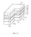
- This DFB semiconductor laser includes an n-type GaAs substrate 101, and formed on top thereof an n-type GaAs buffer layer 102, an n-type Ga 0.5 Al 0.5 As first cladding layer 103, a Ga 0.85 Al 0.15 As active layer 104, a p-type Ga 0.5 Al 0.5 As first optical guiding layer 105, and a p-type Ga 0.8 Al 0.2 As diffraction grating layer 106. Formed on top of that are an n-type Ga 0.4 Al 0.6 As current blocking layer 109 having a stripe-shaped window 109a for current confinement, and a p-type GaAs protective layer 112. Furthermore, a p-type Ga 0.5 Al 0.5 As second cladding layer 110 and a p-type GaAs contact layer 111 are formed on top of the protective layer 112 and the stripe-shaped window 109a.
- a diffraction layer 106 having a diffraction grating 106a is formed below the active layer 104.
- DBR semiconductor lasers having a different structure to ensure single longitudinal mode oscillation.
- the following is an explanation of a method for manufacturing such a semiconductor, with reference to Fig. 12.
- an n-type GaAs buffer layer 143, an n-type Ga 0.5 Al 0.5 As first cladding layer 144, a Ga 0.85 Al 0.15 As active layer 145, a p-type Ga 0.5 Al 0.5 As second cladding layer 146, and a grating layer 147 are formed on top of an n-type GaAs substrate 142 in a first crystal growth process.
- a diffraction grating 147a is formed in the grating layer 147 in a distributed Bragg reflection region 141 by etching the grating layer 147 in this distributed Bragg reflection region 141.
- a p-type Ga 0.5 Al 0.5 As third cladding layer 148 is formed in a second crystal growth process, and a ridge 148a extending in a direction perpendicular to the diffraction grating is formed by etching the p-type Ga 0.5 Al 0.5 As third cladding layer 148.
- a SiO 2 film 150 is formed on the ridge 148a, and using this SiO 2 film 150 as a mask for selective growth, an n-type GaAs current blocking layer 149 is formed on the p-type Ga 0.5 Al 0.5 As third cladding layer 148 in a third crystal growth process.
- the SiO 2 film 150 is eliminated by selective etching, and a p-type GaAs contact layer 151 is formed in a fourth crystal growth process.
- a diffraction grating having a periodic structure is formed in the grating layer 147 in the distributed Bragg reflection region 141, so that single longitudinal mode oscillation is possible.
- the forbidden band width of the n-type GaAs current blocking layer 149 is smaller than the energy of the laser light wavelength, so that the laser light is absorbed by the n-type GaAs current blocking layer 149 in the region outside the ridge 148a, the laser light is confined in the ridge 148a and laser oscillation in a single transverse mode is achieved.
- the grating layer is formed between the cladding layers, so that four crystal growth processes have to be carried out, which makes the manufacturing process complicated and lowers the yield. Furthermore, because of the optical absorption of the current blocking layer, the waveguide loss is high, and there is the problem that the operating current is large. In addition, because of the optical absorption of the current blocking layer, the optical distribution is limited, and there is the problem that it is difficult to achieve a large coupling coefficient.
- a first semiconductor laser device in accordance with the present invention includes a substrate; an active layer formed on the substrate; a semiconductor layer provided with a diffraction grating formed on the active layer; an etch-stop layer formed on the semiconductor layer; a cladding layer provided with a stripe structure, formed on the etch-stop layer; and a current blocking layer formed on the etch-stop layer and arranged at least on a side of said stripe structure.
- the etch-stop layer is formed on the semiconductor layer with the diffraction grating, so that damage to the diffraction grating due to the etching can be prevented.
- the refractive index of the current blocking layer is lower than the refractive index of the cladding layer, because this can reduce waveguide losses of the semiconductor laser by suppressing the absorption of laser light by the current blocking layer, and the distribution of the laser light can extend into the diffraction grating below the current blocking layer, so that the coupling coefficient of the diffraction grating can be increased.
- the etch-stop layer is a Ga 1-S Al S As layer of a first conductivity type
- the current blocking layer is a Ga 1-Z Al Z As layer of a second conductivity type
- the cladding layer is a Ga 1-C Al C As layer of the first conductivity type
- the relation between C, S, and Z is 1 ⁇ Z > C > S ⁇ 0.
- the Al composition ratio S of the etch-stop layer is smaller than the Al composition ratios Z and C of the current blocking layer and the cladding layer, which are etched layers, so that during the etching of those etched layers, etching of the diffraction grating layer can be prevented with the etch-stop layer.
- the Al composition ratio Z of the current blocking layer is larger than the Al composition ratio C of the cladding layer, so that, as mentioned above, the absorption of laser light by the current blocking layer can be prevented, and the laser light distribution in the diffraction grating below the current blocking layer can be expanded.
- a method for manufacturing the first semiconductor laser device in accordance with the present invention includes forming an etch-stop layer of Ga 1-S Al S As; forming an etched layer selected from the cladding layer and the current blocking layer of Ga 1-U Al U As (with 1 ⁇ U > S ⁇ 0); and forming a stripe structure by etching this etched layer with an etchant that selectively etches GaAlAs layers with a higher Al composition ratio.
- an etchant is used that selectively etches GaAlAs layers with a higher Al ratio (in other words, with higher AlAs crystal composition ratio), and the Al composition ratio of the layers is controlled as described above, so that the etching is stopped by the etch-stop layer, and over-etching of the diffraction grating layer below the etch-stop layer can be prevented. If the etched layer is the current blocking layer, then U corresponds to Z, and if the etched layer is the cladding layer, then U corresponds to C.
- the semiconductor laser device further includes a first optical guiding layer of Ga 1-Y1 Al Y1 As (0 ⁇ Y1 ⁇ 1) of the first conductivity type between the active layer and the diffraction grating layer. It is also preferable that the semiconductor laser device further includes a second optical guiding layer of Ga 1-Y2 Al Y2 As (0 ⁇ Y2 ⁇ 1) of the first conductivity type between the semiconductor layer with the diffraction grating and the etch-stop layer. It is preferable that the semiconductor layer with the diffraction grating is a layer of Ga 1-G Al G As (0 ⁇ G ⁇ 1), and the relation between G and Y2 is Y2 > G. It is further preferable that the active layer has a quantum well structure including quantum well layers made of Ga 1-X Al X As (0 ⁇ X ⁇ 1).
- a second semiconductor laser device of the present invention is a DBR semiconductor laser device and includes an active layer formed on a substrate, and a current blocking layer formed on the active layer having. and a stripe-shaped window, wherein a diffraction grating is formed at least near an end face in the current blocking layer.
- a diffraction grating is formed in the current blocking layer. Therefore, the diffraction grating is formed after forming all layers up to the current blocking layer, and manufacturing can be completed in one further crystal growth process. Since the diffraction grating is formed in the current blocking layer, laser light leaks into the current blocking layer and is propagated, so that the coupling coefficient of the grating element can be made larger.
- a method for manufacturing this second DBR semiconductor laser device of the present invention includes forming the current blocking layer on the active layer, partially removing the current blocking layer to form the stripe-shaped window, and forming the diffraction grating at least in a region of the current blocking layer that is near an end face. With this manufacturing method, a DBR semiconductor laser device can be manufactured in which the growth of the layers does not have to be interrupted after forming the diffraction grating.
- an n-type GaAs buffer layer 2 an n-type Ga 0.5 Al 0.5 As first cladding layer 3, a Ga 0.85 Al 0.15 As active layer 4, a p-type Ga 0.5 Al 0.5 As first optical guiding layer 5, a p-type Ga 0.8 Al 0.2 As diffraction grating layer 6, a p-type Ga 0.5 Al 0.5 As second optical guiding layer 7, and a p-type Ga 0.8 Al 0.2 As etch-stop layer 8 are formed in that order on top of an n-type GaAs substrate 1. Formed on top of that layering structure is an n-type Ga 0.4 Al 0.6 As current blocking layer 9 having a stripe-shaped window 9a for current confinement. Furthermore, a p-type Ga 0.5 Al 0.5 As second cladding layer 10 and a p-type GaAs contact layer 11 are formed on the current blocking layer 9 and the stripe-shaped window 9a.
- the current injected from the p-type GaAs contact layer 11 is confined by the n-type Ga 0.4 Al 0.6 As current blocking layer 9 in the stripe-shaped window 9a, and laser oscillation in the 780nm band occurs in the active layer 4 below the stripe-shaped window 9a.
- the forbidden band width of the Ga 0.4 Al 0.6 As current blocking layer 9 is larger than the forbidden band width of the Ga 0.85 Al 0.15 As active layer 4 and the p-type Ga 0.5 Al 0.5 As second cladding layer 10, so that there is almost no absorption of laser light by the current blocking layer 9. Consequently, waveguide losses can be reduced considerably.
- the optical distribution of the laser light is not limited to the space inside the stripe, but extends into the diffraction grating layer below the current blocking layer 9. Consequently, the optical power propagating through the diffraction grating is increased, and it is possible to set a higher coupling coefficient of the diffraction grating, which determines wavelength selectivity. As a result, a superior wavelength selectivity can be accomplished with the diffraction grating 6a, and a single longitudinal mode can be sustained that is not susceptible to changes in temperature or optical output.
- the AlAs crystal composition ratio in the current blocking layer 9 is set higher than the AlAs crystal composition ratio in the second cladding layer 10, to prevent the formation of an antiguide waveguide caused by a decreasing refractive index in the stripe due to the plasma effect during current injection.
- the AlAs crystal composition ratio in the current blocking layer 9 is set to 0.6, which is higher than the AlAs crystal composition ratio in the Ga 0.5 Al 0.5 As second cladding layer 10.
- the AlAs crystal composition ratio in the Ga 0.5 Al 0.5 As first optical guiding layer 5 is set considerably higher than the AlAs crystal composition ratio in the active layer 4, so that the carriers are effectively confined in the active layer 4.
- an AlAs crystal composition ratio of at least 0.45 is preferable, and in this embodiment, it is set to 0.5.
- the AlAs crystal composition ratio of the Ga 0.8 Al 0.2 As etch-stop layer 8 is not higher than 0.3, so that the etching selectivity ratio toward the Ga 0.5 Al 0.5 As second cladding layer 10 is high and regrowth thereon is easy. It is also preferable that the etch-stop layer 8 does not absorb the oscillation wavelength of the laser. In the present embodiment, the AlAs crystal composition ratio of the Ga 0.8 Al 0.2 As etch-stop layer 8 is set to 0.2.
- the diffraction grating 6a formed in the diffraction grating layer 6 is formed periodically in the direction of the optical resonator.
- the period of the diffraction grating is an integer multiple of the wavelength in the medium.
- Certain wavelengths of the laser light propagating through the optical resonator are selected by Bragg reflection with the diffraction grating 6a.
- the refractive index difference between the Ga 0.8 Al 0.2 As diffraction grating layer 6 and the Ga 0.5 Al 0.5 As second optical guiding layer 7, in which the diffraction grating 6a is buried, determines the wavelength selection with the diffraction grating 6a.
- the AlAs crystal composition ratio of the diffraction grating layer 6 is not higher than 0.3, so that a favorable wavelength selectivity is achieved and regrowth on the diffraction grating layer 6 is easy, and it is preferable that the diffraction grating layer 6 does not absorb the oscillation wavelength of the laser.
- the AlAs crystal composition ratio of the diffraction grating layer 6 is set to 0.2.
- the AlAs crystal composition ratio of the second optical guiding layer 7 is at least 0.5, so that the refractive index difference with respect to the diffraction grating layer 6 is sufficient for single longitudinal modes. In the present invention, it is set to 0.5.
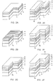
- Figs. 2A to 2F illustrate the manufacturing process for a DFB semiconductor laser in accordance with this embodiment.
- an n n-type GaAs buffer layer 2 (of 0.5 ⁇ m thickness), an n-type Ga 0.5 Al 0.5 As first cladding layer 3 (of 1 ⁇ m thickness), a multi-quantum well active layer 4 of Ga 0.7 Al 0.3 As barrier layers and GaAs well layers, a p-type Ga 0.5 Al 0.5 As first optical guiding layer 5 (of 0.06 ⁇ m thickness), and a p-type Ga 0.8 Al 0.2 As diffraction grating layer 6 (of 0.06 ⁇ m thickness) are formed on an n-type GaAs substrate 1 in a first crystal growth process by MOCVD or MBE. It should be noted that throughout this specification layer thicknesses are only given as examples, and the present invention is in no way limited by these numerical values.
- Unstrained multiple quantum wells are used for the active layer in the present embodiment, but it is also possible to use strained quantum wells or bulk material. Furthermore, the active layer can be p-type or n-type, or even undoped.
- a diffraction grating 6a that is periodic in the direction of the optical resonator is formed in the diffraction grating layer 6 by interference exposure or electron beam exposure and wet etching or dry etching.
- a p-type Ga 0.5 Al 0.5 As second optical guiding layer 7 (of 0.06 ⁇ m thickness), a p-type Ga 0.8 Al 0.2 As etch-stop layer 8 (of 0.01 ⁇ m thickness), and an n-type Ga 0.4 Al 0.6 As current blocking layer 9 (of 0.6 ⁇ m thickness) are formed in a second crystal growth process on the diffraction grating layer 6.
- the current blocking layer 9 is too thin, then the confinement of the light in transversal direction becomes too weak, so that the transversal mode becomes unstable. It is preferable that the thickness of the current blocking layer 9 is at least 0.4 ⁇ m.
- a striped shaped window 9a for current confinement is formed by etching in the Ga 0.4 Al 0.6 As current blocking layer 9.
- an etchant such as hydrofluoric acid, which selectively etches layers with a high AlAs crystal composition ratio, it is possible to stop the etching with the etch-stop layer 8 having the composition Ga 0.8 Al 0.2 As. Therefore, variations in the characteristics due to the etching do not occur, and it is possible to obtain a semiconductor laser suitable for mass production with high yield.
- the diffraction grating layer 6 and the etch-stop layer 8 are formed separately, so that the shape of the diffraction grating 6a is not degraded by the etching of the stripe.
- a regular mesa shape is preferable to an inverted mesa shape, because with the regular mesa shape, crystal growth for filling up the stripe groove is easier, and the yield can be increased.
- a p-type Ga 0.5 Al 0.5 As second cladding layer 10 (of 2 ⁇ m thickness) and a p-type GaAs contact layer 11 (of 2 ⁇ m thickness) are formed on the current blocking layer 9 including the stripe shaped window, as shown in Fig. 2E.
- n-electrode 21 and a p-electrode 22 are formed on the n-type GaAs substrate 1 and the p-type GaAs contact layer 11 respectively, as shown in Fig. 2F.
- a coating of low reflectivity of 5% can be applied to the front facet of the laser where the laser light is emitted. If a non-reflective coating of less than 1% reflectivity is applied to the rear facet, then reflections at the rear facet independent from the diffraction grating can be prevented, and longitudinal mode control with the diffraction grating can be ensured even better.
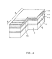
- Fig. 3 shows a DBR semiconductor laser device in accordance with a second embodiment of the present invention.
- the diffraction grating 6a is formed only at a distributed reflection region B of the diffraction grating layer 6.
- the method for manufacturing this structure is the same as for the first embodiment up to the formation of the p-type Ga 0.8 Al 0.2 As diffraction grating layer 6 in the first crystal growth process.
- the diffraction grating 6a is formed only in the distributed reflection region B by etching only the distributed reflection region B and not the active region A in the surface of the diffraction grating layer 6.
- the length of the active region was set to 500 ⁇ m
- the length of the distributed reflection region was set to 300 ⁇ m.
- a second optical guiding layer 7, an etch-stop layer 8, and a current blocking layer 9 are formed.
- a window 9a serving as a current channel has been etched into the current blocking layer 9
- a p-type second cladding layer 10 and a p-type GaAs contact layer 11 are grown.
- the p-type GaAs contact layer 11 is eliminated by etching over a width of 30 ⁇ m between the active region A and the distributed reflection region B. Then, an n-type electrode 21 is formed on the GaAs substrate 1 and a p-type electrode 22 is formed on the p-type GaAs contact layer of the active region A, thereby completing the semiconductor laser device shown in Fig. 3.
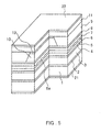
- Fig. 5 shows a DBR semiconductor laser device in accordance with a third embodiment of the present invention.
- the second cladding layer 10 is provided with a ridge shape, and for current confinement, an n-type Ga 0.4 Al 0.6 As current blocking layer 9 is formed in the region outside the ridge serving as a current channel.
- Numeral 12 denotes a p-type GaAs protective layer, and numeral 11 denotes a p-type GaAs contact layer.
- FIG. 6 A method for manufacturing this semiconductor laser is shown in Fig. 6. First, as in the first and second embodiments, the layers up to the diffraction grating layer are formed in a first crystal growth process, then the diffraction grating 6A is formed, and the layers up to the protective layer 12 are formed in a second crystal growth process, as shown in Fig. 6A.
- a stripe-shaped dielectric film 13 for example of nitride (silicon nitride or tungsten nitride) or silicon oxide, is formed, and etching is performed using this dielectric film 13 as a mask, forming a ridge. The etching is stopped selectively with the etch-stop layer 8.
- an n-type Ga 0.4 Al 0.6 As current blocking layer 9 is grown selectively in the region outside the ridge in a third crystal growth process, as shown in Fig. 6C.
- a regular mesa shape is preferable to an inverted mesa shape for the ridge shape, because with the inverted mesa shape, crystal growth is more difficult than with the regular mesa shape, which may reduce the yield.
- a p-type GaAs contact layer 11 is formed in a fourth crystal growth process.
- an n-type electrode 21 is formed on the n-type GaAs substrate 1 and a p-type electrode 22 is formed on the p-type GaAs contact layer 11, thereby completing the semiconductor laser device shown in Fig. 5.
- Fig. 7 shows a DBR semiconductor laser device in accordance with a fourth embodiment of the present invention.
- the second cladding layer 10 is provided with a ridge shape, and for current confinement, an n-type Ga 0.4 Al 0.6 As current blocking layer 9 is formed in the region outside the ridge serving as a current channel.
- the diffraction grating 6a is formed only in the distributed reflection region B of the diffraction grating layer 6.
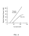
- Fig. 8 is a graph showing the current - optical output characteristics of a semiconductor laser in accordance with an embodiment of the present invention.
- a current reduction is accomplished. Due to this current reduction, the element's generation of heat during high output power can be suppressed, and a stable oscillation in single longitudinal mode can be attained even at output powers of 100mW or higher. Moreover, stable oscillation with a single transverse mode is possible up to high output powers.
- the threshold can be reduced by providing the active layer with a quantum well structure, so that the current can be reduced and the output power can be increased. If multiple quantum wells of 10nm thickness Ga 0.95 Al 0.05 As well layers and 4nm thick Ga 0.7 Al 0.3 As barrier layers are used for the quantum well structure for oscillation in the 780nm band, then an optical output of 200mW or more can be attained.
- Fig. 9 shows a DBR semiconductor laser device in accordance with the present invention.
- the period of the diffraction grating is an integer multiple of the wavelength in the medium.
- a third cladding layer 38 of p-type Ga 0.5 Al 0.5 As is formed on the current blocking layer 37, and a contact layer 39 of p-type GaAs is formed on top of that.
- An active region 40 is formed adjacent to the distributed Bragg reflection region 41.
- the diffraction grating 37b is formed in the current blocking layer 37 with the striped-shaped window 37a and serves as the distributed Bragg reflection region 41, so that the DBR laser structure is accomplished simply by forming the third cladding layer 38 and the contact layer 39 on top of the current blocking layer 37. That is to say, it takes only two crystal growth processes to manufacture the DBR laser structure on the semiconductor substrate 31. In other words, the crystal growth for manufacturing the DBR laser is interrupted only once, so that the DBR laser structure can be manufactured with high yield.
- the diffraction grating is formed on the current blocking layer 37, and the laser light leaks into the current blocking layer 37 where it is propagated, so that the coupling coefficient of the diffraction grating can be made large.
- a DBR laser with high emission wavelength selectivity can be obtained.
- the forbidden band width of the second optical guiding layer 37 of n-type Ga 0.4 Al 0.6 As is larger than the forbidden band width of the active layer 34 of Ga 0.85 Al 0.15 As, so that there is almost no optical absorbtion in the current blocking layer 37, and a DBR laser with low operating current and low waveguide losses can be obtained.
- the current injected from the contact layer 39 of p-type GaAs is confined in the stripe-shaped window 37a, and a laser oscillation in the 780nm band occurs in the active layer 34 of Ga 0.85 Al 0.15 As below the stripe-shaped window 37a.
- the forbidden band of the second cladding layer 35 of p-type Ga 0.5 Al 0.5 As is sufficiently larger than that in the active layer 34 of Ga 0.85 Al 0.15 As, and the carriers are confined effectively in the active layer 34, so that oscillation in the visual spectrum is possible.
- the AlAs crystal composition ratio should be set to at least about 0.35, and in the present embodiment it was set to 0.5.
- the forbidden band of the current blocking layer 37 is also larger than the forbidden band of the third cladding layer 38, so that the current can be confined effectively to the stripe-shaped window 37a.
- the refractive index in the medium that is, in the waveguide, changes periodically, and light advancing in parallel to the resonator direction is periodically reflected.
- the diffraction grating 37b has a period that is an integer multiple of the wavelength in the medium, and the light reflected by the diffraction grating 37b is coherent, so that the wavelength selectivity is increased.
- single longitudinal mode oscillation can be maintained with greater stability towards temperature changes, variations in optical output power, and high-speed modulation.
- Fig. 10 illustrates a method for manufacturing this semiconductor laser.
- a buffer layer 32 of n-type GaAs, a first cladding layer 33 of n-type Ga 0.5 Al 0.5 As, an active layer 34 of Ga 0.85 Al 0.15 As, a second cladding layer 35 of p-type Ga 0.5 Al 0.5 As, a grating layer 36 of p-type Ga 0.8 Al 0.2 As, and a current blocking layer 37 of n-type Ga 0.4 Al 0.6 As are formed in that order on a substrate 31 of n-type GaAs by organic gas-phase metal epitaxial growth (MOCVD) or molecular beam epitaxy (MBE),
- MOCVD organic gas-phase metal epitaxial growth
- MBE molecular beam epitaxy
- a stripe-shaped window 37a is formed by etching in the current blocking layer 37.
- the current blocking layer 37 of n-type Ga 0.4 Al 0.6 As is etched with an etchant with almost no selectivity towards the AlAs crystal composition ratio, such as sulfuric acid, and then the current blocking layer 37 is selectively etched with an etchant with high selectivity towards the AlAs crystal composition ratio, such as a hydrofluoric acid or phosphoric acid system.
- the grating layer 36 of p-type Ga 0.8 Al 0.2 As acts as an etch-stop layer.
- a diffraction grating was patterned in the resist film, and a diffraction grating 37b was formed by etching in the grating layer 36 and the current blocking layer 37 of the distributed Bragg reflection region 41.
- a third cladding layer 38 of p-type Ga 0.5 Al 0.5 As and a contact layer 39 of p-type GaAs were formed by regrowing with MOCVD or MBE.
- electrodes were formed on the semiconductor substrate 31 of n-type GaAs and the contact layer 39 of p-type GaAs.
- a diffraction grating 37b is formed in the current blocking layer 37, so that after the diffraction grating 37b has been formed, the DBR laser structure can be manufactured without interrupting the crystal growth. Therefore, the manufacturing yield for the DBR laser can be increased.
- the conductivity type of the active layer 34 is not particularly specified, and it can be p-type, n-type or undoped.
- this embodiment has been explained for a semiconductor substrate 31 of n-type GaAs and a current blocking layer 37 of n-type Ga 0.4 Al 0.6 As, but it is also possible to use a semiconductor substrate 31 of p-type GaAs and a p-type current blocking layer 37. Since the forbidden band of the current blocking layer 37 is large, electron scattering can be suppressed, and a p-type current blocking layer can be realized with a p-type GaAlAs layer with a large forbidden band, that is, with high AlAs crystal composition ratio.
Landscapes
- Physics & Mathematics (AREA)
- Condensed Matter Physics & Semiconductors (AREA)
- General Physics & Mathematics (AREA)
- Electromagnetism (AREA)
- Optics & Photonics (AREA)
- Geometry (AREA)
- Semiconductor Lasers (AREA)
Abstract
Description
Claims (17)
- A semiconductor laser device, comprising:a substrate;an active layer formed on the substrate;a semiconductor layer provided with a diffraction grating formed on the active layer;an etch-stop layer formed on the semiconductor layer;a cladding layer provided with a stripe structure, formed on the etch-stop layer; anda current blocking layer formed on the etch-stop layer and arranged at least on the sides of said stripe structure.
- The semiconductor laser device according to Claim 1, wherein the refractive index of the current blocking layer is lower than the refractive index of the cladding layer.
- The semiconductor laser device according to Claim 1, wherein the stripe-shaped structure is of regular mesa shape.
- The semiconductor laser device according to Claim 1, wherein the etch-stop layer is a Ga1-SAlSAs layer of a first conductivity type, the current blocking layer is a Ga1-ZAlZAs layer of a second conductivity type, the cladding layer is a Ga1-CAlCAs layer of the first conductivity type, and the relation between C, S, and Z is 1 ≧ Z > C > S ≧ 0.
- The semiconductor laser device according to Claim 4, further comprising a first optical guiding layer of Ga1-Y1AlY1As (0 < Y1 < 1) of the first conductivity type between the active layer and the diffraction grating layer.
- The semiconductor laser device according to Claim 4, further comprising a second optical guiding layer of Ga1-Y2AlY2As (0 < Y2 < 1) of the first conductivity type between the semiconductor layer with the diffraction grating and the etch-stop layer, wherein the semiconductor layer is a layer of Ga1-GAlGAs (0 ≦ G ≦ 1), and the relation between G and Y2 is Y2 > G.
- The semiconductor laser device according to Claim 4, wherein the active layer has a quantum well structure including well layers made of Ga1- xAlxAs (0 ≦ X < 1).
- The semiconductor laser device according to Claim 1, wherein the semiconductor layer with the diffraction grating comprises a region at which the diffraction grating is formed and a region at which the diffraction grating is not formed.
- The semiconductor laser device according to Claim 1, wherein the diffraction grating is formed at least near an end face in the semiconductor layer with the diffraction grating.
- A method for manufacturing the semiconductor laser device as claimed in any one of Claims 1 to 9, comprising:forming an etch-stop layer of Ga1-SAlSAs;forming an etched layer of Ga1-UAlUAs (with 1 ≧ U > S ≧ 0) selected from the cladding layer and the current blocking layer; andforming a stripe structure by etching this etched layer with an etchant that selectively etches GaAlAs layers with higher Al ratio.
- The method for manufacturing a semiconductor according to Claim 10, wherein the etchant is hydrofluoric acid.
- A distributed Bragg reflection semiconductor laser device, comprising:a substrate;an active layer formed on the substrate; anda current blocking layer formed on the active layer and having a stripe-shaped window;wherein a diffraction grating is formed at least near an end face in the current blocking layer.
- The semiconductor laser device according to Claim 12, wherein grooves forming the diffraction grating are arranged along a longitudinal direction of the stripe-shaped window.
- The semiconductor laser device according to Claim 12, wherein the period of the diffraction grating is an integer multiple of the wavelength of light that can propagate through its medium.
- The semiconductor laser device according to Claim 12, wherein a forbidden band width of the current blocking layer is larger than a forbidden band width of the active layer.
- The semiconductor laser device according to Claim 12, further comprising a cladding layer formed on the stripe-shaped window, wherein a forbidden band width of the current blocking layer is larger than a forbidden band width of the cladding layer.
- A method for manufacturing the distributed Bragg reflection semiconductor laser device as claimed in any one of Claims 12 to 16, comprising:forming the current blocking layer on the active layer;partially removing the current blocking layer to form the stripe-shaped window; andforming the diffraction grating at least in a region of the current blocking layer that is near an end face.
Applications Claiming Priority (4)
| Application Number | Priority Date | Filing Date | Title |
|---|---|---|---|
| JP2000055291 | 2000-03-01 | ||
| JP2000055291A JP2001244558A (en) | 2000-03-01 | 2000-03-01 | Semiconductor laser device and method of manufacturing the same |
| JP2000100304A JP2001284713A (en) | 2000-04-03 | 2000-04-03 | Distributed Bragg reflection semiconductor laser and method of manufacturing the same |
| JP2000100304 | 2000-04-03 |
Publications (2)
| Publication Number | Publication Date |
|---|---|
| EP1130723A2 true EP1130723A2 (en) | 2001-09-05 |
| EP1130723A3 EP1130723A3 (en) | 2004-03-24 |
Family
ID=26586493
Family Applications (1)
| Application Number | Title | Priority Date | Filing Date |
|---|---|---|---|
| EP01301871A Withdrawn EP1130723A3 (en) | 2000-03-01 | 2001-03-01 | Semiconductor laser device and method for manufacturing the same |
Country Status (3)
| Country | Link |
|---|---|
| US (1) | US7050472B2 (en) |
| EP (1) | EP1130723A3 (en) |
| TW (1) | TW480797B (en) |
Families Citing this family (3)
| Publication number | Priority date | Publication date | Assignee | Title |
|---|---|---|---|---|
| JP5073186B2 (en) * | 2005-08-24 | 2012-11-14 | ローム株式会社 | Monolithic semiconductor laser |
| JP2012227332A (en) * | 2011-04-19 | 2012-11-15 | Sumitomo Electric Ind Ltd | Ridge type semiconductor laser and method for manufacturing the same |
| US10475962B2 (en) * | 2017-02-15 | 2019-11-12 | Epistar Corporation | Optoelectronic device |
Family Cites Families (11)
| Publication number | Priority date | Publication date | Assignee | Title |
|---|---|---|---|---|
| JPS6066484A (en) | 1983-09-22 | 1985-04-16 | Toshiba Corp | Manufacture of semiconductor laser device |
| JPH01186688A (en) * | 1987-09-02 | 1989-07-26 | Sharp Corp | Semiconductor laser device |
| JPH0719931B2 (en) | 1989-04-06 | 1995-03-06 | 三菱電機株式会社 | Semiconductor laser device and manufacturing method thereof |
| EP0475714B1 (en) * | 1990-09-10 | 1995-12-27 | Sharp Kabushiki Kaisha | A distributed feedback semiconductor laser device and a method of producing the same |
| JP3274710B2 (en) | 1991-07-24 | 2002-04-15 | シャープ株式会社 | Distributed feedback semiconductor laser device and method of manufacturing distributed feedback semiconductor laser device |
| DE69220303T2 (en) | 1991-07-24 | 1998-01-02 | Sharp Kk | Process for the production of a semiconductor laser with distributed feedback |
| JP3242967B2 (en) * | 1992-01-31 | 2001-12-25 | 株式会社東芝 | Semiconductor light emitting device |
| JP3040262B2 (en) | 1992-09-29 | 2000-05-15 | 松下電子工業株式会社 | Semiconductor laser device |
| JPH0955558A (en) * | 1995-08-11 | 1997-02-25 | Sharp Corp | Semiconductor laser device |
| JP3710524B2 (en) | 1995-08-31 | 2005-10-26 | シャープ株式会社 | Ridge waveguide type distributed feedback semiconductor laser device and manufacturing method thereof |
| CA2249053A1 (en) | 1997-09-30 | 1999-03-30 | Mitsui Chemicals, Incorporated | Semiconductor laser device |
-
2001
- 2001-02-28 US US09/795,959 patent/US7050472B2/en not_active Expired - Lifetime
- 2001-03-01 TW TW090104674A patent/TW480797B/en not_active IP Right Cessation
- 2001-03-01 EP EP01301871A patent/EP1130723A3/en not_active Withdrawn
Also Published As
| Publication number | Publication date |
|---|---|
| US20010019567A1 (en) | 2001-09-06 |
| TW480797B (en) | 2002-03-21 |
| US7050472B2 (en) | 2006-05-23 |
| EP1130723A3 (en) | 2004-03-24 |
Similar Documents
| Publication | Publication Date | Title |
|---|---|---|
| EP0788203A1 (en) | Semiconductor laser device | |
| KR20010007396A (en) | Semiconductor laser | |
| JP3381534B2 (en) | Self-oscillation type semiconductor laser | |
| JP3204474B2 (en) | Gain-coupled distributed feedback semiconductor laser and its fabrication method | |
| US20040013144A1 (en) | Complex-coupled distributed feedback semiconductor laser device | |
| JP2002353559A (en) | Semiconductor laser and method of manufacturing the same | |
| JP2003069144A (en) | Distributed feedback semiconductor laser device | |
| JP5310533B2 (en) | Optical semiconductor device | |
| JP3932466B2 (en) | Semiconductor laser | |
| US7050472B2 (en) | Semiconductor laser device and method for manufacturing the same | |
| EP1089407A1 (en) | Gain-coupled distributed-feedback semiconductor laser device | |
| US6856636B2 (en) | Semiconductor laser device | |
| JPH0770785B2 (en) | Distributed reflection type semiconductor laser | |
| JP2842465B2 (en) | Semiconductor laser device and method of manufacturing the same | |
| JPH06188509A (en) | Semiconductor light emitting element and fabrication thereof | |
| JP2613975B2 (en) | Periodic gain type semiconductor laser device | |
| JP2009076640A (en) | Semiconductor light emitting device | |
| JP3040262B2 (en) | Semiconductor laser device | |
| JP2723921B2 (en) | Semiconductor laser device | |
| JP2004134486A (en) | Semiconductor laser equipped with diffraction grating | |
| JP2783163B2 (en) | Distributed feedback semiconductor laser and method of manufacturing the same | |
| JPH09246664A (en) | Semiconductor laser | |
| JPH06283801A (en) | Semiconductor laser | |
| JP3277711B2 (en) | Semiconductor laser and manufacturing method thereof | |
| RU2272344C2 (en) | Semiconductor laser unit generating high-power radiation (alternatives) and its manufacturing process |
Legal Events
| Date | Code | Title | Description |
|---|---|---|---|
| PUAI | Public reference made under article 153(3) epc to a published international application that has entered the european phase |
Free format text: ORIGINAL CODE: 0009012 |
|
| AK | Designated contracting states |
Kind code of ref document: A2 Designated state(s): AT BE CH CY DE DK ES FI FR GB GR IE IT LI LU MC NL PT SE TR |
|
| AX | Request for extension of the european patent |
Free format text: AL;LT;LV;MK;RO;SI |
|
| PUAL | Search report despatched |
Free format text: ORIGINAL CODE: 0009013 |
|
| AK | Designated contracting states |
Kind code of ref document: A3 Designated state(s): AT BE CH CY DE DK ES FI FR GB GR IE IT LI LU MC NL PT SE TR |
|
| AX | Request for extension of the european patent |
Extension state: AL LT LV MK RO SI |
|
| AKX | Designation fees paid | ||
| REG | Reference to a national code |
Ref country code: DE Ref legal event code: 8566 |
|
| STAA | Information on the status of an ep patent application or granted ep patent |
Free format text: STATUS: THE APPLICATION IS DEEMED TO BE WITHDRAWN |
|
| 18D | Application deemed to be withdrawn |
Effective date: 20040924 |