EP1130645A2 - Semiconductor chip with a thermal stress relief layer on the electrodes - Google Patents
Semiconductor chip with a thermal stress relief layer on the electrodes Download PDFInfo
- Publication number
- EP1130645A2 EP1130645A2 EP01104798A EP01104798A EP1130645A2 EP 1130645 A2 EP1130645 A2 EP 1130645A2 EP 01104798 A EP01104798 A EP 01104798A EP 01104798 A EP01104798 A EP 01104798A EP 1130645 A2 EP1130645 A2 EP 1130645A2
- Authority
- EP
- European Patent Office
- Prior art keywords
- plate
- thermal stress
- molybdenum
- plates
- element body
- Prior art date
- Legal status (The legal status is an assumption and is not a legal conclusion. Google has not performed a legal analysis and makes no representation as to the accuracy of the status listed.)
- Withdrawn
Links
Images



Classifications
-
- H—ELECTRICITY
- H10—SEMICONDUCTOR DEVICES; ELECTRIC SOLID-STATE DEVICES NOT OTHERWISE PROVIDED FOR
- H10D—INORGANIC ELECTRIC SEMICONDUCTOR DEVICES
- H10D18/00—Thyristors
- H10D18/80—Bidirectional devices, e.g. triacs
-
- H—ELECTRICITY
- H10—SEMICONDUCTOR DEVICES; ELECTRIC SOLID-STATE DEVICES NOT OTHERWISE PROVIDED FOR
- H10D—INORGANIC ELECTRIC SEMICONDUCTOR DEVICES
- H10D99/00—Subject matter not provided for in other groups of this subclass
-
- H—ELECTRICITY
- H10—SEMICONDUCTOR DEVICES; ELECTRIC SOLID-STATE DEVICES NOT OTHERWISE PROVIDED FOR
- H10D—INORGANIC ELECTRIC SEMICONDUCTOR DEVICES
- H10D62/00—Semiconductor bodies, or regions thereof, of devices having potential barriers
- H10D62/10—Shapes, relative sizes or dispositions of the regions of the semiconductor bodies; Shapes of the semiconductor bodies
- H10D62/117—Shapes of semiconductor bodies
-
- H—ELECTRICITY
- H10—SEMICONDUCTOR DEVICES; ELECTRIC SOLID-STATE DEVICES NOT OTHERWISE PROVIDED FOR
- H10W—GENERIC PACKAGES, INTERCONNECTIONS, CONNECTORS OR OTHER CONSTRUCTIONAL DETAILS OF DEVICES COVERED BY CLASS H10
- H10W40/00—Arrangements for thermal protection or thermal control
- H10W40/20—Arrangements for cooling
- H10W40/25—Arrangements for cooling characterised by their materials
- H10W40/255—Arrangements for cooling characterised by their materials having a laminate or multilayered structure, e.g. direct bond copper [DBC] ceramic substrates
-
- H—ELECTRICITY
- H10—SEMICONDUCTOR DEVICES; ELECTRIC SOLID-STATE DEVICES NOT OTHERWISE PROVIDED FOR
- H10W—GENERIC PACKAGES, INTERCONNECTIONS, CONNECTORS OR OTHER CONSTRUCTIONAL DETAILS OF DEVICES COVERED BY CLASS H10
- H10W40/00—Arrangements for thermal protection or thermal control
- H10W40/20—Arrangements for cooling
- H10W40/25—Arrangements for cooling characterised by their materials
- H10W40/258—Metallic materials
-
- H—ELECTRICITY
- H10—SEMICONDUCTOR DEVICES; ELECTRIC SOLID-STATE DEVICES NOT OTHERWISE PROVIDED FOR
- H10W—GENERIC PACKAGES, INTERCONNECTIONS, CONNECTORS OR OTHER CONSTRUCTIONAL DETAILS OF DEVICES COVERED BY CLASS H10
- H10W72/00—Interconnections or connectors in packages
- H10W72/30—Die-attach connectors
-
- H—ELECTRICITY
- H10—SEMICONDUCTOR DEVICES; ELECTRIC SOLID-STATE DEVICES NOT OTHERWISE PROVIDED FOR
- H10W—GENERIC PACKAGES, INTERCONNECTIONS, CONNECTORS OR OTHER CONSTRUCTIONAL DETAILS OF DEVICES COVERED BY CLASS H10
- H10W76/00—Containers; Fillings or auxiliary members therefor; Seals
- H10W76/10—Containers or parts thereof
- H10W76/12—Containers or parts thereof characterised by their shape
- H10W76/13—Containers comprising a conductive base serving as an interconnection
- H10W76/138—Containers comprising a conductive base serving as an interconnection having another interconnection being formed by a cover plate parallel to the conductive base, e.g. sandwich type
-
- H—ELECTRICITY
- H10—SEMICONDUCTOR DEVICES; ELECTRIC SOLID-STATE DEVICES NOT OTHERWISE PROVIDED FOR
- H10W—GENERIC PACKAGES, INTERCONNECTIONS, CONNECTORS OR OTHER CONSTRUCTIONAL DETAILS OF DEVICES COVERED BY CLASS H10
- H10W72/00—Interconnections or connectors in packages
- H10W72/071—Connecting or disconnecting
- H10W72/073—Connecting or disconnecting of die-attach connectors
-
- H—ELECTRICITY
- H10—SEMICONDUCTOR DEVICES; ELECTRIC SOLID-STATE DEVICES NOT OTHERWISE PROVIDED FOR
- H10W—GENERIC PACKAGES, INTERCONNECTIONS, CONNECTORS OR OTHER CONSTRUCTIONAL DETAILS OF DEVICES COVERED BY CLASS H10
- H10W72/00—Interconnections or connectors in packages
- H10W72/071—Connecting or disconnecting
- H10W72/073—Connecting or disconnecting of die-attach connectors
- H10W72/07331—Connecting techniques
- H10W72/07336—Soldering or alloying
-
- H—ELECTRICITY
- H10—SEMICONDUCTOR DEVICES; ELECTRIC SOLID-STATE DEVICES NOT OTHERWISE PROVIDED FOR
- H10W—GENERIC PACKAGES, INTERCONNECTIONS, CONNECTORS OR OTHER CONSTRUCTIONAL DETAILS OF DEVICES COVERED BY CLASS H10
- H10W72/00—Interconnections or connectors in packages
- H10W72/071—Connecting or disconnecting
- H10W72/075—Connecting or disconnecting of bond wires
-
- H—ELECTRICITY
- H10—SEMICONDUCTOR DEVICES; ELECTRIC SOLID-STATE DEVICES NOT OTHERWISE PROVIDED FOR
- H10W—GENERIC PACKAGES, INTERCONNECTIONS, CONNECTORS OR OTHER CONSTRUCTIONAL DETAILS OF DEVICES COVERED BY CLASS H10
- H10W72/00—Interconnections or connectors in packages
- H10W72/30—Die-attach connectors
- H10W72/351—Materials of die-attach connectors
- H10W72/352—Materials of die-attach connectors comprising metals or metalloids, e.g. solders
-
- H—ELECTRICITY
- H10—SEMICONDUCTOR DEVICES; ELECTRIC SOLID-STATE DEVICES NOT OTHERWISE PROVIDED FOR
- H10W—GENERIC PACKAGES, INTERCONNECTIONS, CONNECTORS OR OTHER CONSTRUCTIONAL DETAILS OF DEVICES COVERED BY CLASS H10
- H10W72/00—Interconnections or connectors in packages
- H10W72/30—Die-attach connectors
- H10W72/381—Auxiliary members
-
- H—ELECTRICITY
- H10—SEMICONDUCTOR DEVICES; ELECTRIC SOLID-STATE DEVICES NOT OTHERWISE PROVIDED FOR
- H10W—GENERIC PACKAGES, INTERCONNECTIONS, CONNECTORS OR OTHER CONSTRUCTIONAL DETAILS OF DEVICES COVERED BY CLASS H10
- H10W72/00—Interconnections or connectors in packages
- H10W72/50—Bond wires
- H10W72/531—Shapes of wire connectors
- H10W72/5363—Shapes of wire connectors the connected ends being wedge-shaped
-
- H—ELECTRICITY
- H10—SEMICONDUCTOR DEVICES; ELECTRIC SOLID-STATE DEVICES NOT OTHERWISE PROVIDED FOR
- H10W—GENERIC PACKAGES, INTERCONNECTIONS, CONNECTORS OR OTHER CONSTRUCTIONAL DETAILS OF DEVICES COVERED BY CLASS H10
- H10W72/00—Interconnections or connectors in packages
- H10W72/50—Bond wires
- H10W72/551—Materials of bond wires
- H10W72/552—Materials of bond wires comprising metals or metalloids, e.g. silver
- H10W72/5524—Materials of bond wires comprising metals or metalloids, e.g. silver comprising aluminium [Al]
-
- H—ELECTRICITY
- H10—SEMICONDUCTOR DEVICES; ELECTRIC SOLID-STATE DEVICES NOT OTHERWISE PROVIDED FOR
- H10W—GENERIC PACKAGES, INTERCONNECTIONS, CONNECTORS OR OTHER CONSTRUCTIONAL DETAILS OF DEVICES COVERED BY CLASS H10
- H10W72/00—Interconnections or connectors in packages
- H10W72/50—Bond wires
- H10W72/59—Bond pads specially adapted therefor
-
- H—ELECTRICITY
- H10—SEMICONDUCTOR DEVICES; ELECTRIC SOLID-STATE DEVICES NOT OTHERWISE PROVIDED FOR
- H10W—GENERIC PACKAGES, INTERCONNECTIONS, CONNECTORS OR OTHER CONSTRUCTIONAL DETAILS OF DEVICES COVERED BY CLASS H10
- H10W72/00—Interconnections or connectors in packages
- H10W72/851—Dispositions of multiple connectors or interconnections
- H10W72/874—On different surfaces
- H10W72/884—Die-attach connectors and bond wires
-
- H—ELECTRICITY
- H10—SEMICONDUCTOR DEVICES; ELECTRIC SOLID-STATE DEVICES NOT OTHERWISE PROVIDED FOR
- H10W—GENERIC PACKAGES, INTERCONNECTIONS, CONNECTORS OR OTHER CONSTRUCTIONAL DETAILS OF DEVICES COVERED BY CLASS H10
- H10W72/00—Interconnections or connectors in packages
- H10W72/90—Bond pads, in general
- H10W72/951—Materials of bond pads
- H10W72/952—Materials of bond pads comprising metals or metalloids, e.g. PbSn, Ag or Cu
-
- H—ELECTRICITY
- H10—SEMICONDUCTOR DEVICES; ELECTRIC SOLID-STATE DEVICES NOT OTHERWISE PROVIDED FOR
- H10W—GENERIC PACKAGES, INTERCONNECTIONS, CONNECTORS OR OTHER CONSTRUCTIONAL DETAILS OF DEVICES COVERED BY CLASS H10
- H10W90/00—Package configurations
- H10W90/701—Package configurations characterised by the relative positions of pads or connectors relative to package parts
- H10W90/731—Package configurations characterised by the relative positions of pads or connectors relative to package parts of die-attach connectors
- H10W90/736—Package configurations characterised by the relative positions of pads or connectors relative to package parts of die-attach connectors between a chip and a stacked lead frame, conducting package substrate or heat sink
Definitions
- the present invention relates to a chip-type semiconductor device. More particularly, the present invention relates to a chip-type semiconductor device having an element body, an electrode provided on at least one surface of the element body, and a thermal stress cushioning plate provided on the electrode by interposing an alloy plate made of aluminum and silicon.
- Fig. 7 illustrates an arrangement of a TRIAC which is a typical example of such chip-type semiconductor device.
- This TRIAC has electrodes 11 and 12 on one surface (upper surface in Fig. 7) of an element body 10 made of silicon and an electrode 13 on the other surface (lower surface in Fig. 7).
- a molybdenum plate 30 is provided as a thermal stress cushioning plate by a high-temperature (melting point of about 290°C) solder layer 20.
- a molybdenum plate 31 is provided as a thermal stress cushioning plate by a high-temperature solder layer 21.
- the molybdenum plate 30 is secured to an outer electrode plate (T1 terminal) 40 made of copper by a low-temperature (melting point of about solder 180°C) layer 25, and the molybdenum plate 31 is secured to an outer electrode plate (T2 terminal) 41 made of copper by a low-temperature layer 26, and a wire (gate lead) 45 made of aluminum is bonded to the electrode 11.
- the molybdenum plates 30 and 31 are employed for preventing application of thermal stress to the element body 10, the thermal stress being caused by difference between thermal expansion coefficient of the outer electrode plates 40 and 41 and thermal expansion coefficient of the element body 10 made of silicon.
- the low-temperature solder is used for connecting the chip-type semiconductor device to the outer electrode plates 40 and 41.
- the composition of the low-temperature is Pb: 38% and Sn: 62%, for example.
- new low-temperature solder is going to be produced commercially instead the above low-temperature solder, but the melting point of the new low-temperature solder is increased, i.e. 240 ⁇ 250°C.
- the high-temperature solder is used for adhering silicon (element body 10) and molybdenum (molybdenum plates 30 and 31).
- the composition of the high-temperature solder is Pb: 92.5%, Ag: 2.5%, and In: 5%, for example.
- the Pb content is remarkably great for increasing the adhesion force of the both by increasing viscosity. It is a great issue how to deal or improve or the like the high-temperature solder, especially. But, no effective measure is taken at all under the present condition.
- the melting point of the low-temperature solder used by a user is not sufficiently lower than that of the high-temperature solder which is used for the chip-type semiconductor, the high-temperature solder layers 20 and 21 of the chip-type semiconductor device are melted easily by the heat generated by soldering when the chip-type semiconductor device is connected to the outer electrode plates 40 and 41.
- the substitute of the above low-temperature solder is high in melting point such as 240 ⁇ 250 °C. Therefore, when such substitute is employed, adhesive agent having higher melting point should be employed instead the conventional adhesive agent for adhering the element body 10 and the molybdenum plates 30 and 31. It is difficult for developing such adhesive agent having a high melting point.
- the molybdenum plates 30 and 31 cannot sufficiently realize thermal stress cushioning effect which is the essential characteristic, because the molybdenum plates 30 and 31 and the element body 10 are adhered by the high-temperature solder layers 20 and 21. Therefore, the expansion quantity of solder is directly applied to the element body 10 in real so that the thermal stress life of the element body 10 is directly influenced badly.
- the present invention was made in view of the conventional problems.
- a chip-type semiconductor device comprises an element body, an electrode provided on at least one surface of the element body, a thermal stress cushioning plate, and an alloy plate made of aluminum and silicon for connecting the electrode and the thermal stress cushioning plate.
- the alloy plate employed in the chip-type semiconductor device is made of aluminum and silicon, and includes no harmful lead, so that the chip-type semiconductor is in sufficient conformity with the home electric device recycle law and the like. Further, the alloy plate is made of aluminum and silicon, so that not only the silicon consisting semiconductor device and the alloy plate but also the alloy plate and the thermal stress cushioning plate (having a thermal expansion coefficient which is similar to that of silicon) made of molybdenum, tungsten, covar and the like are simultaneously and firmly connected.
- a eutectic temperature of the alloy plate may vary to some degree depending upon components content rate but is greatly lower than the melting point of 240 ⁇ 250°C of the above low-temperature solder substitute, no problems arise when the substitute is used for connecting the semiconductor device and the outer electrode plate. Further, the thermal stress cushioning operation of the thermal stress cushioning plate is sufficiently realized so as to lengthen thermal stress life of the element body, because the thermal stress cushioning plate and the element body are connected without the high-temperature solder.
- a composition rate of the alloy plate is aluminum content of 87 ⁇ 89% and silicon content of 11 ⁇ 13%. Within this extent, it is most preferable in operations and effects that the alloy plate has the composition rate is aluminum content of 88% and silicon content of 12% so that the eutectic temperature becomes extremely high temperature of about 580°C.
- the chip-type semiconductor device includes all power semiconductors or the like such as diode, transistor, thyrister, TRIAC, IGBT and the like.
- Material of the thermal stress cushioning plate is exemplified as molybdenum, tungsten, covar and the like.
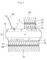
- Fig. 1 illustrates an arrangement of a TRIAC which is an embodiment of a chip-type semiconductor device.
- This TRIAC has an arrangement which is the same to that of the TRIAC illustrated in Fig. 7 excepting that alloy plates 1 and 2, and nickel layers 3 and 4 are provided and that the electrode 13 is not necessary. That is, this TRIAC includes an element body 10 made of silicon, and electrodes 11 and 12 made of aluminum on one surface (upper surface in Fig. 1) of the element body 10.
- a molybdenum plate 30 as a thermal stress cushioning plate is provided to the electrode 12 by an alloy plate 1 made of aluminum and silicon, for example.
- a molybdenum plate 31 is provided to the other surface (lower surface in Fig. 1) of the element body 10 by an alloy plate 2 which is similar to the alloy plate 1.
- nickel layers 3 and 4 are provided on connection face of the molybdenum plates 30 and 31 to the outer electrode plates 40 and 41.
- the element body 10 is constituted with a plurality of N-layer and P-layer, and comer sections of the element body 10 are covered by glass 15.
- the electrodes 11 and 12 are made by deposition of aluminum.
- the nickel layers 3 and 4 are used for making soldering easily when a user employs low-temperature solder.
- the nickel layers 3 and 4 may be nickel clad (made by sticking a nickel plate and a molybdenum plate) or may be formed by nickel plating.
- the molybdenum plate 30 is connected to the outer electrode plate (T1 terminal) 40 made of copper by solder 27, and the molybdenum plate 31 is connected to the outer electrode plate (T2 terminal) 41 made of copper by solder 28, and a wire (gate lead) 45 made of aluminum is bonded to the electrode 11.
- the solder 27 and 28 may be conventional low-temperature solder or may be the above low-temperature solder substitute.
- the low-temperature solder substitute has a high melting point of 240 ⁇ 250°C, but the eutectic temperature of the alloy plates 1 and 2 is about 580°C and is greatly higher than the melting point, therefore no problems arise and generality is improved.
- the molybdenum plates 30 and 31 are provided by alloy plates 1 and 2 made of aluminum and silicon, so that not only silicon constituting the element body 10 and the alloy plates 1 and 2 but also the alloy plates 1 and 2 and the molybdenum plates 30 and 31 can be simultaneously and firmly connected, and thermal contraction (temperature cycle) characteristic is greatly improved.
- the alloy plates 1 and 2 are employed, a eutectic alloy layer is formed in the element body 10 by aluminum which is one component of the alloy plates 1 and 2, so that ohmic characteristic of the element body 10 is improved.
- the TRIAC is in conformity with the home electric device recycle law and the like, because the alloy plates 1 and 2 do not include noxious element such as lead and the like. Further, the thermal stress cushioning operation of the molybdenum plates 30 and 31 is sufficiently realized so as to lengthen the thermal stress life of the element body 10.
- the molybdenum plates 30 and 31 are connected to the element body 10 by the alloy plates 1 and 2, the element body 10, the alloy plates 1 and 2, and the molybdenum plates 30 and 31 are put within a hydrogen reducing furnace under the condition that the alloy plates 1 and 2 are put between the element body 10 and the molybdenum plates 30 and 31, heat processing with temperature of 680°C is carried out for about 15 minutes, so that the molybdenum plates 30 and 31 are provided to the element body 10 by interposing the alloy plates 1 and 2.
- the usage of the hydrogen reducing furnace is for preventing oxidation of the alloy plates 1 and 2 and the like.
- heat processing can be performed with temperature lower than 680°C, and adherence to the alloy (Al/Si) plate is improved.
- ambient atmosphere of the heat processing is not limited to hydrogen ambient atmosphere. Alloying processing (heat processing) can be performed within N 2 (Nitrogen) ambient atmosphere.
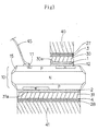
- Fig. 2 illustrates an arrangement of a TRIAC which is a chip-type semiconductor device of another embodiment.
- Fig. 3 illustrates an arrangement of a TRIAC which is a chip-type semiconductor device of a further embodiment.
- This TRIAC has an arrangement which is the same to the arrangement of the TRIAC illustrated in Fig. 1, fundamentally.
- This TRIAC is different from the TRIAC illustrated in Fig. 1 in that connection faces of the molybdenum plates 30 and 31 to the alloy plates 1 and 2 are formed to be rough surfaces 30a and 31a.
- connection faces of the molybdenum plates 30 and 31 to the alloy plates 1 and 2 are formed to be rough surfaces 30a and 31a.
- contacting area to the alloy plates 1 and 2 substantially increase so as to improve connection strength of the molybdenum plates 30 and 31 and the alloy plates 1 and 2.
- Specific example of the rough surfaces 30a and 31a is exemplified as wave shaped face, saw-tooth shaped face, rectangular tooth shaped face, irregular unevenness face and the like.
- the shape of the rough surfaces 30a and 31a is not limited to the above shapes as long as the connection area of the molybdenum plates 30 and 31 and the alloy plates 1 and 2 is increased.
- the TRIAC of each of the above embodiments is merely an example.
- a TRIAC can be applied the optimum designing corresponding to a usage so as to realize high reliance and high function.
- the size of the thermal stress cushioning plate can be applied the optimum designing in accordance with the shape of the user-side outer electrode plate and the heat capacity. That is, the thermal stress cushioning plate is enlarged when the outer electrode plate is great, while the thermal stress cushioning plate is made to have a small size when the outer electrode plate is small.
- the T1 electrode 12 of the element body 10 is increased its area, as is illustrated in Fig. 4 (arrangement figure), in Fig.
- the T1 electrode 12 is formed by aluminum deposition layer (thickness: ⁇ 10 ⁇ m).
- a TRIAC is employed as an example of a chip-type semiconductor device.
- operations and effects are realized which are similar to those of the above embodiments.
Landscapes
- Thyristors (AREA)
- Die Bonding (AREA)
Abstract
Description
Claims (4)
- A chip-type semiconductor device including an electrode (11, 12) on at least one face of an element body (10), and a thermal stress cushioning plate (30) provided on the electrode (12) by a solder layer,
the device is characterized in that
an alloy plate (1) made of aluminum and silicon is employed instead the solder layer. - A chip-type semiconductor device as set forth in claim 1, wherein the alloy plate (1) has the component content of aluminum: 87 ∼ 89% and silicon: 11 ∼ 13%.
- A chip-type semiconductor as set forth in claim 1 or claim 2, wherein the thermal stress cushioning plate (30) has a rough surface (30a)on its connection side to the alloy plate (12).
- A chip-type semiconductor device as set forth in one of claims 1 ∼ 3, wherein the thermal stress cushioning plate (30) has a nickel layer (3)on its connection face to an outer electrode (40).
Applications Claiming Priority (2)
| Application Number | Priority Date | Filing Date | Title |
|---|---|---|---|
| JP2000052699 | 2000-02-29 | ||
| JP2000052699 | 2000-02-29 |
Publications (2)
| Publication Number | Publication Date |
|---|---|
| EP1130645A2 true EP1130645A2 (en) | 2001-09-05 |
| EP1130645A3 EP1130645A3 (en) | 2003-10-01 |
Family
ID=18574171
Family Applications (1)
| Application Number | Title | Priority Date | Filing Date |
|---|---|---|---|
| EP01104798A Withdrawn EP1130645A3 (en) | 2000-02-29 | 2001-02-27 | Semiconductor chip with a thermal stress relief layer on the electrodes |
Country Status (4)
| Country | Link |
|---|---|
| US (1) | US6614105B2 (en) |
| EP (1) | EP1130645A3 (en) |
| KR (1) | KR100499722B1 (en) |
| TW (1) | TW492196B (en) |
Cited By (1)
| Publication number | Priority date | Publication date | Assignee | Title |
|---|---|---|---|---|
| EP2075835A3 (en) * | 2007-12-28 | 2010-01-13 | Robert Bosch Gmbh | Diode with stress reducing means |
Families Citing this family (3)
| Publication number | Priority date | Publication date | Assignee | Title |
|---|---|---|---|---|
| EP1403923A1 (en) * | 2002-09-27 | 2004-03-31 | Abb Research Ltd. | Press pack power semiconductor module |
| DE10352670A1 (en) * | 2003-11-11 | 2005-06-16 | eupec Europäische Gesellschaft für Leistungshalbleiter mbH | Electric component with equaliser of temperature caused mechanical stresses, connecting two part-elements with different length expansion coefficients, e.g. for optical components, i.e. glass plate connected to copper electrode etc |
| US7897452B2 (en) * | 2005-06-20 | 2011-03-01 | Fuji Electric Systems Co., Ltd. | Method of producing a semiconductor device with an aluminum or aluminum alloy rear electrode |
Family Cites Families (9)
| Publication number | Priority date | Publication date | Assignee | Title |
|---|---|---|---|---|
| DE1803489A1 (en) * | 1968-10-17 | 1970-05-27 | Siemens Ag | Method for manufacturing a semiconductor component |
| US3925808A (en) * | 1974-08-08 | 1975-12-09 | Westinghouse Electric Corp | Silicon semiconductor device with stress-free electrodes |
| JPS53117966A (en) * | 1977-03-25 | 1978-10-14 | Toshiba Corp | Semiconductor device |
| US4358784A (en) * | 1979-11-30 | 1982-11-09 | International Rectifier Corporation | Clad molybdenum disks for alloyed diode |
| DE3421672A1 (en) * | 1984-06-09 | 1985-12-12 | SEMIKRON Gesellschaft für Gleichrichterbau u. Elektronik mbH, 8500 Nürnberg | INTERCHANGEABLE RESISTANT, SWITCHABLE SEMICONDUCTOR COMPONENT |
| DE69018846T2 (en) * | 1989-02-10 | 1995-08-24 | Fujitsu Ltd | Semiconductor device type ceramic package and method of assembling the same. |
| US4921158A (en) * | 1989-02-24 | 1990-05-01 | General Instrument Corporation | Brazing material |
| JP2705689B2 (en) * | 1996-04-12 | 1998-01-28 | 三菱マテリアル株式会社 | Method of manufacturing lightweight substrate for semiconductor device |
| US6033787A (en) * | 1996-08-22 | 2000-03-07 | Mitsubishi Materials Corporation | Ceramic circuit board with heat sink |
-
2001
- 2001-02-26 KR KR10-2001-0009747A patent/KR100499722B1/en not_active Expired - Lifetime
- 2001-02-27 TW TW090104506A patent/TW492196B/en not_active IP Right Cessation
- 2001-02-27 EP EP01104798A patent/EP1130645A3/en not_active Withdrawn
- 2001-02-28 US US09/794,629 patent/US6614105B2/en not_active Expired - Lifetime
Cited By (1)
| Publication number | Priority date | Publication date | Assignee | Title |
|---|---|---|---|---|
| EP2075835A3 (en) * | 2007-12-28 | 2010-01-13 | Robert Bosch Gmbh | Diode with stress reducing means |
Also Published As
| Publication number | Publication date |
|---|---|
| US6614105B2 (en) | 2003-09-02 |
| EP1130645A3 (en) | 2003-10-01 |
| KR100499722B1 (en) | 2005-07-07 |
| US20010017377A1 (en) | 2001-08-30 |
| KR20010085616A (en) | 2001-09-07 |
| TW492196B (en) | 2002-06-21 |
Similar Documents
| Publication | Publication Date | Title |
|---|---|---|
| US6891265B2 (en) | Semiconductor device having radiation structure | |
| KR101194429B1 (en) | Semiconductor device and method for producing the same | |
| US8044523B2 (en) | Semiconductor device | |
| US6803667B2 (en) | Semiconductor device having a protective film | |
| US8164176B2 (en) | Semiconductor module arrangement | |
| JP3271475B2 (en) | Electrical element joining material and joining method | |
| US20040102023A1 (en) | Semiconductor device and method of relaxing thermal stress | |
| JP4014652B2 (en) | Semiconductor device assembly and circuit | |
| EP2587532A2 (en) | Joined structural body of members, joining method of members, and package for containing an electronic component | |
| US8110437B2 (en) | Method for attaching a semiconductor chip in a plastic encapsulant, optoelectronic semiconductor component and method for the production thereof | |
| EP0460785B1 (en) | Semiconductor device having a heat sink | |
| US12027490B2 (en) | Semiconductor device and method for fabricating the same | |
| US6512304B2 (en) | Nickel-iron expansion contact for semiconductor die | |
| US4057825A (en) | Semiconductor device with composite metal heat-radiating plate onto which semiconductor element is soldered | |
| JPH11265976A (en) | Power semiconductor module and method of manufacturing the same | |
| US6614105B2 (en) | Chip-type semiconductor device | |
| JPH10135377A (en) | Mold type semiconductor device | |
| JP2003133329A (en) | Semiconductor device | |
| CN115398608A (en) | Semiconductor device with a plurality of transistors | |
| US5483105A (en) | Module input-output pad having stepped set-back | |
| US20240312896A1 (en) | Semiconductor device | |
| JP3446829B2 (en) | Semiconductor device | |
| EP4300571A1 (en) | Power semiconductor module arrangement and method for forming the same | |
| US20230369166A1 (en) | Power semiconductor module arrangement and method for producing the same | |
| JPH07202060A (en) | Chip carrier |
Legal Events
| Date | Code | Title | Description |
|---|---|---|---|
| PUAI | Public reference made under article 153(3) epc to a published international application that has entered the european phase |
Free format text: ORIGINAL CODE: 0009012 |
|
| 17P | Request for examination filed |
Effective date: 20010323 |
|
| AK | Designated contracting states |
Kind code of ref document: A2 Designated state(s): AT BE CH CY DE DK ES FI FR GB GR IE IT LI LU MC NL PT SE TR |
|
| AX | Request for extension of the european patent |
Free format text: AL;LT;LV;MK;RO;SI |
|
| PUAL | Search report despatched |
Free format text: ORIGINAL CODE: 0009013 |
|
| AK | Designated contracting states |
Kind code of ref document: A3 Designated state(s): AT BE CH CY DE DK ES FI FR GB GR IE IT LI LU MC NL PT SE TR |
|
| AX | Request for extension of the european patent |
Extension state: AL LT LV MK RO SI |
|
| 17Q | First examination report despatched |
Effective date: 20040416 |
|
| AKX | Designation fees paid |
Designated state(s): AT BE CH CY DE DK ES FI FR GB GR IE IT LI LU MC NL PT SE TR |
|
| STAA | Information on the status of an ep patent application or granted ep patent |
Free format text: STATUS: THE APPLICATION IS DEEMED TO BE WITHDRAWN |
|
| 18D | Application deemed to be withdrawn |
Effective date: 20051215 |