EP1128570A2 - Echo compensator for telecommunication systems - Google Patents
Echo compensator for telecommunication systems Download PDFInfo
- Publication number
- EP1128570A2 EP1128570A2 EP00125584A EP00125584A EP1128570A2 EP 1128570 A2 EP1128570 A2 EP 1128570A2 EP 00125584 A EP00125584 A EP 00125584A EP 00125584 A EP00125584 A EP 00125584A EP 1128570 A2 EP1128570 A2 EP 1128570A2
- Authority
- EP
- European Patent Office
- Prior art keywords
- signal
- echo
- line
- compensation
- circuit
- Prior art date
- Legal status (The legal status is an assumption and is not a legal conclusion. Google has not performed a legal analysis and makes no representation as to the accuracy of the status listed.)
- Withdrawn
Links
Images


Classifications
-
- H—ELECTRICITY
- H04—ELECTRIC COMMUNICATION TECHNIQUE
- H04B—TRANSMISSION
- H04B3/00—Line transmission systems
- H04B3/02—Details
- H04B3/20—Reducing echo effects or singing; Opening or closing transmitting path; Conditioning for transmission in one direction or the other
- H04B3/23—Reducing echo effects or singing; Opening or closing transmitting path; Conditioning for transmission in one direction or the other using a replica of transmitted signal in the time domain, e.g. echo cancellers
Definitions
- the present invention relates generally to the field of data communications and in particular to a circuit and method for compensating for transmission echo in a telecommunications system.
- Data communication systems are commonly used to transmit and/or receive data between remote transmitting and receiving locations.
- a central facet of any data communications system is the reliability and integrity of the data communicated.
- the data, received at the receiving location is identical to the data transmitted from the transmitting location.
- transmission echo i.e., reflection of the transmitted signal such that it appears as part of the received signal
- the effects of transmission echo can cause the data which is being received to be corrupted or lost.
- Signals received by a modem typically have a large dynamic range and may be affected by transmission echo.
- echo has a greater effect on modem performance.
- a broadband Digital Subscriber Line (xDSL) operating over twisted pair copper wires such as Asymmetric Digital Subscriber Line (ADSL) technology, uses signals transmitted at up to and over two megahertz which are typically attenuated by as much as 90 dB before being received by the modem.
- the upstream and downstream data channels may use overlapping frequencies. When overlapping frequencies are used, the modem transmission echo must be compensated for, as it will have a greater amplitude than the received signal in the same frequency spectrum.
- ADSL systems the frequency spectrum is assigned to the various communications channels conveyed over the twisted pair using a splitter. The lowest 4kHz of bandwidth is reserved for use by analog devices such as common telephones of the baseband Plain Old Telephone Service (POTS).
- POTS Plain Old Telephone Service
- a medium frequency range full duplex channel in the frequency range of 30 kHz to 140 kHz may be defined to carry upstream ADSL data and downstream ADSL data having a typical data rate in the 16 kbps to 640 kbps range.
- a high frequency channel that uses frequencies in the 140kHz to 1104 kHz range carries downstream data having a typical data rate in the 1.536 Mbps to 6.144 Mbps range. Accordingly, the medium frequency upstream and downstream data channels used by ADSL modems may use overlapping frequency ranges.
- Modems and other communication systems typically include a hybrid coupling circuit for connecting to the local loop which then connects to the telephone company central office.
- the transmitted and received signals may be transmitted on overlapping frequencies as in the case of ADSL. Accordingly, an ADSL modem must incorporate a suitable hybrid circuit to attenuate or compensate for its own transmission echo in order to maximize the dynamic range of the receive path of the ADSL modem.
- the received signal is detected at the secondary side (the side of the transformer connected to the modem and hybrid circuit) of the line transformer.
- the transmitted echo signal (which has had its characteristics affected by the line transformer and the line itself) is inseparable from the received signal at the secondary side of the line transformer.
- the transmitted echo signal may oftentimes be affected by the telephone company central office devices, requiring compensation by the line compensation circuit of the balanced hybrid circuit.
- a sample of the transmitted signal is taken from the output of the modem line driver and this sample is processed in order to obtain a replica of the transmitted echo signal.
- the replica of the transmitted echo signal is then subtracted from the received signal. Accordingly, the effectiveness of the attenuation of the transmission echo signal is related to how well the reconstructed echo signal matches the actual transmission echo signal. Accordingly, the received signal has an improved received to transmit echo signal ratio when the echo compensation circuit of the hybrid circuit closely replicates the transmission echo.
- Prior art hybrids and circuits used to compensate for transmission echo signals in modems have several disadvantages, such as the use of a large number of components. Additional disadvantages of prior art devices include the use of active circuitry for transmission echo reconstruction and subtraction that can increase distortion and nonlinearity.
- the invention relates to a balanced hybrid coupling circuit and method of using the hybrid in a full duplex modem device to attenuate the transmission echo of the modem when receiving a signal from another communications device over a communications channel such as common telephone lines.
- the balanced hybrid coupling circuit of the present invention receives a differential transmission signal from a pair of differential drivers in the modem.
- a line transformer couples the differential transmit signal to the local loop twisted pair copper cable.
- the received signal from the far end is received on the same local loop twisted pair copper cable and is also coupled to the modem receiver by the line transformer.
- the transmit signal is sampled, e.g., across a sampling resistor, and subtracted from the line signal to reconstruct the received signal.
- the modem transmission will create an echo signal due to the effects of the line transformer and local loop
- the present invention will simultaneously sample the transmitted signal across two RC networks that respectively simulate the effects of the line transformer and the local loop. These RC networks produce components of a transmission echo signal replica that are also subtracted from the line signal to more accurately isolate the received signal which is then supplied to the differential receiver in the modem.
- the first RC network of each half of the balanced hybrid circuit is used to compensate for the transmission echo effect of the line transformer by simulating the transmission echo effect of the line transformer and producing a component of a transmission echo replica signal that approximates the transmission echo produced by the line transformer.
- the sample is effectively inverted by actually sampling the transmission signal of the opposite transmitter of the differential transmitter pair.
- the transmission echo replica signal component is subtracted from the line signal to isolate the received signal.
- the second RC network of each half of the balanced hybrid circuit is used to compensate for the transmission echo effect of the line or local loop twisted pair copper wire by simulating the transmission echo effect of the line and producing a component of a transmission echo replica signal that approximates the transmission echo produced by the line.
- the transmission echo replica signal component is subtracted from the line signal to further isolate the received signal.
- the balanced hybrid coupling circuit of the present invention transmits and receives a differential signal through a line transformer.
- the echo compensation hybrid circuit creates a replica of the transmission echo signal and subtracts the echo replica signal along with the transmitted signal from the line to obtain the true received signal.
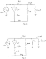
- the differential transmission signals 1,3 are received at the two respective line drivers 2,4.
- the transmission signals are sampled by the respective sampling resistors Rs1, Rs2 at the output of the line drivers 2, 4 and coupled to the line 16 by line transformer 14 .
- the sampled transmission signal is input to the echo compensation circuit 12 which produces a compensated received signal 18.
- the transmit portion of the simplified hybrid circuit includes a transmitted signal source Vtx in series with a sampling resistor Rs1 and a load resistor Rload which equals the resistance of the line 16 transformed to the secondary winding of the transformer.
- the parameter "return loss” is a measure of how close the modem output impedance matches a reference impedance, which is defined as 100 Ohms in the standard specification for an ADSL modem. High return loss is an advantageous characteristic of a modem, indicating a proper impedance match.
- the sample resistor Rs1 is chosen to equal the load resistance value Rload.
- FIG. 3 therein is illustrated a single ended (unbalanced) simplification of the hybrid circuit shown in FIG. 1 that is used to describe the echo compensation for the real component of the load reflected through the transformer 14 .
- FIG. 3 illustrates a simplification assuming an ideal transformer 14 and a constant Ohmic impedance for line 16.
- the line 16 is assumed to have a very large attenuation that masks the influence of the impedance of any modem or other communications device connected to the other end of the line 16 .
- a current limiting resistor R32 is placed between the Vload node and the Vrx node.
- the resistor R32 has a value chosen to be much greater than the value of Rs1 so that it does not significantly load the Vload node.
- resistor R36 of the simplified circuit corresponds to resistor R74 in the final balanced hybrid compensation circuit of FIG.8 as part of the RC network which compensates for the echo effect of the transformer 14 .
- FIG. 4 therein is illustrated a single ended (unbalanced) simplification of the hybrid circuit shown in FIG. 1 that is used to describe the echo compensation for the effect of the secondary winding of a real transformer.
- FIG. 4 illustrates a simplification assuming that the transformer 14 is not an ideal transformer, but rather a non-ideal transformer 14 with a secondary inductance L and a constant Ohmic impedance Rload for line 16.
- the inductance L of the transformer is simplified as an inductance connected in parallel with Rload . Accordingly, to compensate for the effect of the line transformer 14 secondary inductance L, the sample of Vtx that is subtracted from Vrx is modified by capacitor C .
- the inductor L affects Vload by adding a zero at the origin and a pole at the frequency that corresponds to the RL time constant of L and the parallel combination of Rs1 and Rload .
- the sample is taken from the complementary transmission signal. Accordingly the compensating sample should have a signal with the same amplitude, but with opposite polarity.
- the capacitor C of the simplified circuit corresponds to capacitor C78 in the final balanced hybrid compensation circuit of FIG. 8 as part of the RC network which compensates for the echo effect of the transformer 14.
- FIG. 5 therein is illustrated a simplification of the input impedance of the twisted pair local loop line 16.
- An actual twisted pair line has a characteristic impedance that is complex and is a function of the frequency of the transmitted and received signals.
- the simple model of such an impedance is shown in FIG 5, and includes Rline1 in series with the parallel combination of Rline2 and Cline.
- the characteristic impedance ofthe local loop twisted pair copper wire varies according to the physical parameters such as the distance from the telephone company central office, wire gauge and number of twists per inch. Accordingly, there are differences in line impedance in different countries and as between different lines in a country.
- a regulatory agency of a country may specify a line impedance value required of the telephone company and in such instance the value of a typical line impedance is known a priori. Additionally, the line 16 is assumed to have attenuation that masks the influence of the impedance of the equipment at the other end of the line 16. If a communications device attached to the other end of line 16 has an impedance influence that is not negligible, the impedance of the line 16 can be modeled to consider such communications device impedance.
- FIG. 6 therein is illustrated a single ended (unbalanced) simplification of the transmit circuit shown in FIG. 1, similar to the simplification shown in FIG 2, but instead having a complex load impedance Zload .
- the magnitude of the load impedance decreases as the frequency increases. Therefore, to compensate for the effect of the line impedance on the transmission signal Vtx , the Vtx sample will be processed to provide an echo replica signal that compensates for the frequency dependance of the line impedance.
- the replica signal will be created using a second RC network as described below.
- FIG. 7 therein is illustrated a single ended (unbalanced) hybrid circuit having two RC branches which compensate for the transmission echo effect of the line impedance and line transformer, respectively.
- the first RC network of each half of the balanced hybrid circuit is used to compensate for the transmission echo effect of the line transformer and includes resistor R74 in series with capacitor C78 as described above with reference to FIGs. 2-4.
- the second RC network of each half of the balanced hybrid circuit is used to compensate for the transmission echo effect of the line or local loop twisted pair copper wire and includes resistor R72 in series with capacitor C76 as described above with reference to FIGs. 5 and 6.
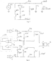
- FIG. 8 therein is illustrated a complete schematic diagram of the balanced hybrid echo compensation circuit.
- the inverter 34 that is used in FIG. 7 to denote a connection to the complementary circuit is not used in Fig. 8 because the actual connection between node Vrx and C78 and the connection between node - Vrx and C78' are shown.
- the balanced hybrid coupling circuit receives a differential transmission signal from a pair of differential drivers 2,4 .
- the line transformer 14 couples the differential transmission signal output by the line drivers 2,4 through sampling resistors Rs1, and Rs2 and then to the local loop twisted pair copper cable line 16.
- the hybrid receives a signal that is transmitted on the same local loop twisted pair copper cable line 16 and is also coupled to the modem receiver by the line transformer 14 .
- the following description relates to one half of the balanced hybrid, but as can be appreciated, the other half of the circuit denoted with prime values in FIG. 8 operates in an identical manner.
- the transmit signal itself must first be subtracted. This is achieved by sampling the transmit signal across a sampling resistor Rs1 through current limiting resistor R32 . Resistor R32 has a much greater value than Rs1 in order to minimize any loading effect.
- the sampled transmit signal is subtracted from the line signal to create the received signal isolated from the transmission signal on the local loop. Because the modem transmission also creates an echo signal due to the effects of the line transformer 14 and local loop line 16, the hybrid circuit simultaneously samples the transmitted signal Vtx across two RC networks R72, C76 and R74, C78 which respectively simulate the effect of the line transformer and the local loop. These RC networks produce components of a transmission echo signal replica that are also subtracted from the line signal to further isolate the received signal Vrx which is then supplied to the differential receiver 82 in the modem.
- the first RC network the line transformer compensation circuit.
- R74, C78 having resistor R74 and capacitor C78 , is used to compensate for the transmission echo effect of the line transformer, by simulating the transmission echo effect of the line transformer and producing a component of a transmission echo replica signal that approximates the transmission echo produced by the line transforme 14 .
- the sample is effectively inverted by actually sampling the transmission signal - Vtx of the opposite transmitter of the differential transmitter pair.
- the transmission echo replica signal component is subtracted from the line signal to isolate the received signal Vrx .
- the second RC network the line compensation circuit, R72, C76 having resistor R72 and capacitor C76 , is used to compensate for the transmission echo effect of the line (or local loop twisted pair copper wire and any non-negligible communication device effect) 16 , by simulating the transmission echo effect of the line 16 and producing a component of a transmission echo replica signal that approximates the transmission echo produced by the line.
- the transmission echo replica signal component is subtracted from the line signal to further isolate the received signal Vrx.
- the effect of the telephone company central office devices or other devices connected to the ADSL modem is not negligible, that effect can be compensated for by modifying the balanced hybrid circuit.
- the effect of any other device connected to the line can be compensated by including their electrical models at the final stage of the balanced hybrid circuit design when the balanced hybrid circuit components are optimized.
- a typical line impedance table is shown below. The line impedance table could be modified to include the electrical characteristic of any other device connected to the line.
- the component values of the balanced hybrid circuit can then be optimized to provide optimal echo compensation using commercially available circuit optimization software such as the "Super Star” package available from Eagleware Corporation.
- R32 should be much larger than Rs1 for minimal loading of the transmitted signal.
- the transformer inductance L is chosen according to the lowest working frequency to minimize its attenuation at the lowest working frequency and to obtain adequate frequency matching at the lowest frequency used in order to achieve a high return loss as usually required by relevant industry and government standards.
- the resistor R74 is selected such that the resistance value is lower than the value of R72 because the current through resistor R74 is the main hybrid signal injection route.
- the signal current injected through resistor R72 has a lower value than that through R74 so that it lowers the total signal current injected into node Vrx by injecting a smaller current with reverse polarity. Accordingly, R72 has a higher resistance value than R74.
- the critical frequency of the transformer compensation RC network, R74, C78 is selected such that it is lower than the critical frequency of the line compensation RC network, R72, C76 such that the former influences the hybrid operation at the transformer cutoff frequency at the lowest working frequency.
- the line compensation RC network, R72, C76 affects the signal injection at a higher frequency where it compensates for the impedance change of the line with varying frequency.
- resistor R74 is selected such that it is twice the resistance of R32 so that the voltage at node Vtx is approximately twice the voltage as at Vload . Accordingly, to achieve adequate rejection of the transmission signal Vtx at node Vrx, R74 should be approximately twice as large as R32 as described above in relation to the analysis of the circuit simplification shown in Figure 3.
- the first current path includes the first RC network R74, C78 which compensates for the transmission echo effect of the line transformer.
- the second current path includes the second RC network R72, C76 which compensates for the transmission echo effect of the local loop and can at all frequencies used be made to inject a current of the same magnitude with opposite polarity into the received signal node Vrx , thereby achieving a high transmission signal and transmission echo signal rejection from the received signal path.
- the echo signal current into node Vrx is canceled as described below.
- the received signal is a signal that is injected from the line 16 to the input of the balanced hybrid coupling circuit at node Vload and injects signal current into node Vrx through resistor R32.
- the other hybrid branches do not inject any received signal current into node Vrx because the other hybrid branches are connected at the output of the Transmission signal line driver 2 that has an output impedance of zero. Accordingly, only the transmission signal Vtx exists at the output of the Transmission signal line driver 2 and there is no received signal cancellation through the other hybrid branches.
- the balanced hybrid coupling circuit of the present invention advantageously utilizes a circuit topology with a relatively small number of components.
- the present invention may utilize passive components in the transmission echo reconstruction circuit in order to maximize linearity of the signals processed and minimize distortion.
- the present invention may also utilize passive components in the subtraction circuit. Accordingly, only the subtracted signal with the enhanced receive to transmit signal ratio enters the receive path amplifiers, thus minimizing distortion and maximizing the dynamic range of the receiver.
- the present invention provides compensation for the transmission echo signal component produced by the line transformer.
- the present invention may also compensate for a high pass filter incorporated into the line transformer or connected to the line transformer by modeling the impedance of that filter as part of the load impedance.
- a simple RC network of the balanced hybrid circuit provides sufficiently effective echo compensation only when there is relatively slow variation of the line impedance and phase.
- High pass filters have a higher rate of change of impedance and phase as the order of the filter increases.
- a third order high pass filter can be compensated from frequencies slightly above the critical frequency and above. As the order of the filter is increased, the frequency ranges compensated for will be much higher than the critical frequency and it will be a less effective hybrid circuit.
- the present invention may compensate for the transmission echo effect of up to a third order line high pass filter which can include series capacitors at the primary (line side) and secondary (modem and hybrid side) of the transformer.
- the present invention may utilize the connection of two series RC branches that are connected between low impedance points, which cancels the interaction between the branches such that a change to one branch will not affect the other branch.
- the system and method of the present invention are implemented in any number of communications or other related schemes where full duplex transmission over overlapping frequencies require the compensation for transmission echo signals, e.g., in embedded telecommunications systems, modems, and other wire-line and non-wireline signal transfer applications.
- the system may be implemented in embedded applications or as part of a larger data communications system.
Landscapes
- Engineering & Computer Science (AREA)
- Computer Networks & Wireless Communication (AREA)
- Signal Processing (AREA)
- Cable Transmission Systems, Equalization Of Radio And Reduction Of Echo (AREA)
- Telephonic Communication Services (AREA)
Abstract
Description
| Frequency (MHz) | Z (Ohm) | Phase (Deg.) |
| .005 | 301.2 | -280.8 |
| .01 | 220.6 | -191.8 |
| .015 5 | 186.5 | -151.5 |
| .02 | 167 | -126.8 |
| .025 | 154.5 | -109.9 |
| .03 | 145.7 | -97.4 |
| .035 | 139.2 | -87.5 |
| .04 | 134.3 | -79.6 |
| .05 | 127.3 | -67.5 |
| .06 | 122.5 | -58.7 |
| .07 | 119.2 | -52 |
| .08 | 116.8 | -46.8 |
| .09 | 115 | -42.6 |
| .1 | 113.6 | -39.1 |
| .12 | 111.5 | -33.8 |
| .14 | 110.1 | -29.9 |
| .16 | 109.2 | -26.9 |
| .18 | 108.4 | -24.6 |
| .2 | 107.8 | -22.8 |
| .25 | 106.7 | -19.5 |
| .3 | 105.9 | -17.3 |
| .4 | 104.8 | -14.6 |
| .5 | 103.9 | -12.9 |
| .6 | 103.1 | -11.7 |
| .7 | 102.5 | -10.9 |
| .8 | 101.9 | -10.2 |
| 1.0 | 100.9 | -9.1 |
Claims (11)
- A method for correcting for an echo signal component in a telecommunications device, comprising the steps of:sampling a transmitted signal across a sampling resistor;subtracting the sampled transmitted signal from a received line signal to obtain a reconstructed received signal;sampling the transmitted signal across a first RC network echo compensation circuit to obtain a first echo compensation signal; andsubtracting the first echo compensation signal from the received line signal to compensate the reconstructed received signal.
- The method of claim 1, further comprising the steps of:sampling the transmitted signal across a second RC network echo compensation circuit to obtain a second echo compensation signal: andsubtracting the second echo compensation signal from the received line signal to compensate the reconstructed received signal.
- The method of claim 1, further comprising the steps of:sampling a second transmitted signal across a second sampling resistor;subtracting the second sampled transmitted signal from a second received line signal to obtain a second reconstructed received signal;sampling the second transmitted signal across a second RC network echo compensation circuit to obtain a second echo compensation signal; andsubtracting the second echo compensation signal from the second received line signal to compensate the second reconstructed received signal.
- The method of claim 3, further comprising the steps of:sampling the transmitted signal across a third RC network echo compensation circuit to obtain a third echo compensation signal;subtracting the third echo compensation signal from the second received line signal to compensate the second reconstructed received signal;sampling the second transmitted signal across a fourth RC network echo compensation circuit to obtain a fourth echo compensation signal; andsubtracting the fourth echo compensation signal from the received line signal to compensate the reconstructed received signal.
- An apparatus for compensating for echo signal in a telecommunications device comprising:a transmitter having an output;a receiver having an input;a line transformer coupled to the transmitter output and the receiver input; andan echo compensation circuit including a first circuit branch coupled to the transmitter output and the receiver input and a second circuit branch coupled to the transmitter output and the receiver input.
- The apparatus according to claim 5, wherein:the first circuit branch further comprises a first resistor and a first capacitor connected in series; andthe second circuit branch further comprises a second resistor and a second capacitor connected in series.
- The apparatus according to claim 6, further comprisinga second transmitter having an output;a second receiver having an input; anda second echo compensation circuit including a third circuit branch coupled to the second transmitter output and the second receiver input and a fourth circuit branch coupled to the transmitter output,wherein the line transformer is coupled to the second transmitter output and the second receiver input; andwherein the second circuit branch is coupled to the transmitter output and the second receiver input.
- The apparatus according to claim 7, wherein:the third circuit branch further comprises a third resistor and a third capacitor connected in series; andthe fourth circuit branch further comprises a fourth resistor and a fourth capacitor connected in series.
- An apparatus for compensating for echo signal in a telecommunications device comprising:a first differential transmitter having an output terminal coupled to a first transmitted signal node;a second differential transmitter having an output terminal coupled to a second transmitted signal node;a first current limiting resistor having a first terminal coupled to the first transmitted signal node and a second terminal coupled to a first line transformer node;a second current limiting resistor having a first terminal coupled to the second transmitted signal node and a second terminal coupled to a second line transformer node;a first sampling resistor having a first terminal coupled to the first line transformer node and a second terminal connected to a first received signal node;a second sampling resistor having a first terminal coupled to the second line transformer node and a second terminal connected to a second received signal node;a first compensation circuit having a first terminal coupled to the first transmitted signal node and a second terminal coupled to the first received signal node;a second compensation circuit having a first terminal coupled to the first transmitted signal node and a second terminal coupled to the second received signal node;a third compensation circuit having a first terminal coupled to the second transmitted signal node and a second terminal coupled to the second received signal node; anda fourth compensation circuit having a first terminal coupled to the second transmitted signal node and a second terminal coupled to the first received signal node.
- An apparatus for compensating for echo signal in a telecommunications device according to claim 9 wherein,the first compensation circuit further comprises a first compensation resistor and a first compensation capacitor connected in series;the second compensation circuit further comprises a second compensation resistor and a second compensation capacitor connected in series;the third compensation circuit further comprises a third compensation resistor and a third compensation capacitor connected in series; andthe fourth compensation circuit further comprises a fourth compensation resistor and a fourth compensation capacitor connected in series.
- An apparatus for compensating for echo signal in a telecommunications device according to claim 9 wherein,the first terminal of the first sampling resistor is coupled to the first transmitted signal node; andthe first terminal of the second sampling resistor is coupled to the second transmitted signal node.
Applications Claiming Priority (2)
| Application Number | Priority Date | Filing Date | Title |
|---|---|---|---|
| US09/460,891 US6956944B1 (en) | 1999-12-14 | 1999-12-14 | Method and apparatus for compensating for an echo signal component in telecommunication systems |
| US460891 | 1999-12-14 |
Publications (2)
| Publication Number | Publication Date |
|---|---|
| EP1128570A2 true EP1128570A2 (en) | 2001-08-29 |
| EP1128570A3 EP1128570A3 (en) | 2002-02-20 |
Family
ID=23830471
Family Applications (1)
| Application Number | Title | Priority Date | Filing Date |
|---|---|---|---|
| EP00125584A Withdrawn EP1128570A3 (en) | 1999-12-14 | 2000-11-22 | Echo compensator for telecommunication systems |
Country Status (2)
| Country | Link |
|---|---|
| US (1) | US6956944B1 (en) |
| EP (1) | EP1128570A3 (en) |
Cited By (3)
| Publication number | Priority date | Publication date | Assignee | Title |
|---|---|---|---|---|
| EP1612962A1 (en) * | 2004-06-29 | 2006-01-04 | Infineon Technologies AG | Broadband xDSL transceiver |
| CN101436881A (en) * | 2007-11-14 | 2009-05-20 | 美国博通公司 | Hybrid circuit without inductors |
| DE102005004369B4 (en) * | 2005-01-31 | 2010-09-16 | Infineon Technologies Ag | Method and device for echo compensation of a received signal |
Families Citing this family (5)
| Publication number | Priority date | Publication date | Assignee | Title |
|---|---|---|---|---|
| US7170927B2 (en) * | 2002-08-16 | 2007-01-30 | Texas Instruments Incorporated | Methods and apparatus for an ADSL transceiver |
| US7030679B2 (en) * | 2004-07-29 | 2006-04-18 | Elantec Semiconductor, Inc. | Analog multiplexing circuits |
| US7684499B2 (en) * | 2005-08-30 | 2010-03-23 | 2Wire, Inc. | Multi-band line interface circuit with line side cancellation |
| US9032355B2 (en) | 2013-10-03 | 2015-05-12 | Helic S.A. | System and method for integrated transformer synthesis and optimization using constrained optimization problem |
| US12058083B2 (en) * | 2020-11-12 | 2024-08-06 | Avago Technologies International Sales Pte. Limited | Capacitive hybrid with PGA for full duplex transceivers |
Family Cites Families (8)
| Publication number | Priority date | Publication date | Assignee | Title |
|---|---|---|---|---|
| JPS5614734A (en) * | 1979-07-18 | 1981-02-13 | Nippon Telegr & Teleph Corp <Ntt> | Two-wire handset |
| GB2123259A (en) * | 1982-06-25 | 1984-01-25 | Philips Electronic Associated | Digital duplex communication system |
| JPH01180126A (en) * | 1988-01-11 | 1989-07-18 | Nec Corp | Echo canceller |
| JP2898165B2 (en) * | 1993-04-16 | 1999-05-31 | シャープ株式会社 | Hybrid circuit |
| EP0693846A3 (en) | 1994-06-24 | 1999-05-26 | Harris Corporation | Telephone subscriber line interface circuit and method |
| US5912924A (en) * | 1996-08-15 | 1999-06-15 | Seeq Technology, Inc. | Bidirectional channels using common pins for transmit and receive paths |
| US6542604B1 (en) * | 1998-08-31 | 2003-04-01 | Infineon Technologies Ag | Scaled impedance replica for echo attenuation in digital transmission systems |
| US6445791B1 (en) * | 1999-08-09 | 2002-09-03 | Cirrus Logic, Inc. | System and methods for modem interface |
-
1999
- 1999-12-14 US US09/460,891 patent/US6956944B1/en not_active Expired - Lifetime
-
2000
- 2000-11-22 EP EP00125584A patent/EP1128570A3/en not_active Withdrawn
Cited By (7)
| Publication number | Priority date | Publication date | Assignee | Title |
|---|---|---|---|---|
| EP1612962A1 (en) * | 2004-06-29 | 2006-01-04 | Infineon Technologies AG | Broadband xDSL transceiver |
| DE102005004369B4 (en) * | 2005-01-31 | 2010-09-16 | Infineon Technologies Ag | Method and device for echo compensation of a received signal |
| CN101436881A (en) * | 2007-11-14 | 2009-05-20 | 美国博通公司 | Hybrid circuit without inductors |
| EP2061158A1 (en) * | 2007-11-14 | 2009-05-20 | Broadcom Corporation | Hybrid circuit without inductors |
| US8315378B2 (en) | 2007-11-14 | 2012-11-20 | Broadcom Corporation | Hybrid circuit without inductors |
| TWI403104B (en) * | 2007-11-14 | 2013-07-21 | Broadcom Corp | Hybrid circuit without inductors |
| CN101436881B (en) * | 2007-11-14 | 2014-10-01 | 美国博通公司 | hybrid circuit without inductors |
Also Published As
| Publication number | Publication date |
|---|---|
| US6956944B1 (en) | 2005-10-18 |
| EP1128570A3 (en) | 2002-02-20 |
Similar Documents
| Publication | Publication Date | Title |
|---|---|---|
| US6534996B1 (en) | System and method for phone line characterization by time domain reflectometry | |
| US6741120B1 (en) | Low power active filter and method | |
| US20090067614A1 (en) | Common mode transmission line termination | |
| US7200223B2 (en) | Electronic circuit to reduce noise in digital subscriber loop and communications over unshielded twisted pair metallic conductors | |
| US20030201759A1 (en) | Full duplexing for power line data communications | |
| US7483528B2 (en) | Loop extender with selectable line termination and equalization | |
| US6956944B1 (en) | Method and apparatus for compensating for an echo signal component in telecommunication systems | |
| CN1263230C (en) | Circuit arrangement for the suppression of analogue echoes | |
| US6965578B1 (en) | Echo canceling method and apparatus for digital data communication system | |
| GB2071967A (en) | Voice frequency repeater and term sets and other circuits therefor | |
| US7194037B1 (en) | Active replica transformer hybrid | |
| US20060222173A1 (en) | Multi-path active hybrid circuit | |
| US3889072A (en) | Bi-directional amplification apparatus | |
| KR20040032856A (en) | Apparatus for improvement of the transmission characteristics of a bundle of electrical data lines, and an arrangement for data transmission | |
| US20030123650A1 (en) | Simple adaptive hybrid circuit | |
| JP4340012B2 (en) | Transceiver chip for digital transmission system | |
| WO2000039986A1 (en) | A method and apparatus for an improved analog echo canceller | |
| EP2061158A1 (en) | Hybrid circuit without inductors | |
| US8385538B2 (en) | Method, system, and apparatus for a differential transformer-free hybrid circuit | |
| US7106855B2 (en) | Method and apparatus for connecting broadband voice and data signals to telephone systems | |
| AU730313B2 (en) | Hybrid circuit | |
| US6930567B2 (en) | Transmission system | |
| US7072385B1 (en) | Load coil and DSL repeater including same | |
| US5396197A (en) | Network node trap | |
| US3535475A (en) | Differential type telephone repeater circuit |
Legal Events
| Date | Code | Title | Description |
|---|---|---|---|
| PUAI | Public reference made under article 153(3) epc to a published international application that has entered the european phase |
Free format text: ORIGINAL CODE: 0009012 |
|
| AK | Designated contracting states |
Kind code of ref document: A2 Designated state(s): AT BE CH CY DE DK ES FI FR GB GR IE IT LI LU MC NL PT SE TR |
|
| AX | Request for extension of the european patent |
Free format text: AL;LT;LV;MK;RO;SI |
|
| PUAL | Search report despatched |
Free format text: ORIGINAL CODE: 0009013 |
|
| AK | Designated contracting states |
Kind code of ref document: A3 Designated state(s): AT BE CH CY DE DK ES FI FR GB GR IE IT LI LU MC NL PT SE TR |
|
| AX | Request for extension of the european patent |
Free format text: AL;LT;LV;MK;RO;SI |
|
| AKX | Designation fees paid | ||
| REG | Reference to a national code |
Ref country code: DE Ref legal event code: 8566 |
|
| STAA | Information on the status of an ep patent application or granted ep patent |
Free format text: STATUS: THE APPLICATION IS DEEMED TO BE WITHDRAWN |
|
| 18D | Application deemed to be withdrawn |
Effective date: 20020821 |