EP1128557A2 - Switching circuit for generating pulsed power - Google Patents
Switching circuit for generating pulsed power Download PDFInfo
- Publication number
- EP1128557A2 EP1128557A2 EP01301501A EP01301501A EP1128557A2 EP 1128557 A2 EP1128557 A2 EP 1128557A2 EP 01301501 A EP01301501 A EP 01301501A EP 01301501 A EP01301501 A EP 01301501A EP 1128557 A2 EP1128557 A2 EP 1128557A2
- Authority
- EP
- European Patent Office
- Prior art keywords
- switching circuit
- circuit according
- conductors
- static induction
- magnetic cores
- Prior art date
- Legal status (The legal status is an assumption and is not a legal conclusion. Google has not performed a legal analysis and makes no representation as to the accuracy of the status listed.)
- Granted
Links
Images


Classifications
-
- H—ELECTRICITY
- H02—GENERATION; CONVERSION OR DISTRIBUTION OF ELECTRIC POWER
- H02M—APPARATUS FOR CONVERSION BETWEEN AC AND AC, BETWEEN AC AND DC, OR BETWEEN DC AND DC, AND FOR USE WITH MAINS OR SIMILAR POWER SUPPLY SYSTEMS; CONVERSION OF DC OR AC INPUT POWER INTO SURGE OUTPUT POWER; CONTROL OR REGULATION THEREOF
- H02M1/00—Details of apparatus for conversion
- H02M1/08—Circuits specially adapted for the generation of control voltages for semiconductor devices incorporated in static converters
-
- H—ELECTRICITY
- H03—ELECTRONIC CIRCUITRY
- H03K—PULSE TECHNIQUE
- H03K3/00—Circuits for generating electric pulses; Monostable, bistable or multistable circuits
- H03K3/02—Generators characterised by the type of circuit or by the means used for producing pulses
- H03K3/53—Generators characterised by the type of circuit or by the means used for producing pulses by the use of an energy-accumulating element discharged through the load by a switching device controlled by an external signal and not incorporating positive feedback
- H03K3/57—Generators characterised by the type of circuit or by the means used for producing pulses by the use of an energy-accumulating element discharged through the load by a switching device controlled by an external signal and not incorporating positive feedback the switching device being a semiconductor device
Definitions
- the present invention relates to a semiconductor switching circuit generating a pulsed power of high voltage and large current.
- Fig. 1 a conceptual circuit diagram showing a basic structure of such a discharge circuit.
- a capacitor C constituting an electrostatic capacitance for storing energy is charged by means of a current limiting element not shown within a time interval of millisecond order up to a high voltage E 0 of a high voltage supply source P.
- a switching element SW performing a ultra-high switching operation is closed to discharge through a conductor having a very low inductance L and a high voltage is applied to a discharging portion H
- the ultra high speed switching element SW use has been made of a thyratron which is one of a vacuum tube and can operate under high voltage and large current.
- the thyratron has the following demerits.
- SI thyristor static induction thyristor
- the thyratron could not be replaced by the known SI thyristor, because a breakdown voltage of the SI thyristor is lower than that of the thyratron. Therefore, it has been proposed to use a series arrangement of a plurality of SI thyristors S-1, S-2 ⁇ S-n as shown in Fig. 2.
- balancer resistors R-1, R-2 ⁇ R-n are connected in parallel with respective SI thyristors.
- a trigger timing for respective thyristors S-1, S-2 ⁇ S-n fluctuates, an excessive high voltage is applied to a thyristors for which a trigger timing is delayed, and this thyristor is broken. Therefore, a trigger timing for all the thyristors must be coincided. However, it is quite difficult to coincide a trigger timing for respective thyristors S-1, S-2 ⁇ S-n. Furthermore, if one thyristor is erroneously made conductive, excessive voltage is applied to the remaining thyristors and they are destroyed.
- gate driving circuits D-1, D-2 ⁇ D-n are provided for respective thyristors S-1, S-2 ⁇ S-n. Since a high voltage is shared by a number of thyristors, potentials of the gate driving circuits D-1, D-2 ⁇ D-n are different to a large extent. Therefore, power supply sources as well as gate driving signals of the gate driving circuits have to be isolated. In this case, dielectric strength amounts to several tens kilovolts, and therefore a circuit construction becomes very complicated and an operational reliability might be decreased.
- the present invention has for its object to provide a novel and useful switching circuit for generating pulsed power, in which the above mentioned various problems of the known switching circuit including the series arrangement of a number of semiconductor switching devices can be removed or at least mitigated, no excessively high voltage is not applied to the semiconductor switching devices ever under a variation of trigger timing thereof and the switching devices can be prevented from being destroyed, and no strict isolation is required between driving circuits for the semiconductor switching devices.
- a switching circuit for generating pulsed power comprises:
- a high voltage is not applied to each of the semiconductor switching devices, and therefore they can be effectively protected from breakdown although they do not have identical characteristics. Furthermore, since a same voltage is applied to all the semiconductor switching devices, no high voltage is applied to the driving circuits. Therefore, it is no more necessary to isolate power supply sources of the driving circuits as well as driving signals, and all the driving circuits may be energized by a same power supply source as well as a same driving signal. Moreover, the DC voltage supply source and capacitors are not necessarily formed by special ones for high voltage, and may be formed by conventional parts which can be available easily. In this manner, a cost of the switching circuit can be reduced.
- said each of said primary and secondary conductors is preferably wound on the magnetic core by one turn.
- Such a one-turn structure can be realized by simply passing the conductor through the magnetic core.
- said series arrangement of secondary conductors is preferably formed by a single conductor passing through said plurality of magnetic cores successively. Since the secondary conductor is subjected to a high voltage, it is formed by a rather thick and thus rigid conductor. Therefore, it is advantageous to construct the secondary circuit only by passing the conductor through the magnetic cores successively.
- the secondary conductor is preferably straight.
- the switching circuit for generating pulsed power it is preferable to connect a plurality of diodes connected in parallel with respective primary conductors in an opposite polarity to that in which a current flows through the semiconductor switching devices.
- a rather high reverse voltage is induced in a primary conductor by means of the secondary conductor and is applied to a semiconductor switching device.
- a diode is made conductive and the reverse voltage is not applied to the semiconductor switching device.
- each of said semiconductor switching device is formed by a static induction thyristor.
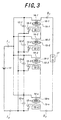
- Fig. 3 is a circuit diagram showing a principal structure of the switching circuit according to the invention.
- a first input terminal I 1 of the switching circuit is connected to a positive terminal of a DC voltage supply source 11 and a second input terminal I 2 is connected to a negative terminal of the voltage supply source 11.
- a plurality of capacitors 12-1, 12-2 ⁇ 12-n are connected in parallel with the DC voltage supply source 11. That is to say, one ends of the capacitors 12-1, 12-2 ⁇ 12-n are commonly connected to the first input terminal I 1 and the other ends of these capacitors are commonly connected to the second input terminal I 2 .
- each of the primary conductors 14-1, 14-2 ⁇ 14-n is magnetically coupled with respective one of the secondary conductors 16-1, 16-2 ⁇ 16-n by means of each of the magnetic cores 15-1, 15-2 ⁇ 15-n.
- a plurality of secondary conductors 16-1, 16-2 ⁇ 16-n are connected in series, and a series arrangement of the secondary conductors is connected across first and second output terminals O 1 and O 2 . These output terminals O 1 and O 2 are connected to a discharge portion 17.
- the semiconductor switching devices 13-1, 13-2 ⁇ 13-n are controlled by driving circuits 18-1, 18-2 ⁇ 18-n, respectively.
- the driving circuits 18-1, 18-2 ⁇ 18-n are operated simultaneously to turn-on the semiconductor switching devices 13-1, 13-2 ⁇ 13-n to discharge charges stored in the capacitors 12-1, 12-2 ⁇ 12-n through the primary conductors 14-1, 14-2 ⁇ 14-n, respectively.
- secondary voltages are induced in the secondary conductors 16-1, 16-2 ⁇ 16-n.
- each of these conductors is wound on each of the magnetic cores 15-1, 15-2 ⁇ 15-n only by one turn.
- the primary and secondary conductors are merely passed through the magnetic cores.
- the switching circuit for generating pulsed power even if all the semiconductor switching devices 13-1, 13-2 ⁇ 13-n are not turned-on simultaneously due to fluctuations in their characteristics, an excessive high voltage is not applied to one or more non-conducting semiconductor switching devices. Furthermore, since the same voltage E is applied to all the semiconductor switching devices 13-1, 13-2 ⁇ 13-n, no high voltage is applied to the driving circuits 18-1, 18-2 ⁇ 18-3. Therefore, it is no more necessary to isolate power supply sources of these driving circuits as well as driving signals from each other. Moreover, it is sufficient to use the DC voltage supply source 11 generating a low output voltage and the capacitors 12-1, 12-2 ⁇ 12-n are not required to be formed to have a high breakdown voltage. In this manner, although the switching circuit according to the invention is somewhat complicated in its construction, respective circuit elements having lower breakdown voltages can be utilized without providing special isolation, and therefore the structure of the switching circuit as a whole becomes very simple and less expensive.
- Fig. 4 is a circuit diagram showing a first embodiment of the switching circuit for generating pulsed power according to the invention.
- a current limiting resistor 22 is connected in series with a DC voltage supply source 21, and this series circuit is connected across the first and second input terminals I 1 and I 2 .
- Ten capacitors 23-1, 23-2 ⁇ 23-10 are connected in parallel with the first and second input terminals I 1 and I 2 .
- the semiconductor switching device is formed by a static induction thyristor.
- One ends of the capacitors 23-1, 23-2 ⁇ 23-10 are connected through primary conductors 24-1, 24-2 ⁇ 24-10 to anodes of static induction thyristors 25-1, 25-2 ⁇ 25-10, respectively, and cathodes of the static induction thyristors are connected to the other ends of the capacitors 23-1, 23-2 ⁇ 23-10, respectively.
- the primary conductors 24-1, 24-2 ⁇ 24-10 are wound on magnetic cores 26-1, 26-2 ⁇ 26-10, respectively by one turn.
- a single insulated conductor 27 constituting a series arrangement of secondary conductors is passed through the magnetic cores 26-1, 26-2 ⁇ 26-10, successively, and both ends of the conductor 27 are connected to the first and second output terminals O 1 and O 2 , respectively connected to a discharge portion 28.
- gate driving circuits 29-1, 29-2 ⁇ 29-10 are connected between the cathodes and the gates of the static induction thyristors 25-1, 25-2 ⁇ 25-10, respectively.
- the switching circuit of the present embodiment operates similarly to that of the principal structure shown in Fig. 3 and its detailed explanation is dispensed with.
- the static induction thyristor has a breakdown voltage of several KV and the DC voltage supply source 21 produces the output voltage of several KV, a high voltage of several tens KV can be applied to the discharge portion 28.
- the DC voltage supply source 21 producing the output voltage of several KV can be constructed by conventional parts in a simple and less expensive manner, and a strict isolation such as the oil insulation is not required.
- the capacitors 23-1, 23-2 ⁇ 23-10 and thyristors 25-1, 25-2 ⁇ 25-10 can be formed to have a breakdown voltage of several KV, and can be small in size and less expensive in cost.
- the isolation of the primary circuit portion from structural members such as chassis can be performed easily without providing special insulating means such as the oil insulation.
- a high voltage is applied to a secondary circuit portion, a plurality of the secondary conductors are formed by the single insulated conductor 27 which can be resist a high voltage and no problem occurs.
- the secondary conductors are formed by the single straight conductor 27, a stray inductance can be minimized and high frequency characteristics can be improved.
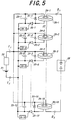
- Fig. 5 is a circuit diagram depicting a second embodiment of the switching circuit for generating pulsed power according to the invention.
- diodes 31-1, 31-2 ⁇ 31-10 are connected in parallel with the primary conductors 24-1, 24-2 ⁇ 24-10, respectively in opposite polarity to the static induction thyristors 25-2, 25-2 ⁇ 25-10. That is to say, the anodes of the diodes 31-1, 31-2 ⁇ 31-10 are connected to the anodes of the thyristors 25-1, 25-2 ⁇ 25-10, respectively.
- a reverse voltage is induced in the primary conductor 24-2 by the current flowing through the secondary conductor 27. If the diode is not provided, the reverse voltage is applied to the thyristor 25-2 and this thyristor might be broken. However, in the present embodiment, the reverse voltage is dissipated by the diode 31-2 and no high voltage is applied to the thyristor 25-2.
- the remaining merits of the switching circuit for generating pulsed power of the present embodiment are same as those of the first embodiment.
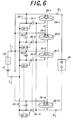
- Fig. 6 is a circuit diagram showing a third embodiment of the switching circuit for generating pulsed power according to the invention.
- portions similar to those of the first and second embodiments shown in Figs. 4 and 5 are denoted by the same reference numerals used in Figs. 4 and 5 and their explanation is dispensed with.
- the anodes of all the static induction thyristors 25-1, 25-2 ⁇ 25-10 are connected to each other. If the thyristor 25-2 is not turned-on, the high reverse voltage induced in the primary conductor 24-2 is dissipated by the remaining turned-on thyristors and the thyristor can be protected against breakdown. Therefore, in the present embodiment, the diodes 31-1, 31-2 ⁇ 31-10 of the second embodiment can be deleted. The remaining merits of the present invention are identical with those of the first embodiment.
- the semiconductor switching device is formed by the static induction thyristor, but according to the invention, it may be constructed by other type thyristors and transistors.
- the semiconductor switching device is formed by the static induction thyristor, but according to the invention, it may be constructed by other type thyristors and transistors.
Landscapes
- Engineering & Computer Science (AREA)
- Power Engineering (AREA)
- Generation Of Surge Voltage And Current (AREA)
- Electronic Switches (AREA)
Abstract
Description
Claims (12)
- A switching circuit for generating pulsed power comprising:first and second input terminals to be connected to a DC voltage supply source;a plurality of capacitors whose one ends are connected commonly to said first input terminal and whose other ends are connected commonly to said second input terminal;a plurality of magnetic cores;a plurality of semiconductor switching devices each of which is connected in parallel with a respective one of the capacitors by means of a respective one of a plurality of primary conductors each being magnetically coupled with a respective one of said plurality of magnetic cores;a plurality of driving circuits for controlling turn-on and turn-off of said plurality of semiconductor switching devices, respectively;a series arrangement of a plurality of secondary conductors each being magnetically coupled with respective magnetic cores; andfirst and second output terminals, both ends of said series arrangement of a plurality of secondary conductors being connected said first and second output terminals, respectively such that a sum of voltages induced in respective secondary conductors is applied across said first and second output terminals.
- The switching circuit according to claim 1, wherein said each of said primary and secondary conductors is passed through each of said magnetic cores once.
- The switching circuit according to claim 2, wherein said series arrangement of secondary conductors is formed by a single conductor passing through said plurality of magnetic cores successively.
- The switching circuit according to claim 1, further comprising a plurality of diodes connected in parallel with respective primary conductors in an opposite polarity to that in which a current flows through the semiconductor switching devices.
- The switching circuit according to claim 1, wherein one ends of the semiconductor switching devices connected to respective primary conductors are connected commonly.
- The switching circuit according to claim 1, wherein each of said semiconductor switching device is formed by a static induction thyristor.
- The switching circuit according to claim 6, wherein said anodes of the static induction thyristors are commonly connected, through the primary conductors, respectively, to said first input terminal to be connected to a positive output terminal of the DC voltage supply source, cathodes of the static induction transistors are commonly connected to said second input terminal to be connected to a negative output terminal of the DC voltage supply source, and said control circuits are formed by gate driving circuits, each of which is connected between an anode and a cathode of a respective one of the static induction thyristors.
- The switching circuit according to claim 7, wherein the anodes of said static induction thyristors are coupled with said first input terminal through parallel circuits of the primary conductors and diodes whose anodes are connected to the anodes of the static induction thyristors.
- The switching circuit according to claim 7, wherein the anodes of said static induction thyristors are commonly connected.
- The switching circuit according to any one of claims 7-9, wherein a current limiting resistor is connected in a circuit for connecting said first and second input terminals to the DC voltage supply source.
- The switching circuit according to any one of claims 7-9, wherein said series arrangement of secondary conductors is formed by a single conductor.
- The switching circuit according to claim 11, wherein said single conductor is straight.
Applications Claiming Priority (2)
| Application Number | Priority Date | Filing Date | Title |
|---|---|---|---|
| JP2000042808A JP2001238470A (en) | 2000-02-21 | 2000-02-21 | Switch circuit for pulse power generation |
| JP2000042808 | 2000-02-21 |
Publications (3)
| Publication Number | Publication Date |
|---|---|
| EP1128557A2 true EP1128557A2 (en) | 2001-08-29 |
| EP1128557A3 EP1128557A3 (en) | 2003-10-29 |
| EP1128557B1 EP1128557B1 (en) | 2008-05-14 |
Family
ID=18565832
Family Applications (1)
| Application Number | Title | Priority Date | Filing Date |
|---|---|---|---|
| EP01301501A Expired - Lifetime EP1128557B1 (en) | 2000-02-21 | 2001-02-20 | Switching circuit for generating pulsed power |
Country Status (5)
| Country | Link |
|---|---|
| US (1) | US6359424B2 (en) |
| EP (1) | EP1128557B1 (en) |
| JP (1) | JP2001238470A (en) |
| KR (1) | KR100399714B1 (en) |
| DE (1) | DE60133958D1 (en) |
Cited By (27)
| Publication number | Priority date | Publication date | Assignee | Title |
|---|---|---|---|---|
| WO2006007274A1 (en) * | 2004-07-01 | 2006-01-19 | Dana Corporation | Semiconductor switch assembly for pulse power apparatus |
| WO2008055546A1 (en) * | 2006-11-09 | 2008-05-15 | Osram Gesellschaft mit beschränkter Haftung | Circuit arrangement |
| CN106105033A (en) * | 2013-11-14 | 2016-11-09 | 鹰港科技有限公司 | high-voltage nanosecond pulse generator |
| EP3167549A4 (en) * | 2014-07-11 | 2018-03-28 | Eagle Harbor Technologies, Inc. | High voltage nanosecond pulser with variable pulse width and pulse repetition frequency |
| US10020800B2 (en) | 2013-11-14 | 2018-07-10 | Eagle Harbor Technologies, Inc. | High voltage nanosecond pulser with variable pulse width and pulse repetition frequency |
| US10304661B2 (en) | 2017-08-25 | 2019-05-28 | Eagle Harbor Technologies, Inc. | Arbitarary waveform generation using nanosecond pulses |
| US10847346B2 (en) | 2014-02-28 | 2020-11-24 | Eagle Harbor Technologies, Inc. | High voltage resistive output stage circuit |
| US10892140B2 (en) | 2018-07-27 | 2021-01-12 | Eagle Harbor Technologies, Inc. | Nanosecond pulser bias compensation |
| US10978955B2 (en) | 2014-02-28 | 2021-04-13 | Eagle Harbor Technologies, Inc. | Nanosecond pulser bias compensation |
| US11171568B2 (en) | 2017-02-07 | 2021-11-09 | Eagle Harbor Technologies, Inc. | Transformer resonant converter |
| US11222767B2 (en) | 2018-07-27 | 2022-01-11 | Eagle Harbor Technologies, Inc. | Nanosecond pulser bias compensation |
| US11227745B2 (en) | 2018-08-10 | 2022-01-18 | Eagle Harbor Technologies, Inc. | Plasma sheath control for RF plasma reactors |
| JP2022519547A (en) * | 2019-01-31 | 2022-03-24 | イーグル ハーバー テクノロジーズ,インク. | Precision plasma control system |
| US11302518B2 (en) | 2018-07-27 | 2022-04-12 | Eagle Harbor Technologies, Inc. | Efficient energy recovery in a nanosecond pulser circuit |
| US11404246B2 (en) | 2019-11-15 | 2022-08-02 | Eagle Harbor Technologies, Inc. | Nanosecond pulser bias compensation with correction |
| US11430635B2 (en) | 2018-07-27 | 2022-08-30 | Eagle Harbor Technologies, Inc. | Precise plasma control system |
| US11527383B2 (en) | 2019-12-24 | 2022-12-13 | Eagle Harbor Technologies, Inc. | Nanosecond pulser RF isolation for plasma systems |
| US11532457B2 (en) | 2018-07-27 | 2022-12-20 | Eagle Harbor Technologies, Inc. | Precise plasma control system |
| US11539352B2 (en) | 2013-11-14 | 2022-12-27 | Eagle Harbor Technologies, Inc. | Transformer resonant converter |
| US11646176B2 (en) | 2019-01-08 | 2023-05-09 | Eagle Harbor Technologies, Inc. | Efficient nanosecond pulser with source and sink capability for plasma control applications |
| US11670484B2 (en) | 2018-11-30 | 2023-06-06 | Eagle Harbor Technologies, Inc. | Variable output impedance RF generator |
| US12230477B2 (en) | 2018-07-27 | 2025-02-18 | Eagle Harbor Technologies, Inc. | Nanosecond pulser ADC system |
| US12348228B2 (en) | 2022-06-29 | 2025-07-01 | EHT Ventures LLC | Bipolar high voltage pulser |
| US12354832B2 (en) | 2022-09-29 | 2025-07-08 | Eagle Harbor Technologies, Inc. | High voltage plasma control |
| US12437967B2 (en) | 2020-07-09 | 2025-10-07 | Eagle Harbor Technologies, Inc. | Ion current droop compensation |
| US12456604B2 (en) | 2019-12-24 | 2025-10-28 | Eagle Harbor Technologies, Inc. | Nanosecond pulser RF isolation for plasma systems |
| US12646683B2 (en) | 2020-05-12 | 2026-06-02 | Eagle Harbor Technologies, Inc. | High frequency RF generator and DC pulsing |
Families Citing this family (24)
| Publication number | Priority date | Publication date | Assignee | Title |
|---|---|---|---|---|
| GB2378065B (en) * | 2001-06-15 | 2004-09-15 | Marconi Applied Technologies | High voltage switching apparatus |
| US6741484B2 (en) * | 2002-01-04 | 2004-05-25 | Scandinova Ab | Power modulator having at least one pulse generating module; multiple cores; and primary windings parallel-connected such that each pulse generating module drives all cores |
| KR100430670B1 (en) * | 2002-05-02 | 2004-05-10 | 한국전기연구원 | Circuit for generating voltage pulse having serial arrangement of boost type converter |
| EP1363386B1 (en) | 2002-05-13 | 2005-01-05 | Luxon Energy Devices Corporation | High current pulse generator |
| EP2395226B1 (en) * | 2003-07-28 | 2013-07-17 | Phillips and Temro Industries Inc. | Controller for air intake heater |
| US7095179B2 (en) * | 2004-02-22 | 2006-08-22 | Zond, Inc. | Methods and apparatus for generating strongly-ionized plasmas with ionizational instabilities |
| US20060066248A1 (en) * | 2004-09-24 | 2006-03-30 | Zond, Inc. | Apparatus for generating high current electrical discharges |
| US7663319B2 (en) * | 2004-02-22 | 2010-02-16 | Zond, Inc. | Methods and apparatus for generating strongly-ionized plasmas with ionizational instabilities |
| US9123508B2 (en) * | 2004-02-22 | 2015-09-01 | Zond, Llc | Apparatus and method for sputtering hard coatings |
| RU2269850C1 (en) * | 2004-08-10 | 2006-02-10 | Институт мониторинга климатических и экологических систем | Scheme of excitation of lasers on metal fume |
| GB0503439D0 (en) * | 2005-02-18 | 2005-03-30 | E2V Tech Uk Ltd | High voltage switching apparatus |
| JP2006324039A (en) * | 2005-05-17 | 2006-11-30 | Ushio Inc | Pulse generator and extreme ultraviolet light source device |
| US7633182B2 (en) * | 2005-11-09 | 2009-12-15 | Bae Systems Advanced Technologies, Inc. | Bipolar pulse generators with voltage multiplication |
| US8036008B2 (en) * | 2006-09-15 | 2011-10-11 | Mitsubishi Electric Corporation | DC/DC power converting apparatus |
| US8133359B2 (en) | 2007-11-16 | 2012-03-13 | Advanced Energy Industries, Inc. | Methods and apparatus for sputtering deposition using direct current |
| US9039871B2 (en) | 2007-11-16 | 2015-05-26 | Advanced Energy Industries, Inc. | Methods and apparatus for applying periodic voltage using direct current |
| JP2009184862A (en) * | 2008-02-05 | 2009-08-20 | Ngk Insulators Ltd | Plasma reactor |
| US7903434B2 (en) * | 2008-06-23 | 2011-03-08 | Scandinova Systems Ab | Power switch grouping |
| DE102013207329A1 (en) * | 2013-04-23 | 2014-10-23 | Siemens Aktiengesellschaft | Inductive isolation of voltage sources of an IVA by means of single coupled coils |
| CA2818450C (en) | 2013-06-17 | 2020-04-07 | Enedym Inc. | Reconfigurable hybrid energy storage system for electrified vehicles |
| US10268846B2 (en) * | 2016-12-30 | 2019-04-23 | Eagle Harbor Technologies, Inc. | High voltage inductive adder |
| US11452870B2 (en) * | 2019-12-18 | 2022-09-27 | Pulse Biosciences, Inc. | Nanosecond pulsed power sources having multi-core transformers |
| WO2021255875A1 (en) | 2020-06-17 | 2021-12-23 | 三菱電機株式会社 | Pulse power supply device |
| CN114675625B (en) * | 2022-03-21 | 2024-11-19 | 潍柴动力股份有限公司 | Controller control method and device |
Family Cites Families (5)
| Publication number | Priority date | Publication date | Assignee | Title |
|---|---|---|---|---|
| FR2544579B1 (en) * | 1983-04-15 | 1986-05-16 | Cgr Mev | POWER MODULATOR PROVIDED WITH A TRANSFORMER |
| US5365421A (en) * | 1992-12-14 | 1994-11-15 | Texas Instruments Incorporated | Pulse transformer having plural simultaneously operable primary windings and a single secondary winding |
| SE9604814D0 (en) * | 1996-12-20 | 1996-12-20 | Scanditronix Medical Ab | Power modulator |
| US5914974A (en) * | 1997-02-21 | 1999-06-22 | Cymer, Inc. | Method and apparatus for eliminating reflected energy due to stage mismatch in nonlinear magnetic compression modules |
| US6055161A (en) * | 1999-04-12 | 2000-04-25 | Lincoln Global, Inc. | Switching type power supply for arc welding |
-
2000
- 2000-02-21 JP JP2000042808A patent/JP2001238470A/en active Pending
-
2001
- 2001-02-16 US US09/788,312 patent/US6359424B2/en not_active Expired - Fee Related
- 2001-02-20 DE DE60133958T patent/DE60133958D1/en not_active Expired - Lifetime
- 2001-02-20 EP EP01301501A patent/EP1128557B1/en not_active Expired - Lifetime
- 2001-02-20 KR KR10-2001-0008378A patent/KR100399714B1/en not_active Expired - Fee Related
Cited By (54)
| Publication number | Priority date | Publication date | Assignee | Title |
|---|---|---|---|---|
| WO2006007274A1 (en) * | 2004-07-01 | 2006-01-19 | Dana Corporation | Semiconductor switch assembly for pulse power apparatus |
| GB2430566A (en) * | 2004-07-01 | 2007-03-28 | Dana Corp | Semiconductor switch assembly for pulse power apparatus |
| GB2430566B (en) * | 2004-07-01 | 2008-06-04 | Dana Corp | Semiconductor switch assembly for pulse power apparatus |
| US7514819B2 (en) | 2004-07-01 | 2009-04-07 | Dana Automotive Systems Group, Llc | Semiconductor switch assembly for pulse power apparatus |
| WO2008055546A1 (en) * | 2006-11-09 | 2008-05-15 | Osram Gesellschaft mit beschränkter Haftung | Circuit arrangement |
| KR101369797B1 (en) * | 2006-11-09 | 2014-03-06 | 오스람 게엠베하 | Circuit arrangement |
| US10985740B2 (en) | 2013-11-14 | 2021-04-20 | Eagle Harbor Technologies, Inc. | High voltage nanosecond pulser with variable pulse width and pulse repetition frequency |
| EP3069445A4 (en) * | 2013-11-14 | 2017-12-06 | Eagle Harbor Technologies, Inc. | High voltage nanosecond pulser |
| US11539352B2 (en) | 2013-11-14 | 2022-12-27 | Eagle Harbor Technologies, Inc. | Transformer resonant converter |
| US9960763B2 (en) | 2013-11-14 | 2018-05-01 | Eagle Harbor Technologies, Inc. | High voltage nanosecond pulser |
| US10020800B2 (en) | 2013-11-14 | 2018-07-10 | Eagle Harbor Technologies, Inc. | High voltage nanosecond pulser with variable pulse width and pulse repetition frequency |
| CN106105033B (en) * | 2013-11-14 | 2019-04-12 | 鹰港科技有限公司 | High-voltage nanosecond pulse generator |
| US11558048B2 (en) | 2013-11-14 | 2023-01-17 | Eagle Harbor Technologies, Inc. | High voltage nanosecond pulser |
| US10382022B2 (en) | 2013-11-14 | 2019-08-13 | Eagle Harbor Technologies, Inc. | High voltage nanosecond pulser with variable pulse width and pulse repetition frequency |
| CN106105033A (en) * | 2013-11-14 | 2016-11-09 | 鹰港科技有限公司 | high-voltage nanosecond pulse generator |
| US10707864B2 (en) | 2013-11-14 | 2020-07-07 | Eagle Harbor Technologies, Inc. | High voltage nanosecond pulser |
| US11159156B2 (en) | 2013-11-14 | 2021-10-26 | Eagle Harbor Technologies, Inc. | High voltage nanosecond pulser |
| EP4210223A1 (en) * | 2013-11-14 | 2023-07-12 | Eagle Harbor Technologies, Inc. | High voltage nanosecond pulser |
| US11502672B2 (en) | 2013-11-14 | 2022-11-15 | Eagle Harbor Technologies, Inc. | High voltage nanosecond pulser with variable pulse width and pulse repetition frequency |
| US12451811B2 (en) | 2014-02-28 | 2025-10-21 | EHT Ventures LLC | Nanosecond pulser bias compensation |
| US10978955B2 (en) | 2014-02-28 | 2021-04-13 | Eagle Harbor Technologies, Inc. | Nanosecond pulser bias compensation |
| US10847346B2 (en) | 2014-02-28 | 2020-11-24 | Eagle Harbor Technologies, Inc. | High voltage resistive output stage circuit |
| US11689107B2 (en) | 2014-02-28 | 2023-06-27 | Eagle Harbor Technologies, Inc. | Nanosecond pulser bias compensation |
| US11631573B2 (en) | 2014-02-28 | 2023-04-18 | Eagle Harbor Technologies, Inc. | High voltage resistive output stage circuit |
| EP3528386A1 (en) * | 2014-07-11 | 2019-08-21 | Eagle Harbor Technologies, Inc. | High voltage nanosecond pulser with variable pulse width and pulse repetition frequency |
| EP3167549A4 (en) * | 2014-07-11 | 2018-03-28 | Eagle Harbor Technologies, Inc. | High voltage nanosecond pulser with variable pulse width and pulse repetition frequency |
| US11171568B2 (en) | 2017-02-07 | 2021-11-09 | Eagle Harbor Technologies, Inc. | Transformer resonant converter |
| US12555745B2 (en) | 2017-08-25 | 2026-02-17 | Eagle Harbor Technologies, Inc. | Apparatus and method of generating a waveform |
| US10777388B2 (en) | 2017-08-25 | 2020-09-15 | Eagle Harbor Technologies, Inc. | Arbitrary waveform generation using digital pulses |
| US10304661B2 (en) | 2017-08-25 | 2019-05-28 | Eagle Harbor Technologies, Inc. | Arbitarary waveform generation using nanosecond pulses |
| US11387076B2 (en) | 2017-08-25 | 2022-07-12 | Eagle Harbor Technologies, Inc. | Apparatus and method of generating a waveform |
| US11222767B2 (en) | 2018-07-27 | 2022-01-11 | Eagle Harbor Technologies, Inc. | Nanosecond pulser bias compensation |
| US11587768B2 (en) | 2018-07-27 | 2023-02-21 | Eagle Harbor Technologies, Inc. | Nanosecond pulser thermal management |
| US10892140B2 (en) | 2018-07-27 | 2021-01-12 | Eagle Harbor Technologies, Inc. | Nanosecond pulser bias compensation |
| US10892141B2 (en) | 2018-07-27 | 2021-01-12 | Eagle Harbor Technologies, Inc. | Nanosecond pulser pulse generation |
| US11532457B2 (en) | 2018-07-27 | 2022-12-20 | Eagle Harbor Technologies, Inc. | Precise plasma control system |
| US11302518B2 (en) | 2018-07-27 | 2022-04-12 | Eagle Harbor Technologies, Inc. | Efficient energy recovery in a nanosecond pulser circuit |
| US11430635B2 (en) | 2018-07-27 | 2022-08-30 | Eagle Harbor Technologies, Inc. | Precise plasma control system |
| US12230477B2 (en) | 2018-07-27 | 2025-02-18 | Eagle Harbor Technologies, Inc. | Nanosecond pulser ADC system |
| US11875971B2 (en) | 2018-07-27 | 2024-01-16 | Eagle Harbor Technologies, Inc. | Efficient energy recovery in a nanosecond pulser circuit |
| US10991553B2 (en) | 2018-07-27 | 2021-04-27 | Eagle Harbor Technologies, Inc. | Nanosecond pulser thermal management |
| US11101108B2 (en) | 2018-07-27 | 2021-08-24 | Eagle Harbor Technologies Inc. | Nanosecond pulser ADC system |
| US11227745B2 (en) | 2018-08-10 | 2022-01-18 | Eagle Harbor Technologies, Inc. | Plasma sheath control for RF plasma reactors |
| US11670484B2 (en) | 2018-11-30 | 2023-06-06 | Eagle Harbor Technologies, Inc. | Variable output impedance RF generator |
| US12198898B2 (en) | 2018-11-30 | 2025-01-14 | Eagle Harbor Technologies, Inc. | Variable output impedance RF generator |
| US11646176B2 (en) | 2019-01-08 | 2023-05-09 | Eagle Harbor Technologies, Inc. | Efficient nanosecond pulser with source and sink capability for plasma control applications |
| JP2022519547A (en) * | 2019-01-31 | 2022-03-24 | イーグル ハーバー テクノロジーズ,インク. | Precision plasma control system |
| US11404246B2 (en) | 2019-11-15 | 2022-08-02 | Eagle Harbor Technologies, Inc. | Nanosecond pulser bias compensation with correction |
| US11527383B2 (en) | 2019-12-24 | 2022-12-13 | Eagle Harbor Technologies, Inc. | Nanosecond pulser RF isolation for plasma systems |
| US12456604B2 (en) | 2019-12-24 | 2025-10-28 | Eagle Harbor Technologies, Inc. | Nanosecond pulser RF isolation for plasma systems |
| US12646683B2 (en) | 2020-05-12 | 2026-06-02 | Eagle Harbor Technologies, Inc. | High frequency RF generator and DC pulsing |
| US12437967B2 (en) | 2020-07-09 | 2025-10-07 | Eagle Harbor Technologies, Inc. | Ion current droop compensation |
| US12348228B2 (en) | 2022-06-29 | 2025-07-01 | EHT Ventures LLC | Bipolar high voltage pulser |
| US12354832B2 (en) | 2022-09-29 | 2025-07-08 | Eagle Harbor Technologies, Inc. | High voltage plasma control |
Also Published As
| Publication number | Publication date |
|---|---|
| JP2001238470A (en) | 2001-08-31 |
| US20010030527A1 (en) | 2001-10-18 |
| EP1128557B1 (en) | 2008-05-14 |
| DE60133958D1 (en) | 2008-06-26 |
| KR100399714B1 (en) | 2003-09-29 |
| US6359424B2 (en) | 2002-03-19 |
| KR20010083187A (en) | 2001-08-31 |
| EP1128557A3 (en) | 2003-10-29 |
Similar Documents
| Publication | Publication Date | Title |
|---|---|---|
| EP1128557B1 (en) | Switching circuit for generating pulsed power | |
| US6788012B2 (en) | Circuit for generating high voltage pulse | |
| US11456155B2 (en) | High voltage switch with isolated power | |
| US11875971B2 (en) | Efficient energy recovery in a nanosecond pulser circuit | |
| EP3830859B1 (en) | High voltage power system with bias compensation | |
| KR20240028538A (en) | Efficient energy recovery in a nanosecond pulser circuit | |
| US10460911B2 (en) | High voltage resistive output stage circuit | |
| RU2298871C2 (en) | High-power modulator | |
| EP0434048A2 (en) | Compact high voltage power supply | |
| US7072196B1 (en) | Multi-stage high voltage solid state switch | |
| Mortazavi et al. | Ultrafast Switching of Series-Connected MOSFETs for High-Voltage Nanosecond Pulsed Applications | |
| Casey et al. | Solid-state Marx bank modulator for the next linear collider | |
| Korzhenevskiy et al. | Output voltage adjustment of a pulsed high-voltage nanosecond generator with inductive energy storage and a solid-state switching system | |
| Cassel et al. | A new type high voltage fast rise/fall time solid state Marx pulse modulator | |
| KR100581490B1 (en) | Drive system of high pressure switching system | |
| RU2408135C1 (en) | Pulse solid modulator | |
| Glidden et al. | Solid state Marx generator | |
| Kuthi et al. | Marx generator using pseudospark switches | |
| Munir et al. | Design of a novel gate driver circuit for a Marx generator based 40kV electric fence energizer | |
| JP3246858B2 (en) | Power supply | |
| Ghasemi et al. | Fast high-voltage, high-current switching using stacked IGBTs | |
| JPH0316414A (en) | Pulse generating circuit | |
| JP2000209876A (en) | Pulse power supply | |
| Strowitzki | Bridge topology as primary switch for magnetic pulse compression circuit | |
| Kawabata et al. | Development of the high voltage power switching circuit with GTOs operated by new gate-drive system |
Legal Events
| Date | Code | Title | Description |
|---|---|---|---|
| PUAI | Public reference made under article 153(3) epc to a published international application that has entered the european phase |
Free format text: ORIGINAL CODE: 0009012 |
|
| AK | Designated contracting states |
Kind code of ref document: A2 Designated state(s): AT BE CH CY DE DK ES FI FR GB GR IE IT LI LU MC NL PT SE TR |
|
| AX | Request for extension of the european patent |
Free format text: AL;LT;LV;MK;RO;SI |
|
| PUAL | Search report despatched |
Free format text: ORIGINAL CODE: 0009013 |
|
| AK | Designated contracting states |
Kind code of ref document: A3 Designated state(s): AT BE CH CY DE DK ES FI FR GB GR IE IT LI LU MC NL PT SE TR |
|
| AX | Request for extension of the european patent |
Extension state: AL LT LV MK RO SI |
|
| AKX | Designation fees paid |
Designated state(s): CH DE FR GB LI |
|
| 17P | Request for examination filed |
Effective date: 20040427 |
|
| GRAP | Despatch of communication of intention to grant a patent |
Free format text: ORIGINAL CODE: EPIDOSNIGR1 |
|
| GRAS | Grant fee paid |
Free format text: ORIGINAL CODE: EPIDOSNIGR3 |
|
| GRAA | (expected) grant |
Free format text: ORIGINAL CODE: 0009210 |
|
| AK | Designated contracting states |
Kind code of ref document: B1 Designated state(s): CH DE FR GB LI |
|
| REG | Reference to a national code |
Ref country code: GB Ref legal event code: FG4D |
|
| REG | Reference to a national code |
Ref country code: CH Ref legal event code: EP |
|
| REF | Corresponds to: |
Ref document number: 60133958 Country of ref document: DE Date of ref document: 20080626 Kind code of ref document: P |
|
| PLBE | No opposition filed within time limit |
Free format text: ORIGINAL CODE: 0009261 |
|
| STAA | Information on the status of an ep patent application or granted ep patent |
Free format text: STATUS: NO OPPOSITION FILED WITHIN TIME LIMIT |
|
| 26N | No opposition filed |
Effective date: 20090217 |
|
| PGFP | Annual fee paid to national office [announced via postgrant information from national office to epo] |
Ref country code: CH Payment date: 20120126 Year of fee payment: 12 Ref country code: FR Payment date: 20120203 Year of fee payment: 12 |
|
| PGFP | Annual fee paid to national office [announced via postgrant information from national office to epo] |
Ref country code: DE Payment date: 20120229 Year of fee payment: 12 |
|
| PGFP | Annual fee paid to national office [announced via postgrant information from national office to epo] |
Ref country code: GB Payment date: 20120127 Year of fee payment: 12 |
|
| REG | Reference to a national code |
Ref country code: CH Ref legal event code: PL |
|
| GBPC | Gb: european patent ceased through non-payment of renewal fee |
Effective date: 20130220 |
|
| PG25 | Lapsed in a contracting state [announced via postgrant information from national office to epo] |
Ref country code: LI Free format text: LAPSE BECAUSE OF NON-PAYMENT OF DUE FEES Effective date: 20130228 Ref country code: CH Free format text: LAPSE BECAUSE OF NON-PAYMENT OF DUE FEES Effective date: 20130228 |
|
| REG | Reference to a national code |
Ref country code: FR Ref legal event code: ST Effective date: 20131031 |
|
| REG | Reference to a national code |
Ref country code: DE Ref legal event code: R119 Ref document number: 60133958 Country of ref document: DE Effective date: 20130903 |
|
| PG25 | Lapsed in a contracting state [announced via postgrant information from national office to epo] |
Ref country code: FR Free format text: LAPSE BECAUSE OF NON-PAYMENT OF DUE FEES Effective date: 20130228 Ref country code: DE Free format text: LAPSE BECAUSE OF NON-PAYMENT OF DUE FEES Effective date: 20130903 Ref country code: GB Free format text: LAPSE BECAUSE OF NON-PAYMENT OF DUE FEES Effective date: 20130220 |