EP1128554A2 - Active inductor - Google Patents
Active inductor Download PDFInfo
- Publication number
- EP1128554A2 EP1128554A2 EP01301553A EP01301553A EP1128554A2 EP 1128554 A2 EP1128554 A2 EP 1128554A2 EP 01301553 A EP01301553 A EP 01301553A EP 01301553 A EP01301553 A EP 01301553A EP 1128554 A2 EP1128554 A2 EP 1128554A2
- Authority
- EP
- European Patent Office
- Prior art keywords
- mosfet
- active inductor
- gate
- drain
- source
- Prior art date
- Legal status (The legal status is an assumption and is not a legal conclusion. Google has not performed a legal analysis and makes no representation as to the accuracy of the status listed.)
- Withdrawn
Links
- 239000003990 capacitor Substances 0.000 claims abstract description 30
- 238000010586 diagram Methods 0.000 description 13
- 238000000034 method Methods 0.000 description 6
- 230000003071 parasitic effect Effects 0.000 description 6
- 230000015572 biosynthetic process Effects 0.000 description 2
- 238000002955 isolation Methods 0.000 description 2
- 230000004048 modification Effects 0.000 description 2
- 238000012986 modification Methods 0.000 description 2
- 239000000758 substrate Substances 0.000 description 2
- 239000000470 constituent Substances 0.000 description 1
- 230000001419 dependent effect Effects 0.000 description 1
- 230000000694 effects Effects 0.000 description 1
- 230000005669 field effect Effects 0.000 description 1
- 239000012212 insulator Substances 0.000 description 1
- 230000010354 integration Effects 0.000 description 1
- 239000002184 metal Substances 0.000 description 1
- 229910021420 polycrystalline silicon Inorganic materials 0.000 description 1
- 229920005591 polysilicon Polymers 0.000 description 1
- 239000004065 semiconductor Substances 0.000 description 1
- 238000005549 size reduction Methods 0.000 description 1
- 230000001629 suppression Effects 0.000 description 1
Images


Classifications
-
- H—ELECTRICITY
- H03—ELECTRONIC CIRCUITRY
- H03H—IMPEDANCE NETWORKS, e.g. RESONANT CIRCUITS; RESONATORS
- H03H11/00—Networks using active elements
- H03H11/46—One-port networks
- H03H11/48—One-port networks simulating reactances
-
- H—ELECTRICITY
- H10—SEMICONDUCTOR DEVICES; ELECTRIC SOLID-STATE DEVICES NOT OTHERWISE PROVIDED FOR
- H10D—INORGANIC ELECTRIC SEMICONDUCTOR DEVICES
- H10D84/00—Integrated devices formed in or on semiconductor substrates that comprise only semiconducting layers, e.g. on Si wafers or on GaAs-on-Si wafers
Definitions
- the present invention relates to an active inductor and, more particularly, to an active inductor with its inductance electrically controllable, which comprises an MOSFET and a single capacitor for applications to RF (radio frequency) integrated circuits, high frequency VCOs and the like.
- inductors are implemented as passive elements employing metal spirals or bonding wires for use in filters, oscillators, RF tuned circuits and the like.
- An active inductor with its inductance electrically controllable is disclosed in Japanese Unexamined Patent Publication No. Sho 63(1988)-219150 (Reference 1).
- the active inductor employs two cascade-connected FETs (field effect transistors) and a feedback resistor for suppression of a reduction in the inductance thereof and for size reduction thereof.
- This active inductor is also disclosed in IEEE Transactions on Microwave Theory and Techniques, Vol. 37, No. 12 (Dec. 1989), pp. 1979-1984.
- the active inductor (not shown) disclosed in Reference 1 has an output inductance Zo expressed as follows: Zo ⁇ (1+j ⁇ Cgs ⁇ R)/gm wherein Cgs is the gate-source capacitance of the FETs, gm is the transconductance of the FETs, R is a feedback resistance, and ⁇ is a resonant frequency.
- the gate-source capacitance Cgs of the FETs serves to provide the inductance.
- An active inductor disclosed in Japanese Unexamined Patent Publication No. Hei 2(1990)-205107 is a modification of the active inductor of Reference 1, which employs an FET instead of the feedback resistor R.
- An active inductor disclosed in Japanese Unexamined Patent Publication No. Hei 8(1996)-181571 (Reference 3) comprises three FETs and four capacitors C. The capacitors are used for DC isolation of the transistors.
- An active inductor disclosed in Japanese Unexamined Patent Publication No. Hei 8(1996)-274584 (Reference 4) comprises a source-grounded FET, two cascade-connected FETs, three capacitors C and a resistor R.
- Fig. 7(a) is a diagram illustrating a high frequency equivalent circuit of the active inductor
- Fig. 7(b) is a diagram illustrating an output impedance characteristic with respect to the frequency of the active inductor.
- Cp Cgs ⁇ ( ⁇ Cgs/gm) 2 +Cm wherein Cm is a layout-dependent parasitic capacitance. The parasitic capacitance should be minimized to extend the frequency range of the inductor.
- the active inductors having the circuit configurations of References 1 and 2 are problematic in that the inductance thereof is determined by the gate-source capacitance Cgs of the FETs.
- the active inductors having the circuit configurations of References 3 and 4 are problematic in that the capacitors C should be additionally employed for DC isolation of the FETs. This results in complication and size increase of the circuits constituting the active inductors.
- the present invention is directed to an active inductor which comprises an MOSFET and a single capacitor and features a reduced size and an excellent frequency response characteristic as compared with the conventional active inductors.
- the active inductor can have an excellent frequency response characteristic and a reduced size as compared with the conventional active inductors.
- the active inductor can have an excellent frequency response characteristic and a reduced size as compared with the conventional active inductors.
- the inductance Leq may electrically be varied by adjusting the transconductance gm of the voltage-controlled constant current source.
- the inductance Leq may electrically be varied by adjusting the transconductance gm1 of the MOSFET.
- the voltage-controlled constant current source may comprise an NMOSFET and a PMOSFET cascade-connected to each other, and each having a gate, a drain and a source, the drain of the NMOSFET being kept at a fixed potential, the gate of the NMOSFET being connected to the drain of the MOSFET, the source of the NMOSFET being connected to the source of the PMOSFET, the gate of the PMOSFET being connected to a variable potential, the drain of the PMOSFET being connected to the gate of the MOSFET.
- the voltage-controlled constant current source may comprise a PMOSFET having a source connected to the drain of the MOSFET, a gate connected to a variable potential, and a drain connected to the gate of the MOSFET.
- the present invention further provides an active inductor, which comprises two NMOSFETs each having a gate, a drain serving as an output terminal and a grounded source; two PMOSFETs each having a gate, a drain and a source, the gates thereof being connected together to a DC potential, the sources thereof being respectively connected to the drains of the NMOSFETs; and a single capacitor having opposite ends respectively connected to the gates of the NMOSFETs.
- an active inductor which comprises two NMOSFETs each having a gate, a drain serving as an output terminal and a grounded source; two PMOSFETs each having a gate, a drain and a source, the gates thereof being connected together to a DC potential, the sources thereof being respectively connected to the drains of the NMOSFETs; and a single capacitor having opposite ends respectively connected to the gates of the NMOSFETs.
- the active inductor has an inductance which may electrically be varied by adjusting the transconductance of the two PMOSFETs.
- the active inductor has an inductance which may electrically be varied by adjusting a DC voltage to be applied to the gates of the two PMOSFETs.
- Fig. 1 is a diagram illustrating a basic circuit configuration to be employed in an active inductor according to the present invention.
- the electric current Io is supplied to the capacitor C from the voltage-controlled constant current source, and determines the gate voltage V of the MOSFET.
- Fig. 2 is a diagram illustrating the circuit configuration of an active inductor according to Example 1 of the invention.
- This active inductor comprises three transistors including an MOSFET M1, a PMOSFET M2, and an NMOSFET M3, and a single capacitor C biased in saturation.
- a parasitic capacitance which limits the maximum operating range of this circuit is affected by the capacitance at an output node.
- a major contributor to the parasitic capacitance is the gate capacitance of the NMOSFET M3 for applications to high frequency (RF) circuits.
- Fig. 3 is a diagram illustrating the circuit configuration of an active inductor according to Example 2 of the invention.
- This active inductor comprises two transistors including an MOSFET M1 and a PMOSFET M2, and a single capacitor.
- the output capacitance is determined by the source capacitance of the PMOSFET M2, which is much smaller than the gate capacitance of the NMOSFET M3 shown in Fig. 2.
- Fig. 4 is a diagram illustrating the circuit configuration of an active inductor according to Example 3 of the invention.
- This active inductor comprises four transistors including MOSFETs M1, M3 and PMOSFETs M2, M4, and a single capacitor. That is, a pair of circuits as shown in Fig. 3 are combined together to constitute a differential active inductor with a floating capacitor C.
- This differential active inductor has an inductance which is electrically controllable by changing the transconductance of the MOSFET.
- the active inductors according to the present invention can be implemented in any semiconductor integrated processes.
- the maximum operating frequency of any of these circuits of the active inductors is limited by the maximum operating frequency of the MOSFETs and parasitic capacitances. Therefore, a CMOS process with high frequency transistors (cut-off frequency ft: 20GHz) is required for applications to high frequency circuits (e.g., RF to 2GHz). Formation of a CMOS on an SOI (silicon-on-insulator) substrate is very advantageous in that source-drain junction capacitances are reduced.
- Fig. 5 is a diagram illustrating the circuit configuration of an active inductor according to Example 4 of the invention.
- the circuit configuration shown in Fig. 5 is a modification of the circuit configuration of Fig. 2, and includes a DC bias circuit.
- This active inductor comprises 13 transistors including NMOSFETs M1, M2, M4, M5, M6, M6, M8, M10, M11 and PMOSFETs M3, M7, M9, M12, M13, and a single capacitor.
- the NMOSFETs M1, M2 and the PMOSFET M3 are core transistors (corresponding to the three MOSFETs shown in Fig. 2) which determine the inductance.
- the NMOSFET M10 is cascade-connected in series to the NMOSFET M1 to increase its output resistance ro.
- the NMOSFET M4 is used to set the DC bias point of the NMOSFET M2 and the PMOSFET M3.
- the PMOSFETs M12, M13 constitute a current mirror circuit to set the bias current via the NMOSFET M5 for the NMOSFETs M4, M6, and via the PMOSFET M9 for the NMOSFET M1. It is noted that Io is an external bias current.
- the drain-source resistance rds 4 of the NMOSFET M4 limits the output impedance.
- the output resistance ro of this circuit is given by the following expression: ro ⁇ 1/(gm1 ⁇ gm 2,3 ⁇ rds 4 ) wherein gm 2,3 is the transconductance of the NMOSFET M2 and the PMOSFET M3 in combination.
- the output node of the circuit is denoted by Vo.
- the circuit configuration shown in Fig. 5 is merely an example which may be employed for relatively low frequency applications, and all the bias transistor network is of course included for integration in a CMOS process.
- the bias circuit can also be implemented with the use of passive components (e.g., resistors).
- Fig. 6 is a graph illustrating an output impedance characteristic of the active inductor of Example 4 with respect to the frequency.
- the output impedance Zo (measured value) at the node Vo is shown as a function of the frequency.
- the output impedance Zo of the circuit is approximately 25 ⁇ .
- the inductance is determined by the transconductance of the transistors, the bias current and the capacitance of the capacitor C.
- the formation of the capacitor C can be achieved by utilizing a double-polysilicon capacitor process.
- the frequency response and the inductance are adjusted by changing the bias current Io.
- the active inductors according to the present invention are each implemented by employing a circuit configuration including at least one MOSFET and a single capacitor C. As compared with the conventional circuit configurations and the conventional passive components for the inductors, the following effects are noted.
- the active inductors according to the present invention each have an excellent frequency response characteristic and a reduced size as compared with the conventional active inductors.
Landscapes
- Networks Using Active Elements (AREA)
Abstract
Description
- This application is related to Japanese patent application No. 2000-042949 filed on February 21, 2000, whose priority is claimed under 35 USC §119, the disclosure of which is incorporated by reference in its entirety.
- The present invention relates to an active inductor and, more particularly, to an active inductor with its inductance electrically controllable, which comprises an MOSFET and a single capacitor for applications to RF (radio frequency) integrated circuits, high frequency VCOs and the like.
- In general, inductors are implemented as passive elements employing metal spirals or bonding wires for use in filters, oscillators, RF tuned circuits and the like.
- An active inductor with its inductance electrically controllable is disclosed in Japanese Unexamined Patent Publication No. Sho 63(1988)-219150 (Reference 1). The active inductor employs two cascade-connected FETs (field effect transistors) and a feedback resistor for suppression of a reduction in the inductance thereof and for size reduction thereof. This active inductor is also disclosed in IEEE Transactions on Microwave Theory and Techniques, Vol. 37, No. 12 (Dec. 1989), pp. 1979-1984.
- The active inductor (not shown) disclosed in Reference 1 has an output inductance Zo expressed as follows:
- An active inductor disclosed in Japanese Unexamined Patent Publication No. Hei 2(1990)-205107 (Reference 2) is a modification of the active inductor of Reference 1, which employs an FET instead of the feedback resistor R. In this case, the feedback resistance R is expressed as R=1/gmf, wherein gmf is the transconductance of the feedback transistor.
- An active inductor disclosed in Japanese Unexamined Patent Publication No. Hei 8(1996)-181571 (Reference 3) comprises three FETs and four capacitors C. The capacitors are used for DC isolation of the transistors.
- An active inductor disclosed in Japanese Unexamined Patent Publication No. Hei 8(1996)-274584 (Reference 4) comprises a source-grounded FET, two cascade-connected FETs, three capacitors C and a resistor R.
- In general, the high frequency operation range of an active inductor is limited by stray capacitances that resonate with an equivalent inductor.
- Fig. 7(a) is a diagram illustrating a high frequency equivalent circuit of the active inductor, and Fig. 7(b) is a diagram illustrating an output impedance characteristic with respect to the frequency of the active inductor.
- As shown in Fig. 7(b), a peak Zo in the output impedance characteristic is observed at a resonance frequency ωo, which is given by the following expression:
- The active inductors having the circuit configurations of References 1 and 2 are problematic in that the inductance thereof is determined by the gate-source capacitance Cgs of the FETs.
- The active inductors having the circuit configurations of References 3 and 4 are problematic in that the capacitors C should be additionally employed for DC isolation of the FETs. This results in complication and size increase of the circuits constituting the active inductors.
- In view of the foregoing, the present invention is directed to an active inductor which comprises an MOSFET and a single capacitor and features a reduced size and an excellent frequency response characteristic as compared with the conventional active inductors.
- In accordance with the present invention, there is provided an active inductor comprising: an MOSFET having a gate, a drain serving as an output terminal and a grounded source, the MOSFET having a transconductance gm1; and a capacitor having opposite ends, one of which is grounded and the other of which is connected to the gate of the MOSFET and to a voltage-controlled constant current source having a transconductance gm, the capacitor having a capacitance C; the active inductor being operative with a small-signal output impedance Zo between the output terminal and the ground expressed as Zo=jω{C/(gm1·gm)} (wherein ω is an angular frequency) and with an inductance Leq expressed as Leq={C/(gm1·gm)}.
- With this arrangement, the active inductor can have an excellent frequency response characteristic and a reduced size as compared with the conventional active inductors.
-
- Fig. 1 is a diagram illustrating a basic circuit configuration to be employed in an active inductor according to the present invention;
- Fig. 2 is a diagram illustrating the circuit configuration of an active inductor according to Example 1 of the invention;
- Fig. 3 is a diagram illustrating the circuit configuration of an active inductor according to Example 2 of the invention;
- Fig. 4 is a diagram illustrating the circuit configuration of an active inductor according to Example 3 of the invention;
- Fig. 5 is a diagram illustrating the circuit configuration of an active inductor according to Example 4 of the invention;
- Fig. 6 is a graph illustrating an output impedance characteristic of the active inductor of Example 4 with respect to the frequency;
- Fig. 7(a) is a diagram illustrating a high-frequency equivalent circuit of a conventional active inductor, and Fig. 7(b) is a graph illustrating an output impedance characteristic of the conventional active inductor.
-
- An active inductor according to the present invention comprises an MOSFET having a gate, a drain serving as an output terminal and a grounded source, the MOSFET having a transconductance gml; and a capacitor having opposite ends, one of which is grounded and the other of which is connected to the gate of the MOSFET and to a voltage-controlled constant current source having a transconductance gm, the capacitor having a capacitance C; the active inductor being operative with a small-signal output impedance Zo between the output terminal and the ground expressed as Zo=jω {C/(gm1·gm)} (wherein ω is an angular frequency) and with an inductance Leq expressed as Leq={C/(gm1·gm)}.
- With this arrangement, the active inductor can have an excellent frequency response characteristic and a reduced size as compared with the conventional active inductors.
- The inductance Leq may electrically be varied by adjusting the transconductance gm of the voltage-controlled constant current source.
- The inductance Leq may electrically be varied by adjusting the transconductance gm1 of the MOSFET.
- The voltage-controlled constant current source may comprise an NMOSFET and a PMOSFET cascade-connected to each other, and each having a gate, a drain and a source, the drain of the NMOSFET being kept at a fixed potential, the gate of the NMOSFET being connected to the drain of the MOSFET, the source of the NMOSFET being connected to the source of the PMOSFET, the gate of the PMOSFET being connected to a variable potential, the drain of the PMOSFET being connected to the gate of the MOSFET.
- The voltage-controlled constant current source may comprise a PMOSFET having a source connected to the drain of the MOSFET, a gate connected to a variable potential, and a drain connected to the gate of the MOSFET.
- The present invention further provides an active inductor, which comprises two NMOSFETs each having a gate, a drain serving as an output terminal and a grounded source; two PMOSFETs each having a gate, a drain and a source, the gates thereof being connected together to a DC potential, the sources thereof being respectively connected to the drains of the NMOSFETs; and a single capacitor having opposite ends respectively connected to the gates of the NMOSFETs.
- The active inductor has an inductance which may electrically be varied by adjusting the transconductance of the two PMOSFETs.
- The active inductor has an inductance which may electrically be varied by adjusting a DC voltage to be applied to the gates of the two PMOSFETs.
- With reference to the attached drawings, the present invention will hereinafter be described in detail by way of examples thereof. It should be understood that the invention be not limited to these examples.
- An explanation will be given to circuit configurations of several active inductors having more excellent frequency response characteristics than the conventional active inductors. With the circuit configurations herein explained, the inductance levels of the active inductors are determined by the transconductance of an MOSFET and the capacitance of a single capacitor.
- Fig. 1 is a diagram illustrating a basic circuit configuration to be employed in an active inductor according to the present invention. The active inductor comprises an MOSFET M1, a capacitor C and a voltage-controlled constant current source which generates an electric current proportional to an output voltage Vo (I=gm·Vo).
- The electric current Io is supplied to the capacitor C from the voltage-controlled constant current source, and determines the gate voltage V of the MOSFET. As a result, a small-signal output impedance Zo between a drain of the MOSFET M1 and the ground is given by the following expression:
- Fig. 2 is a diagram illustrating the circuit configuration of an active inductor according to Example 1 of the invention. This active inductor comprises three transistors including an MOSFET M1, a PMOSFET M2, and an NMOSFET M3, and a single capacitor C biased in saturation. A small-signal output impedance between a drain of the MOSFET M1 and the ground is expressed as follows:
- A parasitic capacitance which limits the maximum operating range of this circuit is affected by the capacitance at an output node. A major contributor to the parasitic capacitance is the gate capacitance of the NMOSFET M3 for applications to high frequency (RF) circuits.
- Fig. 3 is a diagram illustrating the circuit configuration of an active inductor according to Example 2 of the invention. This active inductor comprises two transistors including an MOSFET M1 and a PMOSFET M2, and a single capacitor. A small-signal output impedance Z between a drain of the MOSFET M1 and the ground is given by the following expression:
- With this circuit configuration, the output capacitance is determined by the source capacitance of the PMOSFET M2, which is much smaller than the gate capacitance of the NMOSFET M3 shown in Fig. 2.
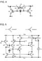
- Fig. 4 is a diagram illustrating the circuit configuration of an active inductor according to Example 3 of the invention. This active inductor comprises four transistors including MOSFETs M1, M3 and PMOSFETs M2, M4, and a single capacitor. That is, a pair of circuits as shown in Fig. 3 are combined together to constitute a differential active inductor with a floating capacitor C.
- This differential active inductor has an inductance which is electrically controllable by changing the transconductance of the MOSFET.
- The active inductors according to the present invention can be implemented in any semiconductor integrated processes. However, the maximum operating frequency of any of these circuits of the active inductors is limited by the maximum operating frequency of the MOSFETs and parasitic capacitances. Therefore, a CMOS process with high frequency transistors (cut-off frequency ft: 20GHz) is required for applications to high frequency circuits (e.g., RF to 2GHz). Formation of a CMOS on an SOI (silicon-on-insulator) substrate is very advantageous in that source-drain junction capacitances are reduced.
- Fig. 5 is a diagram illustrating the circuit configuration of an active inductor according to Example 4 of the invention. The circuit configuration shown in Fig. 5 is a modification of the circuit configuration of Fig. 2, and includes a DC bias circuit. This active inductor comprises 13 transistors including NMOSFETs M1, M2, M4, M5, M6, M6, M8, M10, M11 and PMOSFETs M3, M7, M9, M12, M13, and a single capacitor.
- The NMOSFETs M1, M2 and the PMOSFET M3 are core transistors (corresponding to the three MOSFETs shown in Fig. 2) which determine the inductance.
- The NMOSFET M10 is cascade-connected in series to the NMOSFET M1 to increase its output resistance ro. The NMOSFET M4 is used to set the DC bias point of the NMOSFET M2 and the PMOSFET M3.
- The PMOSFETs M12, M13 constitute a current mirror circuit to set the bias current via the NMOSFET M5 for the NMOSFETs M4, M6, and via the PMOSFET M9 for the NMOSFET M1. It is noted that Io is an external bias current.
- At low frequencies, the drain-source resistance rds4 of the NMOSFET M4 limits the output impedance. The output resistance ro of this circuit is given by the following expression:
- The output node of the circuit is denoted by Vo. The circuit configuration shown in Fig. 5 is merely an example which may be employed for relatively low frequency applications, and all the bias transistor network is of course included for integration in a CMOS process. For simplification of the circuit, the bias circuit can also be implemented with the use of passive components (e.g., resistors).
- Fig. 6 is a graph illustrating an output impedance characteristic of the active inductor of Example 4 with respect to the frequency. The output impedance Zo (measured value) at the node Vo is shown as a function of the frequency.
- The active inductor having the circuit configuration shown in Fig. 5 and the output impedance characteristic shown in Fig. 6 is designed to be operative with an inductance of L=10µH. The circuit is implemented with the use of a capacitor having a capacitance of C=10pF. As a result, a resonant peak is observed at ωo∼20MHz. The output impedance Zo of the circuit is approximately 25Ω.
- With this circuit configuration, the inductance is determined by the transconductance of the transistors, the bias current and the capacitance of the capacitor C. The formation of the capacitor C can be achieved by utilizing a double-polysilicon capacitor process.
- The frequency response and the inductance are adjusted by changing the bias current Io.
- The active inductors according to the present invention are each implemented by employing a circuit configuration including at least one MOSFET and a single capacitor C. As compared with the conventional circuit configurations and the conventional passive components for the inductors, the following effects are noted.
- (1) The area of the circuit can be reduced as compared with passive components.
- (2) The inductance can be increased.
- (3) The inductance can electrically be varied. This is important for tuning and for correction for process fluctuations.
- (4) The number of constituent components can be reduced.
- (5) The operating frequency range can be extended by using high frequency MOS transistors and by using an SOI substrate for reduction of the parasitic capacitance.
-
- The active inductors according to the present invention each have an excellent frequency response characteristic and a reduced size as compared with the conventional active inductors.
Claims (9)
- An active inductor comprising:an MOSFET having a gate, a drain serving as an output terminal and a grounded source, the MOSFET having a transconductance gm1; anda capacitor having opposite ends, one of which is grounded and the other of which is connected to the gate of the MOSFET and to a voltage-controlled constant current source having a transconductance gm, the capacitor having a capacitance C;the active inductor being operative with a small-signal output impedance Zo between the output terminal and the ground expressed as Zo=jω {C/(gm1·gm)} (wherein ω is an angular frequency) and with an inductance Leq expressed as Leq={C/(gm1· gm)}.
- An active inductor as set forth in claim 1, wherein the inductance Leq is electrically varied by adjusting the transconductance gm of the voltage-controlled constant current source.
- An active inductor as set forth in claim 1, wherein the inductance Leq is electrically varied by adjusting the transconductance gml of the MOSFET.
- An active inductor as set forth in claim 1, wherein the voltage-controlled constant current source comprises an NMOSFET and a PMOSFET cascade-connected to each other, and each having a gate, a drain and a source, the drain of the NMOSFET being kept at a fixed potential, the gate of the NMOSFET being connected to the drain of the MOSFET, the source of the NMOSFET being connected to the source of the PMOSFET, the gate of the PMOSFET being connected to a variable potential, the drain of the PMOSFET being connected to the gate of the MOSFET.
- An active inductor as set forth in claim 1, wherein the voltage-controlled constant current source comprises a PMOSFET having a source connected to the drain of the MOSFET, a gate connected to a variable potential, and a drain connected to the gate of the MOSFET.
- An active inductor comprising:two NMOSFETs each having a gate, a drain serving as an output terminal and a grounded source;two PMOSFETs each having a gate, a drain and a source, the gates thereof being connected together to a DC potential, the sources thereof being respectively connected to the drains of the NMOSFETs; anda single capacitor having opposite ends respectively connected to the gates of the NMOSFETs.
- An active inductor as set forth in claim 6, which has an inductance which is electrically varied by adjusting a transconductance of the two PMOSFETs.
- An active inductor as set forth in claim 6, which has an inductance which is electrically varied by adjusting a DC voltage to be applied to the gates of the two PMOSFETs.
- An active inductor in which a MOSFET has its source/drain path connected between ground and output and its gate jointly connected to one end of a capacitance and to a voltage-controlled constant current source.
Applications Claiming Priority (2)
| Application Number | Priority Date | Filing Date | Title |
|---|---|---|---|
| JP2000042949 | 2000-02-21 | ||
| JP2000042949A JP3599627B2 (en) | 2000-02-21 | 2000-02-21 | Active inductor |
Publications (2)
| Publication Number | Publication Date |
|---|---|
| EP1128554A2 true EP1128554A2 (en) | 2001-08-29 |
| EP1128554A3 EP1128554A3 (en) | 2002-07-17 |
Family
ID=18565947
Family Applications (1)
| Application Number | Title | Priority Date | Filing Date |
|---|---|---|---|
| EP01301553A Withdrawn EP1128554A3 (en) | 2000-02-21 | 2001-02-21 | Active inductor |
Country Status (6)
| Country | Link |
|---|---|
| US (1) | US6515560B1 (en) |
| EP (1) | EP1128554A3 (en) |
| JP (1) | JP3599627B2 (en) |
| KR (1) | KR100402706B1 (en) |
| CN (1) | CN1184739C (en) |
| TW (1) | TW483237B (en) |
Cited By (3)
| Publication number | Priority date | Publication date | Assignee | Title |
|---|---|---|---|---|
| WO2009077856A3 (en) * | 2007-12-14 | 2009-08-13 | Acp Advanced Circuit Pursuit A | Variable inductor |
| EP2854287B1 (en) * | 2013-08-28 | 2020-06-24 | Analog Devices, Inc. | High speed amplifier |
| CN111884622A (en) * | 2020-07-06 | 2020-11-03 | 北京工业大学 | Differential active inductor working in wide frequency band |
Families Citing this family (20)
| Publication number | Priority date | Publication date | Assignee | Title |
|---|---|---|---|---|
| US7020450B2 (en) * | 2000-09-05 | 2006-03-28 | Nec Corporation | Active inductors using bipolar silicon transistors |
| JP4481590B2 (en) * | 2003-05-15 | 2010-06-16 | ルネサスエレクトロニクス株式会社 | Active inductance circuit and differential amplifier circuit |
| US7199685B2 (en) * | 2004-08-30 | 2007-04-03 | Agere Systems Inc. | Three-terminal, tunable active inductor |
| US7453315B2 (en) * | 2006-04-26 | 2008-11-18 | Infineon Technologies Ag | Active inductive load that enhances circuit bandwidth |
| US7639079B2 (en) | 2007-02-09 | 2009-12-29 | Agere Systems Inc. | Techniques for designing wide band low noise amplifiers |
| CN101174821B (en) * | 2007-09-27 | 2010-08-25 | 复旦大学 | Adjustable active inductance irrespective to temperature and supply voltage |
| CN101197560B (en) * | 2007-12-27 | 2011-06-22 | 复旦大学 | Medium Frequency LC Parallel Resonant Circuit Using Active Inductor |
| US7889004B1 (en) | 2009-09-30 | 2011-02-15 | Analog Devices, Inc. | Operational amplifiers with enhanced parameters |
| CN102013868B (en) * | 2010-11-30 | 2013-11-20 | 中山大学 | Numerical control variable inductance |
| CN102111123B (en) * | 2011-01-07 | 2013-06-19 | 清华大学 | Suspension difference active inducer based on positive feedback |
| CN102142829B (en) * | 2011-02-25 | 2013-07-24 | 清华大学 | Positive feedback-based suspension differential active inductor |
| ITMI20112243A1 (en) * | 2011-12-12 | 2013-06-13 | Uni Degli Studi Dell A Quila | ELECTRONIC CIRCUIT WITH LOW NOISE SIMULATING THE BEHAVIOR OF AN INDUCTANCE |
| JP6036564B2 (en) * | 2013-06-14 | 2016-11-30 | 富士通株式会社 | Variable inductor circuit and high frequency circuit |
| CN103414466B (en) * | 2013-08-08 | 2016-01-20 | 南京邮电大学 | A kind of annular voltage controlled oscillator of high speed |
| US9312819B1 (en) * | 2015-03-24 | 2016-04-12 | Global Unichip Corporation | Active inductor and associated amplifying circuit |
| JP6740122B2 (en) * | 2016-12-28 | 2020-08-12 | キオクシア株式会社 | Active inductor and amplifier circuit |
| CN108768342B (en) * | 2018-05-31 | 2021-09-03 | 北京工业大学 | Radio frequency integrated active inductor |
| US20200081467A1 (en) * | 2018-09-07 | 2020-03-12 | Qualcomm Incorporated | Gyrator-based low-dropout (ldo) regulator |
| EP4154400A1 (en) * | 2020-05-20 | 2023-03-29 | Telefonaktiebolaget LM ERICSSON (PUBL) | A filter circuitry using active inductor |
| CN111917381B (en) * | 2020-08-11 | 2024-10-15 | 深圳市时代速信科技有限公司 | Low-noise amplifier based on active inductor |
Citations (1)
| Publication number | Priority date | Publication date | Assignee | Title |
|---|---|---|---|---|
| JPH02205107A (en) * | 1989-02-02 | 1990-08-15 | A T R Koudenpa Tsushin Kenkyusho:Kk | Active inductor |
Family Cites Families (4)
| Publication number | Priority date | Publication date | Assignee | Title |
|---|---|---|---|---|
| JPS63219150A (en) | 1987-03-07 | 1988-09-12 | A T R Hikari Denpa Tsushin Kenkyusho:Kk | Active inductor |
| JP3204481B2 (en) | 1994-12-27 | 2001-09-04 | 日本電信電話株式会社 | Active inductor |
| JP3216693B2 (en) | 1995-02-01 | 2001-10-09 | 日本電信電話株式会社 | Active inductor |
| KR100265761B1 (en) * | 1997-12-08 | 2000-09-15 | 윤종용 | Active inductor |
-
2000
- 2000-02-21 JP JP2000042949A patent/JP3599627B2/en not_active Expired - Fee Related
-
2001
- 2001-02-05 US US09/775,587 patent/US6515560B1/en not_active Expired - Fee Related
- 2001-02-08 TW TW090102788A patent/TW483237B/en not_active IP Right Cessation
- 2001-02-21 CN CNB011047526A patent/CN1184739C/en not_active Expired - Fee Related
- 2001-02-21 KR KR10-2001-0008680A patent/KR100402706B1/en not_active Expired - Fee Related
- 2001-02-21 EP EP01301553A patent/EP1128554A3/en not_active Withdrawn
Patent Citations (1)
| Publication number | Priority date | Publication date | Assignee | Title |
|---|---|---|---|---|
| JPH02205107A (en) * | 1989-02-02 | 1990-08-15 | A T R Koudenpa Tsushin Kenkyusho:Kk | Active inductor |
Non-Patent Citations (3)
| Title |
|---|
| ANONYMOUS: "Polarized Capacitor Mounting", IBM TECHNICAL DISCLOSURE BULLETIN, vol. 28, no. 3, 1 August 1985 (1985-08-01), New York, US, pages 940 - 941 * |
| HARA S ET AL: "Broad band monolithic microwave active inductor and application to a miniaturized wide band amplifier", 19880524; 19880524 - 19880525, 24 May 1988 (1988-05-24), pages 117 - 120, XP010076526 * |
| KLUMPERINK E.A.M.: "A Systematic Approach to Circuit Design and Analysis: Classification of Two-VCCS Circuits", IEEE TRANSACTIONS ON CIRCUITS AND SYSTEMS I: FUNDAMENTAL THEORY AND APPLICATIONS, IEEE INC. NEW YORK, US, vol. 46, no. 7, 1 July 1999 (1999-07-01), NEW YORK, US, pages 810 - 819, XP011011925 * |
Cited By (7)
| Publication number | Priority date | Publication date | Assignee | Title |
|---|---|---|---|---|
| WO2009077856A3 (en) * | 2007-12-14 | 2009-08-13 | Acp Advanced Circuit Pursuit A | Variable inductor |
| CN101904096A (en) * | 2007-12-14 | 2010-12-01 | Acp尖端电路钻研股份公司 | Variable inductor |
| US8253504B2 (en) | 2007-12-14 | 2012-08-28 | ACP Advanced Circuit Purcuit AG | Electronically variable oscillator |
| CN101904096B (en) * | 2007-12-14 | 2014-05-28 | Acp尖端电路钻研股份公司 | Variable inductor |
| EP2854287B1 (en) * | 2013-08-28 | 2020-06-24 | Analog Devices, Inc. | High speed amplifier |
| CN111884622A (en) * | 2020-07-06 | 2020-11-03 | 北京工业大学 | Differential active inductor working in wide frequency band |
| CN111884622B (en) * | 2020-07-06 | 2022-12-23 | 北京工业大学 | Differential active inductor working in wide frequency band |
Also Published As
| Publication number | Publication date |
|---|---|
| TW483237B (en) | 2002-04-11 |
| KR20010083228A (en) | 2001-08-31 |
| US6515560B1 (en) | 2003-02-04 |
| CN1312613A (en) | 2001-09-12 |
| KR100402706B1 (en) | 2003-10-22 |
| JP3599627B2 (en) | 2004-12-08 |
| JP2001237672A (en) | 2001-08-31 |
| CN1184739C (en) | 2005-01-12 |
| EP1128554A3 (en) | 2002-07-17 |
Similar Documents
| Publication | Publication Date | Title |
|---|---|---|
| US6515560B1 (en) | Active inductor | |
| KR101071599B1 (en) | - self-biased voltage controlled oscillator | |
| US7679446B2 (en) | Variable-gain low-noise amplifier | |
| CN101834567B (en) | Broadband gain adjustable low-noise amplifier | |
| Uyanik et al. | Compact low voltage high-Q CMOS active inductor suitable for RF applications | |
| US9935583B2 (en) | Power amplifier circuit | |
| US7253707B2 (en) | Tunable active inductor | |
| Manjula et al. | Design of low power low noise tunable active inductors for multiband RF front end communication circuits | |
| Pascht et al. | A CMOS low noise amplifier at 2.4 GHz with active inductor load | |
| KR101043668B1 (en) | Active inductor | |
| Ben Hammadi et al. | RF and microwave reconfigurable bandpass filter design using optimized active inductor circuit | |
| Thanachayanont | A 1.5-V high-Q CMOS active inductor for IF/RF wireless applications | |
| US7123899B1 (en) | Broadband single-ended input upconverter | |
| JP3474750B2 (en) | High frequency integrated circuit device and frequency conversion circuit device | |
| US9374065B2 (en) | Variable inductor circuit and high frequency circuit | |
| Chang et al. | A 900 MHz active CMOS LNA with a bandpass filter | |
| US20070103235A1 (en) | Inductorless broadband RF low noise amplifier | |
| JPH11205055A (en) | Variable gain differential amplifier circuit | |
| CN111446930A (en) | Radio frequency inductance circuit | |
| JP7669773B2 (en) | Semiconductor Device | |
| JP2639808B2 (en) | Active filter | |
| JP3204481B2 (en) | Active inductor | |
| JP2718378B2 (en) | Semiconductor amplifier circuit | |
| TW463457B (en) | Novel technique to generate negative conductance in CMOS tuned cascode RF amplifiers | |
| KR0114558Y1 (en) | Active inductor circuit |
Legal Events
| Date | Code | Title | Description |
|---|---|---|---|
| PUAI | Public reference made under article 153(3) epc to a published international application that has entered the european phase |
Free format text: ORIGINAL CODE: 0009012 |
|
| AK | Designated contracting states |
Kind code of ref document: A2 Designated state(s): AT BE CH CY DE DK ES FI FR GB GR IE IT LI LU MC NL PT SE TR |
|
| AX | Request for extension of the european patent |
Free format text: AL;LT;LV;MK;RO;SI |
|
| PUAL | Search report despatched |
Free format text: ORIGINAL CODE: 0009013 |
|
| AK | Designated contracting states |
Kind code of ref document: A3 Designated state(s): AT BE CH CY DE DK ES FI FR GB GR IE IT LI LU MC NL PT SE TR |
|
| AX | Request for extension of the european patent |
Free format text: AL;LT;LV;MK;RO;SI |
|
| 17P | Request for examination filed |
Effective date: 20021018 |
|
| AKX | Designation fees paid |
Designated state(s): DE FR GB IT NL |
|
| 17Q | First examination report despatched |
Effective date: 20050209 |
|
| 17Q | First examination report despatched |
Effective date: 20050209 |
|
| STAA | Information on the status of an ep patent application or granted ep patent |
Free format text: STATUS: THE APPLICATION IS DEEMED TO BE WITHDRAWN |
|
| 18D | Application deemed to be withdrawn |
Effective date: 20110516 |