EP1128551A2 - Curing method for silicone rubber and apparatus for the same - Google Patents
Curing method for silicone rubber and apparatus for the same Download PDFInfo
- Publication number
- EP1128551A2 EP1128551A2 EP00128150A EP00128150A EP1128551A2 EP 1128551 A2 EP1128551 A2 EP 1128551A2 EP 00128150 A EP00128150 A EP 00128150A EP 00128150 A EP00128150 A EP 00128150A EP 1128551 A2 EP1128551 A2 EP 1128551A2
- Authority
- EP
- European Patent Office
- Prior art keywords
- silicone rubber
- jig
- electronic components
- far infrared
- infrared rays
- Prior art date
- Legal status (The legal status is an assumption and is not a legal conclusion. Google has not performed a legal analysis and makes no representation as to the accuracy of the status listed.)
- Granted
Links
- 229920002379 silicone rubber Polymers 0.000 title claims abstract description 98
- 239000004945 silicone rubber Substances 0.000 title claims abstract description 98
- 238000001723 curing Methods 0.000 title claims description 60
- 238000000034 method Methods 0.000 claims abstract description 22
- 230000001678 irradiating effect Effects 0.000 claims description 8
- 238000000576 coating method Methods 0.000 claims description 7
- 239000011248 coating agent Substances 0.000 claims description 5
- 239000003822 epoxy resin Substances 0.000 claims description 5
- 229920000647 polyepoxide Polymers 0.000 claims description 5
- 239000000463 material Substances 0.000 claims description 4
- 239000011810 insulating material Substances 0.000 claims description 2
- 238000010438 heat treatment Methods 0.000 abstract description 11
- 230000015556 catabolic process Effects 0.000 abstract description 3
- 238000006731 degradation reaction Methods 0.000 abstract description 3
- 230000002093 peripheral effect Effects 0.000 abstract description 3
- 229920005989 resin Polymers 0.000 description 11
- 239000011347 resin Substances 0.000 description 11
- 238000000862 absorption spectrum Methods 0.000 description 6
- 238000010521 absorption reaction Methods 0.000 description 5
- 238000001816 cooling Methods 0.000 description 5
- 230000001965 increasing effect Effects 0.000 description 4
- 239000000843 powder Substances 0.000 description 4
- XAGFODPZIPBFFR-UHFFFAOYSA-N aluminium Chemical compound [Al] XAGFODPZIPBFFR-UHFFFAOYSA-N 0.000 description 3
- 239000000919 ceramic Substances 0.000 description 3
- 238000007598 dipping method Methods 0.000 description 3
- 230000000694 effects Effects 0.000 description 3
- 230000003028 elevating effect Effects 0.000 description 3
- 239000010410 layer Substances 0.000 description 3
- 238000004519 manufacturing process Methods 0.000 description 3
- 239000003570 air Substances 0.000 description 2
- 230000005540 biological transmission Effects 0.000 description 2
- 238000013016 damping Methods 0.000 description 2
- 239000000758 substrate Substances 0.000 description 2
- 238000002835 absorbance Methods 0.000 description 1
- 229910052782 aluminium Inorganic materials 0.000 description 1
- 239000012080 ambient air Substances 0.000 description 1
- 238000010073 coating (rubber) Methods 0.000 description 1
- 230000000593 degrading effect Effects 0.000 description 1
- 239000013013 elastic material Substances 0.000 description 1
- 238000012986 modification Methods 0.000 description 1
- 230000004048 modification Effects 0.000 description 1
- 229920001296 polysiloxane Polymers 0.000 description 1
- 230000000452 restraining effect Effects 0.000 description 1
- 239000002356 single layer Substances 0.000 description 1
- 229920001187 thermosetting polymer Polymers 0.000 description 1
Images



Classifications
-
- B—PERFORMING OPERATIONS; TRANSPORTING
- B05—SPRAYING OR ATOMISING IN GENERAL; APPLYING FLUENT MATERIALS TO SURFACES, IN GENERAL
- B05D—PROCESSES FOR APPLYING FLUENT MATERIALS TO SURFACES, IN GENERAL
- B05D3/00—Pretreatment of surfaces to which liquids or other fluent materials are to be applied; After-treatment of applied coatings, e.g. intermediate treating of an applied coating preparatory to subsequent applications of liquids or other fluent materials
- B05D3/06—Pretreatment of surfaces to which liquids or other fluent materials are to be applied; After-treatment of applied coatings, e.g. intermediate treating of an applied coating preparatory to subsequent applications of liquids or other fluent materials by exposure to radiation
-
- H—ELECTRICITY
- H03—ELECTRONIC CIRCUITRY
- H03H—IMPEDANCE NETWORKS, e.g. RESONANT CIRCUITS; RESONATORS
- H03H3/00—Apparatus or processes specially adapted for the manufacture of impedance networks, resonating circuits, resonators
- H03H3/007—Apparatus or processes specially adapted for the manufacture of impedance networks, resonating circuits, resonators for the manufacture of electromechanical resonators or networks
- H03H3/02—Apparatus or processes specially adapted for the manufacture of impedance networks, resonating circuits, resonators for the manufacture of electromechanical resonators or networks for the manufacture of piezoelectric or electrostrictive resonators or networks
-
- B—PERFORMING OPERATIONS; TRANSPORTING
- B29—WORKING OF PLASTICS; WORKING OF SUBSTANCES IN A PLASTIC STATE IN GENERAL
- B29C—SHAPING OR JOINING OF PLASTICS; SHAPING OF MATERIAL IN A PLASTIC STATE, NOT OTHERWISE PROVIDED FOR; AFTER-TREATMENT OF THE SHAPED PRODUCTS, e.g. REPAIRING
- B29C35/00—Heating, cooling or curing, e.g. crosslinking or vulcanising; Apparatus therefor
- B29C35/02—Heating or curing, e.g. crosslinking or vulcanizing during moulding, e.g. in a mould
- B29C35/08—Heating or curing, e.g. crosslinking or vulcanizing during moulding, e.g. in a mould by wave energy or particle radiation
-
- C—CHEMISTRY; METALLURGY
- C08—ORGANIC MACROMOLECULAR COMPOUNDS; THEIR PREPARATION OR CHEMICAL WORKING-UP; COMPOSITIONS BASED THEREON
- C08J—WORKING-UP; GENERAL PROCESSES OF COMPOUNDING; AFTER-TREATMENT NOT COVERED BY SUBCLASSES C08B, C08C, C08F, C08G or C08H
- C08J7/00—Chemical treatment or coating of shaped articles made of macromolecular substances
- C08J7/12—Chemical modification
- C08J7/16—Chemical modification with polymerisable compounds
- C08J7/18—Chemical modification with polymerisable compounds using wave energy or particle radiation
Definitions
- the present invention relates to an apparatus for curing silicone rubber used with piezoelectric components or other electronic components, wherein after the periphery of piezoelectric element is covered with silicone rubber, the surrounding areas thereof are covered with an armoring resin.
- a conventional piezoelectric component is disclosed in Japanese Unexamined Patent Application Publication No. 1-228310, for example, wherein the periphery of a piezoelectric element having lead terminals attached thereto is covered with an elastic material such as silicone rubber and surroundings thereof are sealed with an armoring resin.
- the silicone rubber prevents changes in vibration characteristics of the piezoelectric element due to the contractile stress of the armoring resin and a damping effect on the restraining waveform distortion of the piezoelectric element as well.
- piezoelectric elements are attached to a lead frame, the periphery of the piezoelectric element is coated with silicone rubber by dipping it such that the lead frame is held by a jig so as to be heated and cured in an oven, then an epoxy resin is coated therearound by dipping it such that the lead frame is held by the jig so as to be heated and cured again in an oven and so as to define an armoring resin layer. Then the lead frame is removed from the jig and the piezoelectric component is obtained by separating lead terminals from the lead frame. In such a manner, mass-productivity is increased and uniform quality of the products is obtained as well by subjecting a plurality of piezoelectric elements, which are continued to be held by the jig, to the series of processes.
- thermosetting silicone rubber When the thermosetting silicone rubber is heated and cured in an oven, it is generally heated at a temperature in a range of 150°C to 160°C range, for 30 minutes to 1 hour by utilizing direct heat transmission of hot air.
- a piezoelectric element a piezoelectric ceramic element, for example
- piezoelectric characteristics are degraded (dipole).
- the silicone rubber coating and the armoring resin forming processes are performed while a plurality of piezoelectric elements are held on a jig as described above, during the heating and curing in an oven, the jig as well as piezoelectric elements must be heated because the jig holding the piezoelectric elements is inserted into the oven. Since the thermal capacity of the jig is much greater than the thermal capacity of the piezoelectric elements, the jig requires a heating time and it also requires a cooling time after being removed from the oven, so that there is a problem that a long time is required for the curing process of the silicone rubber.
- the equipment in the conventional heating and curing apparatus having a heater and a fan, the equipment must be relatively scale, resulting in a problem of high cost when including a conveying system.
- preferred embodiments of the present invention provide a curing method and a curing apparatus wherein heating and curing processes are performed very quickly and without degrading the characteristics of the piezoelectric element so as to improve productivity of electronic component manufacturing.
- a method of curing silicone rubber includes the steps of holding a plurality of piezoelectric elements in a jig, coating silicone rubber on external surfaces of the piezoelectric elements held by the jig, and irradiating the uncured silicone rubber coated on the external surfaces of the piezoelectric elements with far infrared rays so as to cure the silicone rubber.
- a curing apparatus for silicone rubber for curing the silicone rubber coated on external surfaces of electronic components such as piezoelectric elements
- the curing apparatus including a jig for holding the piezoelectric elements having the uncured silicone rubber coated on the external surfaces thereof, and having the property of reflecting far infrared rays, and a far-infrared-ray generating unit for irradiating the uncured silicone rubber coated on the external surfaces of the piezoelectric elements with far infrared rays so as to cure the silicone rubber.
- the jig is transported to a far infrared generating unit.
- the piezoelectric elements are irradiated with far infrared rays generated in the far infrared generating unit, the far infrared rays are selectively absorbed into the silicone rubber coated on the electronic components while they are not substantially absorbed in the jig and the electronic components. Therefore, the electronic components, e.g., piezoelectric elements do not produce heat, and degradation (dipole) of piezoelectric characteristics is thereby prevented.
- the jig having a large thermal capacity does not produce heat, so that the time for heating and the period for cooling after the curing process is greatly reduced. Since in the silicone rubber, heat is produced from the inside thereof by far infrared rays, the curing proceeds evenly, so that the entire silicone rubber can be uniformly cured.
- the far infrared rays emitted from the far infrared generating unit include wavelengths of about 7 to about 15 ⁇ m.
- the range of the wavelengths is generally 5 ⁇ m to 1000 ⁇ m, and among the wavelengths, the absorption spectrum of the silicone rubber exhibits the highest level in the wavelengths of about 7 ⁇ m to about 15 ⁇ m.
- the far infrared rays can be effectively absorbed into the silicone rubber while not being absorbed in the electronic components and jig, and the thermal efficiency is thereby improved.
- Fig. 1 is a longitudinal sectional view of an example of a piezoelectric element according to a preferred embodiment of the present invention
- Fig. 1 shows an example of a work W used in a curing apparatus for silicone rubber according to a preferred embodiment of the present invention.
- the work W is a piezoelectric component having lead terminals.
- the work W preferably includes a substantially rectangular piezoelectric element 1 including a shear mode vibration element, for example, and three lead terminals 2 to 4. Both end portions including at least both end edges of the piezoelectric element 1 having the lead terminals 2 to 4 adhered thereto are covered with a first silicone rubber 5
- the entire surroundings of the piezoelectric element 1 covered with the first silicone rubber 5 are covered with a second silicone rubber 6, and the entire surroundings thereof are further covered with an armoring resin 7 such as an epoxy resin.
- both end-edge portions which are most susceptible to a contractile stress of the armoring resin 7 are covered with double silicone rubber films 5 and 6, even when the contractile stress of the armoring resin 7 is changed due to changes in temperature and changes in the stress can be absorbed, resulting in solving the problem of changes in characteristics due to temperature. Also, the damping effect of the piezoelectric component W is secured by the second silicone rubber 6, so that the piezoelectric component W has a feature that waveform distortion is prevented from occurring.
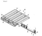
- the piezoelectric components W are aligned and held in a jig 10 such that a plurality of piezoelectric elements 1 are attached to a lead frame 8.
- the jig 10 used in a preferred embodiment is preferably the jig disclosed in Japanese Patent No. 2581342, for example, wherein on the top surfaces of non-magnetic hard substrates 11, a plurality of holding grooves 12 for holding strip portions of the lead frames 8 are formed, and wherein a plurality of magnetic lead frames 8 are arranged and absorbed in a line to be held by a magnet (not shown).
- the hard substrates 11 of the jig 10 are made of a lustrous metallic plate, such as an aluminum plate, having a property of reflecting far infrared rays.
- the piezoelectric components W held by the jig 10 as described above are subjected to a coating process of the first silicone rubber 5 after being coated with the first silicone rubber 5 by dripping. Then the work W is sent to an apparatus for curing silicone rubber, which will be described later, so that the uncured first silicone rubber 5 is heated and cured. Then the work W is subjected to a coating process of the second silicone rubber 6, after being coated with the second silicone rubber 6 by dipping, or other suitable process, it is again sent to the curing apparatus for silicone rubber, which will be described later, so that the uncured second silicone rubber 6 is heated and cured.
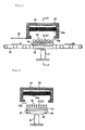
- Figs. 3 to 5 show an example of an apparatus for curing silicone rubber according to a preferred embodiment of the present invention.
- a conveyor 20 conveys the jig 10 carrying the works W therewith in the direction indicated by arrows.
- a pusher 22 is provided for being driven up-and-down by an elevating unit 21 such as a cylinder As shown in Fig. 4, the pusher 22 rises and falls between a pair of conveyors 20 so as to raise the jig 10 horizontally.
- a curing furnace 23 is provided over the elevating unit 21.
- the furnace wall of the curing furnace 23 is preferably made of a heat insulating material so as to prevent variations in the temperature of a heater 24, which will be described later.
- a jig-insertable opening 23a is formed on the bottom surface of the curing furnace 23.
- the far-infrared panel heater 24 having a heat-generating surface 24a facing downwardly is horizontally fixed thereto.
- the heat-generating surface 24a of the far-infrared panel heater 24 has a larger area than that of the jig 10.
- the wavelength of emitting far infrared rays is set in accordance with the absorption spectrum of the silicone rubber.
- a support member not shown) for supporting the bottom surfaces of side ends of the jig 10 is arranged inside the curing furnace 23.
- the support member is arranged to support the jig 10 horizontally relative to the heat-generating surface 24a of the far-infrared panel heater 24 by supporting the bottom surface of the jig 10 when the jig 10 is inserted inside the curing furnace 23 by the pusher 22
- a shutter 25 being opened and closed by a driver (not shown) is arranged.
- the shutter 25 is for closing the opening 23a of the curing furnace 23 so as to prevent ambient air from entering therein.
- the jig 10 placed on the conveyors 20 is conveyed in the direction of arrows so as to be stopped underneath the curing furnace 23. Then the jig 10 is raised from the conveyors 20 by the pusher 22, while the driver is driven and the shutter 25 is opened, so as to be inserted inside the curing furnace 23 from the opening 23a thereof.
- the bottom surface of the jig 10 is supported by the support member, so that the jig 10 is horizontally supported relative to the heat-generating surface 24a of the far-infrared panel heater 24. Then the shutter 25 closes the opening 23a of the curing furnace 23.
- the works W arranged on the jig 10 are irradiated with far infrared rays by the far-infrared panel heater 24 so as to cure the silicone rubber films 5 and 6 coated on the works W.
- the emitting far infrared rays include wavelengths of about 7 ⁇ m to about 15 pm, in particular, the silicone rubber films 5 and 6 can be efficiently heated substantially without heating the jig 10 and the piezoelectric components W.
- the shutter 25 is opened, the pusher 22 is elevated by the elevating unit 21 so as to support the bottom surface of the jig 10 in the curing furnace 23, the jig 10 is taken out from the curing furnace 23 by lowering the pusher 22, and the shutter 25 is closed. Then the jig 10 is placed on the conveyors 20 so as to be transferred in the direction of arrows by driving the conveyors 20.
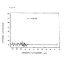
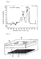
- Figs. 6 to 9 show measured results of characteristics in the infrared absorption of aluminum powder forming the jig 10, ceramic powder forming the piezoelectric component W, Sn powder forming the terminals 2 to 4, and the silicone rubber, respectively.
- the abscissa shows the wavelength of infrared rays while the ordinate shows the absorbance of the infrared rays.
- the silicone rubber has an absorption spectrum in the far infrared range (wavelengths of about 5 ⁇ m to about 1000 ⁇ m) In particular, in the range of about 7 ⁇ m to about 15 ⁇ m, peaks of the absorption spectrum exist. In contrast, other materials have scarcely the absorption spectrum in the far infrared range, so that they are difficult to be heated. Therefore, it is understood that when irradiated with far infrared rays, only the silicone rubber is selectively heated.
- the silicone rubber fully absorbs far infrared rays as described above, the temperature thereof can be efficiently increased within a short time. With an increasing raising rate of temperature, the curing time can be reduced. Since the temperature of only the silicone rubber is increased, the curing temperature of the silicone rubber can be very high, so that the curing time is greatly minimized.
- the jig 10 does not absorb far infrared rays well and the irradiating time of the far infrared rays is small, so that the jig 10 cannot be substantially heated. Therefore, the jig 10 can be continuously used as it is without cooling it, and the heating and curing times are greatly reduced.
- the far-infrared heater is simpler and more compact in structure than the oven, so that the productivity per unit area is improved.
- the far-infrared panel heater which is the essential element of the apparatus, is relatively inexpensive. Furthermore, the cooling device for the jig 10 can be omitted, resulting in reduction in equipment costs.
- the size of the heater is such that it is preferable to use a heater having a size that is larger than the area for heating the works, because the temperature of end portions of the heater is liable to be lowered due to the escaping of the heat in the lateral directions.
- the curing furnace 23 is constructed of an insulated structure so as to prevent the heat from escaping to the ambience to the utmost.
- the distance to the heater is also important. When the distance between the heater and the works W is too small, there are problems that variations in the heater temperature directly have an effect thereon, and the heat transmission through air exerts influence thereon. Conversely, when the works W are separated from the heater in the distance, although variations in the temperature are reduced, the thermal efficiency of the heater is reduced. Therefore, in view of these conditions, the distance must be properly determined.
- a piezoelectric component W having lead terminals and covered with double layers of silicone rubber is shown.
- the piezoelectric element may be covered with a single layer of silicone rubber.
- preferred embodiments of the present invention are more efficient because two steps of heating and curing are needed.
- preferred embodiments of the present invention can be applied to not only the piezoelectric component having lead terminals but also to a chip piezoelectric component W partially covered with silicone rubber S coated thereon.
- the piezoelectric component W may be conveyed by placing it on a planar jig H into the curing furnace 23 shown in Fig. 3.
- any other electronic component including silicone material can be used with the method and apparatus for curing silicone rubber of the present invention.
- the jig 10 is used in both curing processes of the first silicone rubber 5 and the second silicone rubber 6.
- the jig may be also used in the curing process of the armoring resin 7.
- the same infrared heater can be used for both curing processes of the silicone rubber and the armoring resin.
- the batch-type curing furnace 23 is shown, however, a continuous-type-curing furnace may be used. That is, a conveyor is continuously arranged from the inlet of the curing furnace toward the outlet thereof, so that the works W are heated by the far infrared heater while the jig is conveyed by the conveyor so as to cure the silicone rubber.
- the curing apparatus can cure the silicone rubber within a very short time, so that it is effective that it be applied to the continuous-type-curing furnace, which cannot hold the silicone rubber for a long time in the furnace.
- the piezoelectric element covered with the uncured silicone rubber is supported on the jig and the silicone rubber is irradiated with far infrared rays, so that the far infrared rays are selectively absorbed into the silicone rubber, and the silicone rubber is thereby cured in a short time.
- the far infrared rays cannot be substantially absorbed in the piezoelectric element, so that it does not produce heat, and the degradation of piezoelectric characteristics is also reliably prevented.
- the jig scarcely absorbs far infrared rays, so that it is not substantially heated because of the short irradiation time. Therefore, the jig can be continuously used as it is without cooling it, and the productivity is thereby improved.
- the curing proceeds evenly, so that the entire silicone rubber is uniformly cured.
Landscapes
- Health & Medical Sciences (AREA)
- Engineering & Computer Science (AREA)
- Chemical & Material Sciences (AREA)
- Manufacturing & Machinery (AREA)
- Physics & Mathematics (AREA)
- Toxicology (AREA)
- General Chemical & Material Sciences (AREA)
- Thermal Sciences (AREA)
- Oral & Maxillofacial Surgery (AREA)
- Plasma & Fusion (AREA)
- Chemical Kinetics & Catalysis (AREA)
- Medicinal Chemistry (AREA)
- Polymers & Plastics (AREA)
- Organic Chemistry (AREA)
- Heating, Cooling, Or Curing Plastics Or The Like In General (AREA)
- Processes Of Treating Macromolecular Substances (AREA)
- Application Of Or Painting With Fluid Materials (AREA)
- Encapsulation Of And Coatings For Semiconductor Or Solid State Devices (AREA)
Abstract
Description
Claims (20)
- A curing method for silicone rubber, comprising the steps of:holding a plurality of electronic components in a jig;coating silicone rubber on external surfaces of the electronic components held by the jig; andirradiating the uncured silicone rubber coated on the external surfaces of the electronic components with far infrared rays so as to cure the silicone rubber.
- A method according to Claim 1, wherein the far infrared rays include wavelengths of about 7 µm to about 15 µm.
- A method according to claim 1, wherein the electronic components are piezoelectric components.
- A method according to claim 1, wherein the electronic components include piezoelectric components having lead terminals.
- A method according to claim 1, wherein electronic components include substantially rectangular piezoelectric elements including shear mode vibration elements and a plurality of lead terminals.
- A method according to claim 5, wherein the lead terminals are covered by a first silicone rubber in the step of coating silicone rubber on external surfaces of the electronic components held by the jig.
- A method according to claim 6, wherein a second silicone rubber covering the entire area of the piezoelectric elements is applied in the step of coating silicone rubber on external surfaces of the electronic components held by the jig.
- A method according to claim 7, further comprising the step of coating an epoxy resin on the second silicone rubber so as to cover the entire area of the piezoelectric elements.
- A method according to claim 7, wherein the first silicone rubber is cured during the step of irradiating the uncured silicone rubber coated on the external surfaces of the electronic components before the second silicone rubber is applied.
- A method according to claim 1, wherein during the step of irradiating the uncured silicone rubber coated on the external surfaces of the electronic components with far infrared rays so as to cure the silicone rubber, the far infrared rays are not absorbed by the jig.
- An apparatus for curing silicone rubber coated on external surfaces of electronic components, the curing apparatus comprising:a jig arranged to holding the electronic components having uncured silicone rubber coated on external surfaces thereof, the jig having the property of reflecting far infrared rays; anda far-infrared-ray generating unit for irradiating the uncured silicone rubber coated on the external surfaces of the electronic componentswith far infrared rays so as to cure the silicone rubber.
- An apparatus according to Claim 11, wherein the far infrared rays emitted by the far-infrared-ray generating unit include wavelengths of about 7 µm to about 15 µm.
- An apparatus according to claim 11, wherein the electronic components are piezoelectric components.
- An apparatus according to claim 11, further comprising a conveyor arranged to transport the jig from a silicone rubber application unit to the far-infrared-ray generating unit.
- An apparatus according to claim 11, wherein the far infrared ray generating unit includes a curing furnace including a furnace wall made of a heat insulating material.
- An apparatus according to claim 11, wherein the far-infrared-ray generating unit includes a far-infrared panel heater having a heat-generating surface which has an area that is larger an area of the jig.
- An apparatus according to claim 11, wherein the jig is made of a material that does not absorb far infrared rays.
- An apparatus according to claim 11, wherein the jig is made of a material that is not heated in response to application of far infrared rays.
- An apparatus according to claim 11, wherein the electronic components include piezoelectric components having lead terminals.
- An apparatus according to claim 11, wherein electronic components include substantially rectangular piezoelectric elements including shear mode vibration elements and a plurality of lead terminals.
Applications Claiming Priority (2)
| Application Number | Priority Date | Filing Date | Title |
|---|---|---|---|
| JP2000042293 | 2000-02-21 | ||
| JP2000042293A JP3538707B2 (en) | 2000-02-21 | 2000-02-21 | Silicone rubber curing method and curing device |
Publications (3)
| Publication Number | Publication Date |
|---|---|
| EP1128551A2 true EP1128551A2 (en) | 2001-08-29 |
| EP1128551A3 EP1128551A3 (en) | 2003-12-10 |
| EP1128551B1 EP1128551B1 (en) | 2007-02-07 |
Family
ID=18565389
Family Applications (1)
| Application Number | Title | Priority Date | Filing Date |
|---|---|---|---|
| EP20000128150 Expired - Lifetime EP1128551B1 (en) | 2000-02-21 | 2000-12-21 | Curing method for silicone rubber and apparatus for the same |
Country Status (6)
| Country | Link |
|---|---|
| US (1) | US6440501B2 (en) |
| EP (1) | EP1128551B1 (en) |
| JP (1) | JP3538707B2 (en) |
| KR (1) | KR100491868B1 (en) |
| CN (1) | CN1309161C (en) |
| DE (1) | DE60033269D1 (en) |
Families Citing this family (11)
| Publication number | Priority date | Publication date | Assignee | Title |
|---|---|---|---|---|
| US5548206A (en) * | 1993-09-30 | 1996-08-20 | National Semiconductor Corporation | System and method for dual mode DC-DC power conversion |
| GB2383470B (en) * | 2001-11-12 | 2004-04-28 | Transense Technologies Plc | Self contained radio apparatus for transmission of data |
| US7616637B1 (en) | 2002-04-01 | 2009-11-10 | Cisco Technology, Inc. | Label switching in fibre channel networks |
| US7206288B2 (en) | 2002-06-12 | 2007-04-17 | Cisco Technology, Inc. | Methods and apparatus for characterizing a route in fibre channel fabric |
| US7433326B2 (en) | 2002-11-27 | 2008-10-07 | Cisco Technology, Inc. | Methods and devices for exchanging peer parameters between network devices |
| US7916628B2 (en) | 2004-11-01 | 2011-03-29 | Cisco Technology, Inc. | Trunking for fabric ports in fibre channel switches and attached devices |
| KR100962516B1 (en) * | 2008-11-14 | 2010-06-14 | 이만석 | Insulation surface treatment method of electrode using conductive silicon |
| CN104070623B (en) * | 2013-08-01 | 2016-06-01 | 上海威宁整形制品有限公司 | A kind of silicon rubber mammary prosthesis shell vulcanizing equipment |
| KR101689325B1 (en) | 2015-07-08 | 2016-12-23 | 주식회사 케이티 | Data security method and apparatus therefor |
| CN108291926B (en) * | 2015-12-04 | 2020-08-07 | 基斯特勒控股公司 | Accelerometer and method of making the same |
| CN108004899A (en) * | 2017-12-27 | 2018-05-08 | 翁毅 | System is quickly paved on a kind of road surface |
Family Cites Families (13)
| Publication number | Priority date | Publication date | Assignee | Title |
|---|---|---|---|---|
| US3836388A (en) * | 1972-10-18 | 1974-09-17 | Western Electric Co | Distributing a fluid evenly over the surface of an article |
| JPS6192026A (en) * | 1984-10-11 | 1986-05-10 | Matsushita Electric Ind Co Ltd | How to adjust delay time of surface wave delay line |
| JPS6196812A (en) * | 1984-10-17 | 1986-05-15 | Murata Mfg Co Ltd | Electronic component |
| JPH01228311A (en) | 1988-03-09 | 1989-09-12 | Murata Mfg Co Ltd | Production of piezoelectric resonator |
| JPH01228310A (en) * | 1988-03-09 | 1989-09-12 | Murata Mfg Co Ltd | Production of piezoelectric resonator |
| US4862827A (en) * | 1988-06-28 | 1989-09-05 | Wacker-Chemie Gmbh | Apparatus for coating semiconductor components on a dielectric film |
| JPH04208414A (en) * | 1990-11-30 | 1992-07-30 | Toto Ltd | Far infrared curing device for producing scagliola |
| US5240746A (en) * | 1991-02-25 | 1993-08-31 | Delco Electronics Corporation | System for performing related operations on workpieces |
| JPH08252914A (en) * | 1995-03-15 | 1996-10-01 | Seiko Epson Corp | Inkjet head and manufacturing method thereof |
| EP0847093A1 (en) * | 1995-08-25 | 1998-06-10 | Mitsui Chemicals, Inc. | Piezoelectric oscillator component, structure for supporting piezoelectric oscillator and method of mounting piezoelectric oscillator |
| JPH10154717A (en) | 1996-11-21 | 1998-06-09 | Nec Eng Ltd | Adhesive drying mechanism |
| US6323471B1 (en) * | 1998-11-25 | 2001-11-27 | Shunichi Yagi | Microwave and far infrared heating under reduced pressure |
| JP2000279875A (en) | 1999-03-31 | 2000-10-10 | Takaoka Kasei Kogyo Kk | Method for curing primer |
-
2000
- 2000-02-21 JP JP2000042293A patent/JP3538707B2/en not_active Expired - Lifetime
- 2000-12-21 EP EP20000128150 patent/EP1128551B1/en not_active Expired - Lifetime
- 2000-12-21 DE DE60033269T patent/DE60033269D1/en not_active Expired - Lifetime
- 2000-12-28 US US09/749,966 patent/US6440501B2/en not_active Expired - Lifetime
-
2001
- 2001-02-20 CN CNB011047232A patent/CN1309161C/en not_active Expired - Lifetime
- 2001-02-21 KR KR10-2001-0008614A patent/KR100491868B1/en not_active Expired - Lifetime
Also Published As
| Publication number | Publication date |
|---|---|
| CN1322058A (en) | 2001-11-14 |
| US6440501B2 (en) | 2002-08-27 |
| EP1128551B1 (en) | 2007-02-07 |
| KR100491868B1 (en) | 2005-05-27 |
| CN1309161C (en) | 2007-04-04 |
| JP3538707B2 (en) | 2004-06-14 |
| EP1128551A3 (en) | 2003-12-10 |
| US20010016233A1 (en) | 2001-08-23 |
| JP2001232649A (en) | 2001-08-28 |
| KR20010083215A (en) | 2001-08-31 |
| DE60033269D1 (en) | 2007-03-22 |
Similar Documents
| Publication | Publication Date | Title |
|---|---|---|
| EP1128551B1 (en) | Curing method for silicone rubber and apparatus for the same | |
| US7144471B2 (en) | Bonding method and apparatus | |
| JPH0621251A (en) | Semiconductor device having low temperature UV-curable epoxy encapsulation and manufacturing method thereof | |
| JP2002134762A (en) | Optical device and method of manufacturing the same | |
| KR20070033038A (en) | Method and device for mutual contact of two wafers | |
| US5993591A (en) | Coring of leadframes in carriers via radiant heat source | |
| EP0106564A1 (en) | A manufacturing method for a printed wiring substrate and a heater therefor | |
| RU2008126190A (en) | METHOD AND DEVICE FOR OBTAINING COMPONENT COMPOUND | |
| US6994544B2 (en) | Wafer scale thermal stress fixture and method | |
| JPH10340914A (en) | Method for manufacturing semiconductor device | |
| JPH09136055A (en) | Sealing agent curing method and curing apparatus | |
| KR100394487B1 (en) | semi-conductor protection package manufacturing device and method of manufacture it | |
| KR950002229B1 (en) | Equipment and method for hardening and pressing of lcd glass substrate | |
| JPH09136054A (en) | Heat curing device for sealant | |
| KR100368661B1 (en) | Vacuum hardening system for use in semiconductor packaging | |
| KR20050057122A (en) | A method and a device for bonding two plate-shaped objects | |
| JP5422043B2 (en) | Method of pretreating a frame or carrier element for producing a circuit board, and frame or carrier element and use therefor | |
| JP3751818B2 (en) | Sealing method of optical hollow semiconductor package | |
| JPH0639849A (en) | Post-curing apparatus | |
| JP2005158873A (en) | Manufacturing method of semiconductor device | |
| JP5128429B2 (en) | Compression molding apparatus and compression molding method using infrared irradiation member and infrared transmission block | |
| JP2006143876A (en) | Adhesive process, adhesion apparatus and compound product | |
| JPH1092852A (en) | Seal cure method and seal cure device | |
| KR20040056687A (en) | Cure apparatus having magazine | |
| JP2002033344A (en) | Semiconductor resin encapsulation and its manufacturing apparatus |
Legal Events
| Date | Code | Title | Description |
|---|---|---|---|
| PUAI | Public reference made under article 153(3) epc to a published international application that has entered the european phase |
Free format text: ORIGINAL CODE: 0009012 |
|
| 17P | Request for examination filed |
Effective date: 20001221 |
|
| AK | Designated contracting states |
Kind code of ref document: A2 Designated state(s): AT BE CH CY DE DK ES FI FR GB GR IE IT LI LU MC NL PT SE TR |
|
| AX | Request for extension of the european patent |
Free format text: AL;LT;LV;MK;RO;SI |
|
| PUAL | Search report despatched |
Free format text: ORIGINAL CODE: 0009013 |
|
| AK | Designated contracting states |
Kind code of ref document: A3 Designated state(s): AT BE CH CY DE DK ES FI FR GB GR IE IT LI LU MC NL PT SE TR |
|
| AX | Request for extension of the european patent |
Extension state: AL LT LV MK RO SI |
|
| RIC1 | Information provided on ipc code assigned before grant |
Ipc: 7H 03H 9/10 B Ipc: 7H 03H 3/02 A |
|
| AKX | Designation fees paid |
Designated state(s): DE FR GB |
|
| GRAP | Despatch of communication of intention to grant a patent |
Free format text: ORIGINAL CODE: EPIDOSNIGR1 |
|
| GRAS | Grant fee paid |
Free format text: ORIGINAL CODE: EPIDOSNIGR3 |
|
| GRAA | (expected) grant |
Free format text: ORIGINAL CODE: 0009210 |
|
| AK | Designated contracting states |
Kind code of ref document: B1 Designated state(s): DE FR GB |
|
| REG | Reference to a national code |
Ref country code: GB Ref legal event code: FG4D |
|
| REF | Corresponds to: |
Ref document number: 60033269 Country of ref document: DE Date of ref document: 20070322 Kind code of ref document: P |
|
| RAP2 | Party data changed (patent owner data changed or rights of a patent transferred) |
Owner name: MURATA MANUFACTURING CO., LTD. |
|
| EN | Fr: translation not filed | ||
| PLBE | No opposition filed within time limit |
Free format text: ORIGINAL CODE: 0009261 |
|
| STAA | Information on the status of an ep patent application or granted ep patent |
Free format text: STATUS: NO OPPOSITION FILED WITHIN TIME LIMIT |
|
| 26N | No opposition filed |
Effective date: 20071108 |
|
| PG25 | Lapsed in a contracting state [announced via postgrant information from national office to epo] |
Ref country code: DE Free format text: LAPSE BECAUSE OF FAILURE TO SUBMIT A TRANSLATION OF THE DESCRIPTION OR TO PAY THE FEE WITHIN THE PRESCRIBED TIME-LIMIT Effective date: 20070508 |
|
| PG25 | Lapsed in a contracting state [announced via postgrant information from national office to epo] |
Ref country code: FR Free format text: LAPSE BECAUSE OF FAILURE TO SUBMIT A TRANSLATION OF THE DESCRIPTION OR TO PAY THE FEE WITHIN THE PRESCRIBED TIME-LIMIT Effective date: 20070928 |
|
| PG25 | Lapsed in a contracting state [announced via postgrant information from national office to epo] |
Ref country code: FR Free format text: LAPSE BECAUSE OF FAILURE TO SUBMIT A TRANSLATION OF THE DESCRIPTION OR TO PAY THE FEE WITHIN THE PRESCRIBED TIME-LIMIT Effective date: 20070207 |
|
| PGFP | Annual fee paid to national office [announced via postgrant information from national office to epo] |
Ref country code: GB Payment date: 20191220 Year of fee payment: 20 |
|
| REG | Reference to a national code |
Ref country code: GB Ref legal event code: PE20 Expiry date: 20201220 |
|
| PG25 | Lapsed in a contracting state [announced via postgrant information from national office to epo] |
Ref country code: GB Free format text: LAPSE BECAUSE OF EXPIRATION OF PROTECTION Effective date: 20201220 |