EP1128173A2 - Capacitive semiconductor pressure sensor - Google Patents
Capacitive semiconductor pressure sensor Download PDFInfo
- Publication number
- EP1128173A2 EP1128173A2 EP00118286A EP00118286A EP1128173A2 EP 1128173 A2 EP1128173 A2 EP 1128173A2 EP 00118286 A EP00118286 A EP 00118286A EP 00118286 A EP00118286 A EP 00118286A EP 1128173 A2 EP1128173 A2 EP 1128173A2
- Authority
- EP
- European Patent Office
- Prior art keywords
- pressure
- capacitance
- ratio
- capacitance element
- sensor
- Prior art date
- Legal status (The legal status is an assumption and is not a legal conclusion. Google has not performed a legal analysis and makes no representation as to the accuracy of the status listed.)
- Withdrawn
Links
Images




Classifications
-
- G—PHYSICS
- G01—MEASURING; TESTING
- G01L—MEASURING FORCE, STRESS, TORQUE, WORK, MECHANICAL POWER, MECHANICAL EFFICIENCY, OR FLUID PRESSURE
- G01L9/00—Measuring steady of quasi-steady pressure of fluid or fluent solid material by electric or magnetic pressure-sensitive elements; Transmitting or indicating the displacement of mechanical pressure-sensitive elements, used to measure the steady or quasi-steady pressure of a fluid or fluent solid material, by electric or magnetic means
- G01L9/0041—Transmitting or indicating the displacement of flexible diaphragms
- G01L9/0072—Transmitting or indicating the displacement of flexible diaphragms using variations in capacitance
- G01L9/0073—Transmitting or indicating the displacement of flexible diaphragms using variations in capacitance using a semiconductive diaphragm
-
- H—ELECTRICITY
- H10—SEMICONDUCTOR DEVICES; ELECTRIC SOLID-STATE DEVICES NOT OTHERWISE PROVIDED FOR
- H10D—INORGANIC ELECTRIC SEMICONDUCTOR DEVICES
- H10D48/00—Individual devices not covered by groups H10D1/00 - H10D44/00
- H10D48/50—Devices controlled by mechanical forces, e.g. pressure
-
- G—PHYSICS
- G01—MEASURING; TESTING
- G01L—MEASURING FORCE, STRESS, TORQUE, WORK, MECHANICAL POWER, MECHANICAL EFFICIENCY, OR FLUID PRESSURE
- G01L9/00—Measuring steady of quasi-steady pressure of fluid or fluent solid material by electric or magnetic pressure-sensitive elements; Transmitting or indicating the displacement of mechanical pressure-sensitive elements, used to measure the steady or quasi-steady pressure of a fluid or fluent solid material, by electric or magnetic means
- G01L9/12—Measuring steady of quasi-steady pressure of fluid or fluent solid material by electric or magnetic pressure-sensitive elements; Transmitting or indicating the displacement of mechanical pressure-sensitive elements, used to measure the steady or quasi-steady pressure of a fluid or fluent solid material, by electric or magnetic means by making use of variations in capacitance, i.e. electric circuits therefor
- G01L9/125—Measuring steady of quasi-steady pressure of fluid or fluent solid material by electric or magnetic pressure-sensitive elements; Transmitting or indicating the displacement of mechanical pressure-sensitive elements, used to measure the steady or quasi-steady pressure of a fluid or fluent solid material, by electric or magnetic means by making use of variations in capacitance, i.e. electric circuits therefor with temperature compensating means
Definitions
- the present invention relates to a sensor for measuring a dynamic quantity by utilizing capacitance change, and more particularly to a semiconductor pressure sensor.
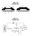
- JP-A-8-501156 which presents an electrostatic capacitance type pressure gauge manufactured through etching of a sacrificial layer, such as shown in Fig. 20.
- This pressure gauge is constituted of a pressure sensitive capacitance element 2 whose capacitance value changes with an applied pressure, and a reference capacitance element 3 although whose capacitance value is similar to that of the capacitance element 2 it does not change with the applied pressure.
- the structure and operation principle of this pressure gauge will be described.
- a fixed electrode 6 is formed on the surface of a silicon substrate 1, and a movable electrode 5 made of a polysilicon film is formed over the fixed electrode 6, with a space 7 being interposed therebetween.
- This space 7 was formed by etching and removing a sacrificial film formed in the space 7, through etch channels 12 partially formed through the variable electrode 5.
- a sealing film 9 made of a silicon oxide film is formed closing the etch channels 12.
- the space 7 in this state forms a pressure reference chamber which was vacuum sealed.
- This space 7, fixed electrode 6 formed on the substrate in the pressure reference chamber, and movable electrode 5 made of the polysilicon film, constitute a capacitor.
- the reference capacitance element 3 has a similar structure to that of the pressure sensitive capacitance element 2. However, the sealing film 9 on the variable electrode 5 of the reference capacitance element 3 is not removed to increase a diaphragm rigidity.
- variable electrode 5 of the pressure sensitive capacitance element 2 displaces by an amount corresponding to a difference between the external pressure and the pressure in the pressure reference chamber. Therefore, the gap between the variable electrode 5 and fixed electrode 6 changes and the capacitance changes. Since the reference capacitance element 3 has a high film rigidity, the variable electrode 5 will not be displaced by a pressure change and the capacitance thereof will not change.
- Cs 0 ⁇ Ss/d 0
- ⁇ the dielectric constant of a material in the electrode gap
- Ss the electrode area
- the difference ⁇ C between these two elements is converted into a voltage ⁇ V by a C-V converter circuit and amplified by and put out from an amplifier.
- FIG. 21 A first known example of the C-V converter circuit is described in JP-A-5-231973, and the circuit diagram thereof is shown in Fig. 21.
- This circuit is structured based upon a generally known switched capacitor circuit.
- the output changes with the capacitance difference of the pressure sensitive capacitance element 2 and reference capacitance element 3.
- the output voltage Vout is non-linear relative to the pressure P. This circuit is therefore associated with a problem that the output is required to be corrected in order to obtain a linear output.
- a pressure sensor used for controlling a vehicle engine is required to have a high pressure detection precision and high noise resistance.
- a high precision capacitance type C-V converter circuit like the second known example is therefore preferable to be adopted.
- it is effective to have a large output signal ⁇ V of the pressure gauge and lower the amplification factor of the amplifier, from the viewpoint of the S/N ratio.
- the C-V conversion efficiency is determined by the initial capacitance value ratio between those of the pressure sensitive capacitance element and the reference capacitance element, as indicated by the equation (6).
- this ratio has been set nearly to 1 and has not been used as a sensitivity adjustment parameter. Therefore, in order to have a large output of the pressure gauge, it is necessary to increase the displacement amount by lowering the diaphragm rigidity, or to increase the capacitance change AC itself by narrowing the electrode gap. However, lowering the diaphragm rigidity too much or narrowing the electrode gap may result in a contact between the diaphragm and the substrate in the range of the measuring pressure. The degree of design freedom is therefore limited.
- the present invention has been made to solve the above-described problems. It is an object of the invention to provide a pressure gauge of the type that a pressure is detected by using the capacitance ratio between the capacitance of a pressure sensitive capacitance element and that of a reference capacitance element, the pressure gauge being capable of increasing the C-V conversion efficiency and improving the sensor output S/N ratio by using a simple method.
- a semiconductor pressure sensor comprises: a pressure sensitive capacitance element having an electrostatic capacitance Cs changing with a pressure to be detected; a reference capacitance element having an electrostatic capacitance Cr not changing with the pressure; and means for detecting the pressure by outputting a signal corresponding to the ratio between the capacitances Cs and Cr, wherein the initial value Cr 0 of the capacitance Cr and the initial value Cs 0 of the capacitance Cs are defined by 1.2 ⁇ Cr 0 /Cs 0 ⁇ 1.8.
- Fig. 1 is a cross-sectional view of a semiconductor pressure sensor according to a first embodiment of the invention.
- Fig. 2 is a plan view of the semiconductor pressure sensor of the first embodiment.
- Fig. 3 is a cross-sectional view illustrating the operation principle of the semiconductor pressure sensor of the first embodiment.
- Fig. 4 is a diagram showing a capacitor-voltage conversion circuit using the semiconductor pressure sensor of the first embodiment.
- Fig. 5 is a timing chart illustrating the operation of the capacitor-voltage conversion circuit using the semiconductor pressure sensor of the first embodiment.
- Fig. 6 is a graph showing the relation between the Cr 0 /Cs 0 ratio, the output change after an endurance test, and the offset voltage.
- Fig. 7 is a cross-sectional view showing an example of the structure of a reference capacitance element of the semiconductor pressure sensor of the first embodiment.
- Fig. 8 is a cross-sectional view showing another example of the structure of the reference capacitance element of the semiconductor pressure sensor of the first embodiment.
- Fig. 9 is a cross-sectional view of a substrate illustrating a process step of manufacturing the semiconductor pressure sensor of the first embodiment.
- Fig. 10 is a cross-sectional view of a substrate illustrating another process step of manufacturing the semiconductor pressure sensor of the first embodiment.
- Fig. 11 is a cross-sectional view of a substrate illustrating another process step of manufacturing the semiconductor pressure sensor of the first embodiment.
- Fig. 12 is a cross-sectional view of a substrate illustrating another process step of manufacturing the semiconductor pressure sensor of the first embodiment.
- Fig. 13 is a cross-sectional view of a substrate illustrating another process step of manufacturing the semiconductor pressure sensor of the first embodiment.
- Fig. 14 is a cross-sectional view of a substrate illustrating another process step of manufacturing the semiconductor pressure sensor of the first embodiment.
- Fig. 15 is a cross-sectional view of a substrate illustrating another process step of manufacturing the semiconductor pressure sensor of the first embodiment.
- Fig. 16 is a cross-sectional view of a substrate illustrating another process step of manufacturing the semiconductor pressure sensor of the first embodiment.
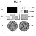
- Fig. 17 is a plan view of a semiconductor pressure sensor having a pressure gauge and an amplifier circuit according to a second embodiment of the invention.
- Fig. 18 is a cross-sectional view showing an example of mounting a semiconductor pressure sensor according to an embodiment of the invention.
- Fig. 19 is a diagram showing a vehicle engine control system using a semiconductor pressure sensor according to an embodiment of the invention.
- Fig. 20 is a cross-sectional view showing a conventional pressure sensitive capacitance element and a conventional reference capacitance element.
- Fig. 21 is a diagram of a conventional capacitance-voltage conversion circuit.
- Fig. 22 is a diagram of a conventional capacitance-voltage conversion circuit.
- FIG. 1 is a cross-sectional view of a semiconductor pressure sensor gauge according to the first embodiment of the invention
- Fig. 2 is a plan view of the semiconductor pressure sensor. The structure of the sensor will be described with reference to Figs. 1 and 2.
- a pressure sensitive capacitance element 2 On the surface of a silicon substrate 1, a pressure sensitive capacitance element 2, a reference capacitance element 3 and a capacitance-voltage conversion circuit 4 made of C-MOS (hereinafter called a C-V conversion circuit 4) are formed.
- the pressure sensitive capacitance element 2 has a fixed electrode 6 embedded in the upper surface layer of the substrate, and a movable electrode 5. These electrodes are disposed faced each other via a small space 7 to constitute a capacitance element structure. Formed on the variable electrode 5 are a sealing film 9 for vacuum sealing the inside of the small space 7 and a shielding and surface passivation film 10 formed on the sealing film 9.
- the structure of the reference capacitance element 3 is similar to that of the pressure sensitive capacitance element 2. However, in place of the variable electrode 5, a fixed electrode 8 with support columns is used to constitute the capacitance element whose capacitance will not change with an applied pressure.
- the diameter of the fixed electrode of the reference capacitance element 3 is made longer than that of the fixed electrode of the pressure sensitive capacitance element 2.
- Fig. 4 shows the structure of the C-V conversion circuit of an electrostatic capacitance type dynamic quantity sensor of this invention.
- a timing chart illustrating the operation of the embodiment is shown in Fig. 5.
- This embodiment is constituted of a pressure sensitive capacitance element 2, a reference capacitance element 3, constant voltage sources 111, 112, switches 121, 122, 123, 124, 131, and 132, a capacitor 106, an operational amplifier 107, an inverter 181, and an output terminal 109.
- the switches 121, 123 and 131 are driven by a drive signal ⁇ 1, and the switches 122, 124 and 132 are driven by an inverse phase drive signal ⁇ 1B.
- the inverter 181 multiplies an input signal by -1 and outputs it. This inverter 181 can be easily realized by a simple inverter amplifier using an operational amplifier, by a switched capacitor circuit, or by other circuits.
- Vout ⁇ (Cs - Cr)/Cf ⁇ Vcc
- Vout ⁇ 1 - (Cr/Cs) ⁇ Vcc
- the original object of differential output by using the pressure sensitive capacitance element and reference capacitance element is to eliminate a temperature-dependent change, manufacture variation, electromagnetic noises and the like.
- the absolute values of both Cr 0 and Cs 0 are made equal in order to make uniform the external disturbance influence degrees.
- the Cr 0 Cs 0 ratio is set to 1, there arises a problem of a large offset output (refer to the broken line in Fig. 6). This can be solved by adding an offset voltage adjusting circuit to the C-V converter circuit. Since the adjustment range has a limit, the Cr 0 Cs 0 ratio is set to 1.8 in this embodiment. In the present invention, the Cr 0 Cs 0 ratio is set in a range lager than 1.2 and not larger than 1.8.
- the capacitance C is determined by the relative dielectric constant, electrode area and electrode gap.
- the Cr 0 Cs 0 ratio can be adjusted by adjusting one of these parameters. If the manufacture processes are taken into consideration, the easiest adjustment parameter is the diameter of the fixed electrode. In this embodiment, the diameter of the fixed electrode of the reference capacitance element is set as root 1.8 times as longer than that of the fixed electrode of the pressure sensitive capacitance element to thereby set the Cr 0 Cs 0 ratio to 1.8.
- Other adjustment methods may be a method of inserting a dielectric member 20 in the small space 7 of the reference capacitance element as shown in Fig. 7, a method of narrowing the gap of the small space 7 as shown in Fig. 8, or the like.
- the gauge output ⁇ V can be increased. Therefore, a high precision sensor can be obtained by lowering the amplification factor of the amplifier and improving the S/N ratio.
- a single crystal silicon substrate 201 is thermally oxidized to form a silicon oxide film 202 serving as an insulating film on the substrate surface.
- a polysilicon film 203 is deposited by chemical vapor deposition (CVD).
- impurities such as phosphorous ions are diffused into the polysilicon film 203 to make it electrically conductive.
- the polysilicon layer is patterned through photoetching to form fixed electrodes having desired shapes.
- a silicon oxide film 204 and a silicon nitride film 205 are sequentially deposited by CVD on the substrate surface, these films serving as a barrier layer.
- a sacrificial layer 206 made of phosphosilicate glass (PSG) is formed by CVD.
- the sacrificial layer has a thickness equal to a height (electrode gap) of a small space to be later formed.
- This sacrificial layer 206 is etched through photoetching to form desired spaces 7 having desired shapes, diaphragm fixing portions, and etch channels all at the same time.
- a polysilicon film 207 is formed by CVD, partially covering the sacrificial layer 206. Then, impurities such as phosphorous ions are diffused into the polysilicon film 207 to make it electrically conductive. Thereafter, the polysilicon layer is patterned through photoetching to form diaphragms having desired shapes. In this case, part of the sacrificial layer 206 is exposed by the etch channels.
- This substrate is immersed in HF containing etchant. Only the sacrificial layer 206 is therefore removed via the etch channels, and small spaces 7 surrounded between the substrate and polysilicon film 207 are formed, as shown in Fig. 14.
- a silicon oxide film 208 is formed by CVD, covering the substrate and polysilicon film 208.
- the silicon oxide film 208 is patterned by photoetching to have desired shapes. Since CVD is performed in generally a vacuum state, the small space is vacuum sealed and is used as a pressure reference chamber for forming an absolute pressure sensor.
- a polysilicon film 209 is formed on the surface of the oxide film 208 by CVD, the polysilicon film 209 serving as a shielding and surface passivation film.
- the polysilicon film is then patterned by photoetching to complete the gauge structures.
- Fig. 17 shows a pressure sensor having an amplifier circuit and pressure gauges and integrated on one chip, according to the second embodiment.
- An output of a pressure gauge has generally a temperature error and a nonlinear error. Therefore, if this output is simply amplified by an amplifier, a pressure detection precision lowers. In order to avoid this, output errors such as nonlinear errors and temperature errors are stored in advance in a ROM, and the output is corrected through digital processing to thereby improve the precision.
- the sensor of this embodiment is constituted of a pressure sensitive capacitance element 2, a reference capacitance element 3, an oscillator 303, a capacitance detector circuit 4, an output adjusting circuit 305, a ROM 306, and electrode pads 307.
- temperature errors and nonlinear errors of the pressure gauges are measured in advance and written as output correction data in ROM 306.
- the output of the output gauges are digitalized by the output adjusting circuit 305, corrected by using the output correction data, and again converted into analog signals to be output.
- the pressure gauges and the amplifier circuit with the output adjusting circuit are integrated. The output gauges having a high precision and being compact and low cost can therefore be realized.
- Fig. 18 shows a mount example of pressure gauges to be used as a suction air pressure sensor for vehicle engine control.
- the pressure sensor is constituted of: a pressure gauge chip 406; an amplifier circuit chip 405; a lead frame 402 used as a bonding base for the chips 406 and 405; a cover 404 with a pressure guiding hole; and a connector 403.
- the pressure gauge chip 406 and amplifier circuit chip 405 are bonded to the lead frame 402, wire bonding between chip terminals and the frame is performed.
- the upper surface of the sensor is covered with gel 407, and then the cover 404 with the pressure guide hole is adhered to complete the sensor.
- Fig. 19 shows a vehicle engine control system using a pressure sensor of this invention as a suction air pressure sensor.
- External air passes through an air cleaner 501 and introduced into an air suction tube 502.
- the air flow rate is regulated by a throttle valve 503, and thereafter the air is introduced into a suction air manifold 504.
- a pressure sensor 505 of this invention is mounted in this suction air manifold 504 to detect the pressure in the manifold 504.
- an engine control unit 509 calculates a suction air quantity and a fuel ejection quantity most suitable for the suction air quantity, and supplies an ejection signal to an injector 506.
- Gasoline ejected from the injector 506 is mixed with the suction air to form a mixed air which is introduced into a combustion chamber 509 when a suction valve 508 is opened. After the mixed air is compressed by a piston 510, it explodes and burns with the help of a spark plug 507.
- the pressure sensor of this invention has a large gauge output voltage ⁇ V and a high S/N ratio by increasing the Cr 0 /Cs 0 ratio. Therefore, this pressure sensor is excellent in noise resistance and satisfies such a high precision required.
- the gauge structure and C-V converter circuit of this invention can be applied to other sensors for detecting a dynamic quantity by utilizing a capacitance change, such as an acceleration sensor, a tactile sensor, and a gyro infrared sensor.
- the main feature of the invention resides in the following point.
- the capacitances are set by adjusting the electrode area of the elements or other parameters to thereby set the Cr 0 /Cs 0 ratio larger than 1.
- a so-called conversion efficiency ( ⁇ C ⁇ ⁇ V) of converting a capacitance difference value ⁇ C between both the elements into a voltage ⁇ V can therefore be improved.
- the Cr 0 /Cs 0 ratio is adjusted to obtain a large gauge output ⁇ V and to lower the amplification factor of the amplifier.
- the S/N ratio and the precision of the sensor can therefore be improved.
Landscapes
- Physics & Mathematics (AREA)
- General Physics & Mathematics (AREA)
- Measuring Fluid Pressure (AREA)
Abstract
Description
Claims (7)
- Semiconductor sensor, comprising:a sensitive capacitance element (2) having an electrostatic capacitance Cs changing with a dynamic quantity to be detected,a reference capacitance element (3) having an electrostatic capacitance Cr not changing with the dynamic quantity, andmeans (4) for detecting the dynamic quantity by putting out a signal corresponding to the ratio between the capacitances Cs and Cr,wherein the initial value Cr0 of the capacitance Cr and the initial value Cs0 of the capacitance Cs are defined by 1.2 < Cr0/Cs0 < 1.8.
- Semiconductor sensor, comprising:a pressure sensitive capacitance element (2) having an electrostatic capacitance Cs changing with the pressure to be detected,a reference capacitance element (3) having an electrostatic capacitance Cr not changing with the pressure, andmeans (4) for detecting the pressure by putting out a signal corresponding to the ratio between the capacitances Cs and Cr,wherein the initial value Cr0 of the capacitance Cr and the initial value Cs0 of the capacitance Cs are defined by 1.2 < Cr0/Cs0 < 1.8.
- Semiconductor sensor according to claim 1 or 2, wherein the ratio Cr0/Cs0 is adjusted by providing the capacitance elements (2, 3) with different electrode areas.
- Semiconductor sensor according to claim 1 or 2, wherein the ratio Cr0/Cs0 is adjusted by providing the capacitance elements (2, 3) with different electrode gap lengths.
- Semiconductor sensor according to claim 1 or 2, wherein the ratio Cr0/Cs0 is adjusted by providing materials with different dielectric constants in the electrode gaps of the capacitance elements (2, 3).
- Semiconductor sensor according to any of claims 1 to 5, wherein the means (4) for detecting the pressure are a C-V-conversion circuit.
- Semiconductor sensor according to any of claims 1 to 6, which is an acceleration sensor, a tactile sensor or a gyro infrared sensor.
Applications Claiming Priority (2)
| Application Number | Priority Date | Filing Date | Title |
|---|---|---|---|
| JP2000044760A JP3432780B2 (en) | 2000-02-22 | 2000-02-22 | Semiconductor pressure sensor |
| JP2000044760 | 2000-02-22 |
Publications (2)
| Publication Number | Publication Date |
|---|---|
| EP1128173A2 true EP1128173A2 (en) | 2001-08-29 |
| EP1128173A3 EP1128173A3 (en) | 2004-11-17 |
Family
ID=18567472
Family Applications (1)
| Application Number | Title | Priority Date | Filing Date |
|---|---|---|---|
| EP00118286A Withdrawn EP1128173A3 (en) | 2000-02-22 | 2000-09-05 | Capacitive semiconductor pressure sensor |
Country Status (4)
| Country | Link |
|---|---|
| US (1) | US6631645B1 (en) |
| EP (1) | EP1128173A3 (en) |
| JP (1) | JP3432780B2 (en) |
| KR (1) | KR20010083030A (en) |
Cited By (4)
| Publication number | Priority date | Publication date | Assignee | Title |
|---|---|---|---|---|
| US6450029B1 (en) * | 1999-09-27 | 2002-09-17 | Denso Corporation | Capacitive physical quantity detection device |
| EP2848908A1 (en) * | 2013-09-16 | 2015-03-18 | Nxp B.V. | Capacitive pressure sensor and calibration method |
| CN106546361A (en) * | 2015-09-16 | 2017-03-29 | 森萨塔科技公司 | The reduction of nonlinearity erron in car force sensor |
| DE112011104033B4 (en) * | 2010-12-06 | 2021-04-29 | Hitachi Automotive Systems, Ltd. | Combined sensor |
Families Citing this family (14)
| Publication number | Priority date | Publication date | Assignee | Title |
|---|---|---|---|---|
| KR100798601B1 (en) * | 2002-03-29 | 2008-01-28 | 산요덴키가부시키가이샤 | Pressure sensor and its manufacturing method |
| US20060149168A1 (en) * | 2002-08-19 | 2006-07-06 | Robert Czarnek | Capacitive uterine contraction sensor |
| WO2005054804A1 (en) * | 2003-12-04 | 2005-06-16 | National University Of Singapore | Capacitive pressure sensor with a cantilever member |
| US6945115B1 (en) | 2004-03-04 | 2005-09-20 | General Mems Corporation | Micromachined capacitive RF pressure sensor |
| US7383735B2 (en) * | 2005-09-26 | 2008-06-10 | Eaton Corporation | Pressure transducer package for a manifold |
| TWI289879B (en) * | 2005-09-30 | 2007-11-11 | Touch Micro System Tech | Method of fabricating pressure sensor |
| KR20070106225A (en) * | 2006-04-28 | 2007-11-01 | 주식회사 엠디티 | Contact capacitive pressure sensor |
| JP5813471B2 (en) * | 2011-11-11 | 2015-11-17 | 株式会社東芝 | MEMS element |
| JP5985451B2 (en) * | 2013-09-06 | 2016-09-06 | 株式会社東芝 | MEMS device |
| US9285289B2 (en) * | 2013-12-06 | 2016-03-15 | Freescale Semiconductor, Inc. | Pressure sensor with built-in calibration capability |
| CN104891418B (en) * | 2015-05-29 | 2016-09-21 | 歌尔股份有限公司 | MEMS pressure sensor, MEMS inertial sensor integrated structure |
| JP6532429B2 (en) * | 2016-06-01 | 2019-06-19 | 三菱電機株式会社 | Semiconductor pressure sensor |
| CN108362408B (en) * | 2018-03-08 | 2021-07-02 | 苏州敏芯微电子技术股份有限公司 | Pressure sensor and method of making the same |
| CN114279626B (en) * | 2021-12-06 | 2024-07-16 | 北京晨晶电子有限公司 | Gas vacuum degree detection method and system based on film capacitor |
Family Cites Families (8)
| Publication number | Priority date | Publication date | Assignee | Title |
|---|---|---|---|---|
| US3858097A (en) * | 1973-12-26 | 1974-12-31 | Bendix Corp | Pressure-sensing capacitor |
| JP2710183B2 (en) | 1992-02-21 | 1998-02-10 | 日本電気株式会社 | Switched capacitor readout circuit |
| DE59303373D1 (en) | 1993-01-19 | 1996-09-05 | Fraunhofer Ges Forschung | PRESSURE SENSOR |
| DE4425164C2 (en) * | 1994-07-18 | 2002-05-16 | Ifm Electronic Gmbh | Capacitive sensor |
| WO1998012528A1 (en) * | 1996-09-19 | 1998-03-26 | Hokuriku Electric Industry Co., Ltd. | Electrostatic capacity type pressure sensor |
| DE19743749A1 (en) * | 1996-10-03 | 1998-04-09 | Hitachi Ltd | Semiconductor pressure sensor for absolute pressure measurement |
| JPH10289061A (en) * | 1997-04-10 | 1998-10-27 | Idec Izumi Corp | Display device having touch panel |
| US6009757A (en) * | 1997-07-28 | 2000-01-04 | Texas Instruments Incorporated | Voltage regulated pressure transducer apparatus |
-
2000
- 2000-02-22 JP JP2000044760A patent/JP3432780B2/en not_active Expired - Lifetime
- 2000-09-01 US US09/653,165 patent/US6631645B1/en not_active Expired - Fee Related
- 2000-09-04 KR KR1020000052075A patent/KR20010083030A/en not_active Withdrawn
- 2000-09-05 EP EP00118286A patent/EP1128173A3/en not_active Withdrawn
Cited By (4)
| Publication number | Priority date | Publication date | Assignee | Title |
|---|---|---|---|---|
| US6450029B1 (en) * | 1999-09-27 | 2002-09-17 | Denso Corporation | Capacitive physical quantity detection device |
| DE112011104033B4 (en) * | 2010-12-06 | 2021-04-29 | Hitachi Automotive Systems, Ltd. | Combined sensor |
| EP2848908A1 (en) * | 2013-09-16 | 2015-03-18 | Nxp B.V. | Capacitive pressure sensor and calibration method |
| CN106546361A (en) * | 2015-09-16 | 2017-03-29 | 森萨塔科技公司 | The reduction of nonlinearity erron in car force sensor |
Also Published As
| Publication number | Publication date |
|---|---|
| JP2001235381A (en) | 2001-08-31 |
| EP1128173A3 (en) | 2004-11-17 |
| KR20010083030A (en) | 2001-08-31 |
| US6631645B1 (en) | 2003-10-14 |
| JP3432780B2 (en) | 2003-08-04 |
Similar Documents
| Publication | Publication Date | Title |
|---|---|---|
| US6631645B1 (en) | Semiconductor pressure sensor utilizing capacitance change | |
| US5321989A (en) | Integratable capacitative pressure sensor and process for its manufacture | |
| US5431057A (en) | Integratable capacitative pressure sensor | |
| EP1207378B1 (en) | Semiconductor pressure sensor and pressure sensing device | |
| US5186054A (en) | Capacitive pressure sensor | |
| CN111351608B (en) | Micromechanical components for capacitive pressure sensor devices | |
| KR100486322B1 (en) | Semiconductor pressure sensor | |
| KR100236501B1 (en) | Capacitive pressure sensor | |
| US6145384A (en) | Capacitive transducer having guard electrode and buffer amlifying means | |
| EP2458359A1 (en) | Semiconductor pressure sensor, pressure sensor device, electronic apparatus, and method for manufacturing semiconductor pressure sensor | |
| WO2000022397A1 (en) | Capacitive pressure sensor | |
| US6598483B2 (en) | Capacitive vacuum sensor | |
| JPH09257618A (en) | Capacitive pressure sensor and manufacturing method thereof | |
| KR20060124537A (en) | Semiconductor pressure sensor | |
| KR20000057142A (en) | Micromechanical sensor | |
| KR20010032103A (en) | Micromechanical differential pressure sensor device | |
| US20040232503A1 (en) | Semiconductor device and method of producing the same | |
| Zhang et al. | A high-accuracy multi-element silicon barometric pressure sensor | |
| JP3409980B2 (en) | Semiconductor pressure sensor | |
| JP2004510984A (en) | Method and apparatus for electrical zeroing for micromechanical components | |
| US11041897B2 (en) | Capacitive structure and method for determining an amount of charge using the capacitive structure | |
| JP2000199726A (en) | Capacitive pressure sensor | |
| JPH116778A (en) | Vacuum sensor and manufacture of vacuum sensor | |
| Henning et al. | A MEMS-based, high-sensitivity pressure sensor for ultraclean semiconductor applications | |
| JPH06163939A (en) | Semiconductor pressure sensor and fabrication thereof |
Legal Events
| Date | Code | Title | Description |
|---|---|---|---|
| PUAI | Public reference made under article 153(3) epc to a published international application that has entered the european phase |
Free format text: ORIGINAL CODE: 0009012 |
|
| AK | Designated contracting states |
Kind code of ref document: A2 Designated state(s): AT BE CH CY DE DK ES FI FR GB GR IE IT LI LU MC NL PT SE |
|
| AX | Request for extension of the european patent |
Free format text: AL;LT;LV;MK;RO;SI |
|
| PUAL | Search report despatched |
Free format text: ORIGINAL CODE: 0009013 |
|
| AK | Designated contracting states |
Kind code of ref document: A3 Designated state(s): AT BE CH CY DE DK ES FI FR GB GR IE IT LI LU MC NL PT SE |
|
| AX | Request for extension of the european patent |
Extension state: AL LT LV MK RO SI |
|
| 17P | Request for examination filed |
Effective date: 20050308 |
|
| AKX | Designation fees paid |
Designated state(s): DE FR GB |
|
| 17Q | First examination report despatched |
Effective date: 20070222 |
|
| STAA | Information on the status of an ep patent application or granted ep patent |
Free format text: STATUS: THE APPLICATION IS DEEMED TO BE WITHDRAWN |
|
| 18D | Application deemed to be withdrawn |
Effective date: 20100401 |