EP1126616A2 - Circuit and method for determining the phase difference between a sample clock and a sampled signal - Google Patents
Circuit and method for determining the phase difference between a sample clock and a sampled signal Download PDFInfo
- Publication number
- EP1126616A2 EP1126616A2 EP01300785A EP01300785A EP1126616A2 EP 1126616 A2 EP1126616 A2 EP 1126616A2 EP 01300785 A EP01300785 A EP 01300785A EP 01300785 A EP01300785 A EP 01300785A EP 1126616 A2 EP1126616 A2 EP 1126616A2
- Authority
- EP
- European Patent Office
- Prior art keywords
- sample
- samples
- value
- operable
- signal
- Prior art date
- Legal status (The legal status is an assumption and is not a legal conclusion. Google has not performed a legal analysis and makes no representation as to the accuracy of the status listed.)
- Granted
Links
Images




Classifications
-
- G—PHYSICS
- G11—INFORMATION STORAGE
- G11B—INFORMATION STORAGE BASED ON RELATIVE MOVEMENT BETWEEN RECORD CARRIER AND TRANSDUCER
- G11B20/00—Signal processing not specific to the method of recording or reproducing; Circuits therefor
- G11B20/10—Digital recording or reproducing
- G11B20/10009—Improvement or modification of read or write signals
- G11B20/10037—A/D conversion, D/A conversion, sampling, slicing and digital quantisation or adjusting parameters thereof
-
- G—PHYSICS
- G11—INFORMATION STORAGE
- G11B—INFORMATION STORAGE BASED ON RELATIVE MOVEMENT BETWEEN RECORD CARRIER AND TRANSDUCER
- G11B20/00—Signal processing not specific to the method of recording or reproducing; Circuits therefor
- G11B20/10—Digital recording or reproducing
- G11B20/10009—Improvement or modification of read or write signals
-
- G—PHYSICS
- G11—INFORMATION STORAGE
- G11B—INFORMATION STORAGE BASED ON RELATIVE MOVEMENT BETWEEN RECORD CARRIER AND TRANSDUCER
- G11B20/00—Signal processing not specific to the method of recording or reproducing; Circuits therefor
- G11B20/10—Digital recording or reproducing
- G11B20/14—Digital recording or reproducing using self-clocking codes
- G11B20/1403—Digital recording or reproducing using self-clocking codes characterised by the use of two levels
-
- H—ELECTRICITY
- H03—ELECTRONIC CIRCUITRY
- H03L—AUTOMATIC CONTROL, STARTING, SYNCHRONISATION OR STABILISATION OF GENERATORS OF ELECTRONIC OSCILLATIONS OR PULSES
- H03L7/00—Automatic control of frequency or phase; Synchronisation
- H03L7/06—Automatic control of frequency or phase; Synchronisation using a reference signal applied to a frequency- or phase-locked loop
- H03L7/08—Details of the phase-locked loop
- H03L7/085—Details of the phase-locked loop concerning mainly the frequency- or phase-detection arrangement including the filtering or amplification of its output signal
- H03L7/091—Details of the phase-locked loop concerning mainly the frequency- or phase-detection arrangement including the filtering or amplification of its output signal the phase or frequency detector using a sampling device
Definitions
- the invention relates generally to electronic circuits, and more particularly to a circuit and method for providing an initial phase difference between a disk-drive read signal and a read-signal sample clock.
- a digital timing-recovery circuit can use this phase difference to provide an initial coarse alignment between the read signal and the sample clock. By providing an initial coarse alignment, the recovery circuit can reduce the overall alignment-acquisition time.
- Switching and other types of noise can cause today's high-speed integrated circuits (ICs) to operate improperly.
- One solution is to electrically isolate a noise-susceptible circuit from a noisy circuit using a ground plane, shielding, or other isolation techniques.
- Another solution is modify the noisy circuit so that it generates less noise.
- FIG. 1 is a block diagram of a conventional disk-drive read channel 10 having a voltage-controlled oscillator (VC0) 12, which may inject noise or transients into other circuits within the read channel 10 or elsewhere.
- the read channel 10 includes a read path 14, which includes a disk 16 for storing data, a read head 18 for reading the disk 16 and for generating a read signal that represents the read data, a read circuit 20 for sampling the read signal in response to a sample clock, and a Viterbi detector 22 for recovering the stored data from the samples of the read signal.
- the read channel 10 also includes a phase-locked timing loop 24 for generating the sample clock, for aligning the sample clock with the read signal such that the read circuit 20 samples the read signal at appropriate times, and for maintaining the alignment of the sample clock.
- the timing loop 24 includes a phase detector 26 for generating an error signal that represents the phase difference between the read signal and the sample clock, a filter 28 for filtering the error signal, the VCO 12 for generating the sample clock at a frequency indicated by the filtered error signal, and a frequency divider 30 for allowing the frequency of the sample clock to be greater than the data rate of the read signal.
- the read circuit 20 effectively closes the loop 24, i.e ., couples the loop input to the loop output.
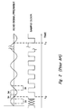
- Figure 2 is a timing diagram showing the desired alignment between the sample clock and the preamble portion of the read signal.
- the preamble is a bit pattern stored at the beginning of every sector (individual sectors not shown) of the disk 16.
- the read channel 10 uses the preamble to calibrate the channel timing with respect to the read signal.
- the read head 18 While reading the preamble, the read head 18 generates a sinusoid (or an approximate sinusoid). The peaks and zero crossings of this preamble sinusoid correspond to the centers of respective data windows 34.
- the centers of the data windows 34 correspond to the data points of the read signal ⁇ the data points are the portions of the read signal that the head 18 generates while positioned directly over the respective storage locations on the surface of the disk 16.
- the timing loop 24 aligns the sample clock with the read signal during the preamble portion and maintains this alignment during the data portion of the read signal.
- a start-up circuit causes the VCO to generate a predetermined edge of the sample clock ⁇ a falling edge in this example ⁇ and thus provides a coarse alignment between the preamble sinusoid and the sample clock.
- the timing loop 24 uses negative feedback to align the rising edges of the sample clock with the sinusoid peaks and to align the falling edges of the sample clock with the sinusoid zero crossings.
- the timing loop 24 provides a fine alignment between the preamble sinusoid and the sample clock. At a predetermined time t 1 , the timing loop 24 is deemed to have aligned sample clock with the preamble sinusoid. To maintain this alignment, however, the loop 24 continues to adjust the VCO frequency as necessary during the remainder of the preamble portion and throughout the data portion of the read signal.
- the timing loop 24 may generate noise that adversely affects other circuits such as those in the read path 14. Specifically, the adjusting of the VCO frequency to acquire and maintain alignment between the sample clock and the read signal often generates significant amounts of noise. Because the timing loop 24 is often integrated on the same die as noise-sensitive circuits, isolation techniques such as using ground plane or shielding are often unavailable, ineffective, prohibitively complex, or prohibitively expensive.
- the timing loop 24 often has a relatively high latency, which often limits the data-read rate of the read channel 10.
- the loop's latency is equivalent to the loop delay, or the time it takes for a signal to travel from an arbitrary starting point in the loop, through the loop, and back to the starting point.
- the phase detector 26 processes a sample of the read signal
- the filtered error signal adjusts the frequency of the sample clock, in response to the phase difference between the sample point of the read signal and the sample clock
- the read circuit 20 generates a subsequent sample in response to the adjusted sample clock, and then the process repeats.
- the timing loop 24 effectively responds more slowly to phase changes between the read signal and sample clock, and thus the loop's margin of stability decreases. If the frequency of the sample clock increases beyond the frequency of the loop 24, then the loop 24 oscillates and causes the read channel 10 to operate improperly. Thus, the relatively high latency of the loop 24 limits the frequency of the sample clock, and thus limits the data-read rate of the read channel 10.
- a conventional digital timing-recovery loop does not suffer from the above-described limitations of the timing loop 24 ( Figure 1).
- a digital timing-recovery loop includes a free-running VCO having a frequency that corresponds to the expected rate at which the read head 18 will read data bits from the disk 16. But instead of adjusting the VCO frequency to acquire and maintain alignment between the sample clock and the read signal, the digital timing-recovery loop adjusts the values of the read samples to the values they would have had if the sample clock and read signal were aligned.
- the digital timing-recovery loop lacks a start-up circuit to provide a coarse alignment between the sample clock and the read signal. Without such a start-up circuit, the digital timing-recovery loop requires a longer time to acquire alignment than the timing loop 24, and thus requires a longer preamble. Because the preamble data pattern is stored at the beginning of each sector of the disk 16, the longer the preamble, the fewer the data bits that the disk 16 can store, and thus the lower the disk's data-storage density.
- a circuit in one aspect of the invention, includes a buffer for receiving and storing two samples of a signal, and a phase calculation circuit for calculating from the samples a phase difference between one of the samples and a predetermined point of the signal.
- Such a circuit can be used to decrease the alignment-acquisition time of a digital timing-recovery loop, and thus allows a shortening of the preamble and a corresponding increase in the data-storage density of a disk.
- the circuit determines an initial phase difference between a disk-drive read signal and a read-signal sample clock.
- the digital timing-recovery loop uses this phase difference to provide an initial coarse alignment between the read signal and the sample clock. By providing an initial coarse alignment, the recovery loop reduces the overall alignment-acquisition time.
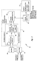
- FIG. 3 is a block diagram of an initial-phase circuit 38 according to an embodiment of the invention.
- the circuit 38 determines an initial phase difference between a disk-drive read signal and a read-signal sample clock.
- a read-sample-interpolator-and-digital-timing-recovery circuit 40 uses this initial phase difference to provide an initial coarse alignment between the read signal and the sample clock. Providing this initial coarse alignment often reduces the overall read-signal/sample-clock alignment-acquisition time, and thus allows one to use a shorter preamble, which allows a corresponding increase in the data-storage density of a storage disk.
- the initial-phase circuit 38 includes a conventional buffer 42 for receiving and storing read-signal samples, a conventional filter 44 for filtering the samples, a phase calculation circuit 46 for calculating the initial phase difference between the read signal and the sample clock, and a phase shifter 48 for adding an anticipated post-sampling phase shift to the initial phase difference.
- the circuit 38 provides this shifted initial phase difference to the circuit 40, which uses this phase difference to obtain an initial coarse alignment between the read signal and the sampling clock.
- the buffer 42, filter 44, and shifter 48 may be omitted such that the circuit 46 receives the read-signal samples directly and provides the initial phase difference directly to the circuit 40.
- the buffer 42 receives and stores first and second raw samples of the read signal from respective sampling analog-to-digital (A/D) converters (not shown).
- the buffer 42 receives eight first raw samples that correspond to eight respective rising edges of the sample clock ( Figures 4 - 10), and receives eight second raw samples that correspond to eight respective falling edges of the sample clock.
- the buffer 42 may receive the first raw samples alternated with the second raw samples ⁇ first raw sample #1, second raw sample #1, first raw sample #2, second raw sample #2 ... ⁇ from a single A/D converter.
- the filter 44 receives the first and second raw samples from the buffer 40 and filters the raw samples to generate a first filtered sample and a second filtered sample. In one embodiment, the filter 44 sets the first filtered sample equal to the average of the first raw samples, and sets the second filtered sample equal to the average of the second raw samples. This averaging typically eliminates most or all of the noise superimposed on the read signal.
- the phase-calculation circuit 46 includes a function circuit 52 for calculating a value that represents the relative phase difference ⁇ ', or the absolute phase difference ⁇ between the read signal and the sample clock, an inverse function circuit 54 for calculating ⁇ ' or ⁇ from the calculated value, and an optional phase interpolator 56 for calculating ⁇ in embodiments where the circuits 52 and 54 calculate only ⁇ '.
- the circuit 46 calculates ⁇ equal to the absolute phase lead of a sample-clock rising edge ⁇ which in these embodiments corresponds to the first filtered sample as discussed above ⁇ with respect to the immediately succeeding peak of the preamble sinusoid.
- the function circuit 52 calculates the tangent of the absolute phase lead ⁇ equal to the ratio of the first filtered sample to the second filtered sample.
- the circuit 54 includes a look-up memory 58, which provides ⁇ equal to the arctangent of this ratio. Therefore, in this embodiment, the phase interpolator 56 is omitted.
- the circuit 46 takes advantage of the range of the tangent magnitudes, and thus the range of the corresponding arctangent values, being the same for each quadrant of the preamble sinusoid.
- the size of the look-up memory 58 is half that of the memory 58 in the first embodiment, and the arctangent value provided by the memory 58, i.e., the relative phase lead ⁇ ', is the phase lead of the first filtered sample within the quadrant of the preamble sinusoid with which the sample coincides.
- the interpolator 56 identifies this quadrant by examining the polarities of the first and second filtered samples. The interpolator 56 then combines this quadrant information with ⁇ ' to calculate ⁇ .
- the circuit 46 takes advantage of the range of the tangent magnitudes from 0 to 1, and thus the range of corresponding arctangent values, being the same for each half quadrant of the preamble sinusoid. Consequently, the look-up memory 58 need only store half a quadrant's worth of arctangent values.
- the size of the memory 58 is half the size of the memory 58 in the second embodiment of the circuit 46 and one quarter the size of the memory 58 in the first embodiment.
- the function circuit 52 determines the ratio of the minimum of the first and second samples to the maximum of the first and second samples. This insures that the ratio, and thus the tangent of ⁇ ', is always between 0 and 1.
- the arctangent value ⁇ ' provided by the memory 58 is the relative phase of the first filtered sample within the half quadrant of the preamble sinusoid with which the sample coincides.
- the interpolator 56 identifies this half quadrant by examining the polarities of the first and second filtered samples. The interpolator 56 then combines with ⁇ ' to calculate ⁇ .
- the phase shifter 48 adds to ⁇ any phase shift that the read signal experiences between the sampling A/Ds (not shown) and the read-sample interpolation portion of the circuit 40. This allows the interpolation portion of the circuit 40 to accurately interpolate the values of the read signal at the data points.
- a finite-impulse-response (FIR) filter ( Figure 16) may process the read-signal samples before the interpolation portion of the circuit 40 interpolates them. Therefore, the shifter 48 is programmed with the expected phase shift (lead or lag) that the FIR will impart to the read signal. Because the interpolation portion of the circuit 40 requires the total phase between the sample clock and read signal at the point of interpolation, the shifter 48 adjusts ⁇ such that ⁇ reflects the phase shift of the FIR filter.
- the operation of the initial-phase circuit 38 is discussed below in conjunction with Figures 3 - 13, and a specific example is discussed below in conjunction with Figures 3, 7, 12, and 13. For example purposes, this operation is discussed where the circuit 38 incorporates the third embodiment (discussed above) of the phase-calculation circuit 46, it being understood that the circuit 38 operates in a similar manner where it incorporates the first or second embodiments of the circuit 46.
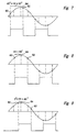
- Figures 4 - 10 respectively illustrate seven possible alignments between the preamble sinusoid of the read signal and the sample clock, and thus illustrate seven possible regions of the absolute phase ⁇ .
- the preamble sinusoid is shown as noiseless such that first samples 60 and second samples 62 respectively equal the first and second filtered samples from the filter 44 ( Figure 3). More specifically, Figures 4 - 10 illustrate seven possible positions that the rising edges of the sample clock, and thus the first samples 60, can have with respect to the peaks 64 of the sinusoid.
- the alignment convention is that the rising edges, and thus the first samples 60, lead the immediately following peaks 64 by a phase angle 0° ⁇ ⁇ 180°, where values of ⁇ are given with respect to the period of the preamble sinusoid.
- other alignment conventions can be used, such as where values of ⁇ are given with respect to the sampling period, which here is one fourth the period of the preamble sinusoid.
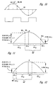
- Figures 11 - 12 illustrate how the phase calculation circuit 46 (Figure 3) can use a tangent function to obtain the phase angle between the preamble sinusoid and the sample clock.
- Figure 11 is a phase diagram showing the positive half of the preamble sinusoid of Figure 9.
- the first sample 60 1 which corresponds to a rising edge of the sample clock, leads the sinusoid peak 64 by the phase angle ⁇ 1 .
- Figure 12 is a phase diagram of the positive half of the preamble sinusoid of Figure 7.
- Tan ⁇ (0° ⁇ 45°) 1/Tan(90°- ⁇ ) (90° ⁇ (90°- ⁇ ) ⁇ 45°).
- the look-up memory 58 stores values of arctana over only a half quadrant (0° - 45°). This allows the look-up memory 58 to be 1 ⁇ 4 the size needed for the first embodiment and 1 ⁇ 2 the size needed for the second embodiment.
- ⁇ ' is the relative phase angle of the first sample 60 within the half-quadrant of the preamble sinusoid in which the first sample lies.
- ⁇ ' indicates the location of the first sample 60 within the half quadrant 66 (45° - 90°).
- Figure 13 is a 7-bit word 70 of the phase angle ⁇ according to an embodiment of the invention.
- the bits A0 - A4 are derived from arctan ⁇ ', and thus indicate the relative phase of the first sample 60 ( Figures 11 and 12) within a half quadrant. Therefore, the resolution of the byte 70 is 45° ⁇ 2 5 ⁇ 1.41°.
- A5 indicates whether ⁇ is greater than or less than 45°.
- A6 indicates whether ⁇ is greater than or less than 90°.
- the circuit 54 retrieves the corresponding value for Arctan ⁇ ', which approximately equals 2.81°, from the look-up memory 58.
- the circuit 56 then calculates an intermediate binary value X and bit A6 according to the following equation.
- the values of the first and second samples 60 2 and 62 2 ( Figure 12) are respectively represented by FS and SS.
- X - X6 0111111
- the shifter 48 adds any post-sampling phase shift to ⁇ to obtain the total phase shift between the sample clock and the preamble sinusoid as seen by the sample interpolator portion of the circuit 40.
- an FIR filter ( Figure 16) in the read path may add to or subtract from the phase lead ⁇ generated by the initial-phase circuit 46. Because this post-sampling phase shift may cause A6:A0 to "wrap around", A6:A0 is altered as described below.
- wrap around refers to the post-sampling phase shift causing ⁇ to cross a 90° boundary. That is, if ⁇ 90°, the post-sampling phase shift wraps around the total phase lead ⁇ to greater than 90°, and if ⁇ > 90°, the post-sampling phase shift wraps around ⁇ to less than 90°.
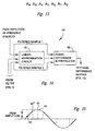
- Figure 14 is a block diagram of a fourth embodiment of the phase-calculation circuit 46 of Figure 3.
- This embodiment generates the relative half-quadrant phase ⁇ ' by approximating a portion of the preamble sinusoid as linear and then successively approximating ⁇ '.
- this embodiment needs more time to calculate ⁇ ' and depends on the sampled peak amplitude of the preamble sinusoid. But it does not require the look-up memory 58 ( Figure 3), and thus occupies less die layout area than the first, second, and third embodiments.
- the fourth embodiment of the circuit 46 includes a linear-approximation circuit 70, which replaces the function and inverse function circuits 52 and 54 of Figure 3, and includes the phase-interpolator 56.
- the circuit 70 calculates ⁇ ' from the first and second filtered samples and from the sampled peak amplitude of the preamble sinusoid.
- a circuit for calculating and providing the sampled peak amplitude is discussed in U.S. Patent App. entitled “A Circuit And Method For Controlling The Gain Of An Amplifier Based On The Sum Of Samples Of The Amplified Signal", Pat. App. Serial No. , Attorney Docket No. 99-S-165 (1678-17) which has the same filing date as the present application, and U.S. Patent App. entitled “A Circuit And Method For Controlling The Gain Of An Amplifier", Pat. App. Serial No. , Attorney Docket No. 99-S-188 (1678-19) which has the same filing date as the present application and incorporated by reference.
- Figure 15 shows the preamble sinusoid of Figure 7 superimposed on linear approximations of the following half-quadrants of the preamble sinusoid: 0° - 45°, 135° - 225°, and 315° - 360°. These half-quadrants are chosen because they are more linear than the other half-quadrants of the preamble sinusoid. By linearizing these half-quadrants, the circuit 46 can calculate ⁇ ' within a half quadrant as proportional to the sample lying within that half quadrant as discussed below. Referring to Figures 14 and 15, the operation of the circuit 46 is discussed by way of example.
- phase lead ⁇ of the first sample 60 is 87.18° with respect to the peak 64
- the first sample 60 0.049
- the peak amplitude 1
- ⁇ ' has a resolution of 5 bits B4:B0.
- the phase of the linearly approximated half quadrant ranges from 0° - 45°
- a 1 for B3 represents 0.176, which is the linear halfway point between 0 and 0.353
- a 1 for B2 represents 0.088, which is the linear halfway point between 0 and 0.176
- a 1 for B1 represents 0.044, which is the linear halfway point between 0 and 0.088
- a 1 for B0 represents 0.022, which is the linear halfway point between 0 and .044.
- the linear-approximation circuit 70 uses these values to successively approximate ⁇ ' in five steps, one step for each bit B4:B0.
- the linear-approximation circuit 70 determines which of the first and second filtered samples lies within one of the linearly approximated half quadrants. Therefore, in this example, the circuit 70 determines that the first sample 60 lies within such a half quadrant.
- the circuit 70 uses the first sample 60 to successively approximate ⁇ '.
- the circuit 70 compares the sample to 0.353 to generate B4.
- the circuit 70 compares the sample to 0.176 to generate B3.
- the circuit 70 compares the sample to 0.088 to generate B2.
- the circuit 70 compares the sample to 0.044 to generate B1.
- B4:B0 00010, which is the same as calculated by the inverse-function circuit 54 of Figure 3 in the above example for the same value, 0.049, of the first sample.
- the interpolator 56 then calculates ⁇ from B4:B0 and the values of the first and second samples 60 and 62 in the manner described above in conjunction with Figures 3 - 13.
- Figure 16 is a block diagram of a digital-baud-rate-timing-recovery circuit 80 according to an embodiment of the invention.
- the circuit 80 incorporates the initial-phase circuit 38 and the sample interpolator and timing recovery loop 40 of Figure 3.
- the circuit 38 may include any of the embodiments of the phase-calculation circuit 46 of Figures 3 and 14. Although details of the circuit 80 are discussed below, further details are disclosed in U.S. Patent Application Ser. No. 09/387,146, "Digital Timing Recovery Using Baud Rate Sampling", filed August 31, 1999 and incorporated by reference.
- the first and second samples are input to an finite-impulse-response (FIR) filter 82, which equalizes each sample to its nearest expected signal level, and then provides the equalized first and second samples on data paths 84 and 85, respectively.
- FIR finite-impulse-response
- a sample interpolator 86 operates on the incoming equalized samples and provides interpolated samples calculated at an interpolation interval provided by an accumulator 88.
- the sample interpolator 86 has three output paths. Two of the output paths provide the two interpolated samples S1 and S2, which are derived in parallel by the interpolator 86.
- the third output path provides an un-interpolated sample S3 as may be necessary in an undersampling condition.
- the interpolator 86 provides all three samples S1, S2, and S3 to an elastic buffer 90 and to a mini-elastic buffer 92, which provides the correct stream of data to a phase detector 94 (described below). Note that because of the parallel sampling paths throughout the system, the interpolator 86 outputs two interpolated samples S1 and S2 during each cycle of normal operation. During an oversample condition, the interpolator 86 provides one valid interpolated sample and one bogus interpolated sample.
- the interpolator 86 outputs three samples: the interpolated sample S1, the interpolated sample S2, and the uninterpolated sample S3, which is provided by the interpolator 86 to compensate for the fact that the interpolator 86 cannot interpolate two samples in one (half-rate) cycle.
- the interpolator 86 also provides the interpolated samples S1 and S2 to the phase detector 94, which determines the phase difference between the interpolated samples S1 and S2 and the expected values of the samples S1 and S2, and which generates a corresponding phase-error signal.
- the phase detector 94 provides this phase-error signal to a proportional-integral filter 96, which provides the filtered error signal to the accumulator 88.
- the accumulator 88 derives the fractional delay, also known as the interpolation value tau ( ⁇ ), from the filtered error signal.
- the interpolation value T is used to select a set of coefficients employed by the sample interpolator 86 to derive the interpolation samples S1 and S2. These coefficient values are stored in a read only memory (ROM) 98, which receives the ⁇ value from the accumulator 88 and provides to the sample interpolator 86 the appropriate coefficient values corresponding to the desired interpolation interval.
- ROM read only memory
- the initial phase circuit 38 calculates a gain-independent initial phase ⁇ representing the phase lead of the sample clock with respect to the preamble sinusoid.
- the circuit 38 provides the bits A5:A0 of ⁇ to the accumulator 88 and to the ROM 98. This portion of ⁇ is used to select the initial value that is input to the sample interpolator 86 at the start of a read cycle.
- the circuit 38 provides the bit A6 of ⁇ to the elastic buffer 90 and to the phase detector 94.
- Figure 17 is a block diagram of a disk-drive system 100, which includes a disk drive 102, according to an embodiment of the invention.
- the disk drive 102 includes a read channel 103, which incorporates the recovery circuit 80 of Figure 16.
- the disk drive 102 includes a combination write/read head 104, a write-channel circuit 106 for generating and driving the head 104 with a write signal, and a write controller 108 for interfacing the write data to the write-channel circuit 106.
- the disk drive 102 also includes the read channel 103 for receiving a read signal from the head 104 and for recovering data from the read signal, and includes a read controller 114 for organizing the read data.
- the disk drive 102 further includes a storage medium such as one or more disks 116, each of which may store data on one or both sides.
- the read/write head 104 writes/reads the data stored on the disks 116 and is connected to a movable support arm 118.
- a position system 120 provides a control signal to a voice-coil motor (VCM) 122, which positionally maintains/moves the arm 118 so as to positionally maintain/radially move the head 104 over the desired data on the respective disks 116.
- VCM voice-coil motor
- a spindle motor (SPM) 124 and a SPM control circuit 126 respectively rotate the disks 116 and maintain them at the proper rotational speed.
- the disk-drive system 100 also includes write and read interface adapters 128 and 130 for respectively interfacing the write and read controllers 108 and 114 to a system bus 132, which is specific to the system used.
- Typical system busses include ISA, PCI, S-Bus, Nu-Bus, etc.
- the system 10 also typically has other devices, such as a random access memory (RAM) 134 and a central processing unit (CPU) 136 coupled to the bus 132.
- RAM random access memory
- CPU central processing unit
Landscapes
- Engineering & Computer Science (AREA)
- Signal Processing (AREA)
- Synchronisation In Digital Transmission Systems (AREA)
- Signal Processing For Digital Recording And Reproducing (AREA)
Abstract
Description

Claims (26)
- A circuit, comprising:a buffer operable to receive and store two samples of a signal; anda phase calculation circuit coupled to the buffer and operable to calculate from the samples a phase difference between one of the samples and a predetermined point of the signal.
- The circuit of claim 1, further comprising a filter coupled to the buffer and to the phase calculation circuit and operable to receive the stored samples from the buffer, filter the samples, and provide the filtered samples to the phase calculator.
- The circuit of claim 1, further comprising a phase shifter coupled to the phase calculation circuit and operable to shift the calculated phase difference by an amount equal or approximately equal to a post-sampling phase shift applied to the signal.
- A circuit, comprising:a buffer operable to receive and store two samples of a signal;a function circuit coupled to the buffer and operable to calculate from the samples a trigonometric value of a phase difference between one of the samples and a predetermined point of the signal; andan inverse-function circuit coupled to the function circuit and operable to calculate the phase difference from the trigonometric value.
- A circuit, comprising:a filter operable to generate first and second filtered samples of a periodic signal;a function circuit coupled to the filter and operable to calculate a trigonometric value corresponding to the location of one of the filtered samples with respect to a predetermined point of the signal, the trigonometric value being equal to a ratio of the filtered samples;an inverse-function circuit coupled to the function circuit and operable to calculate a component of the sample location from the trigonometric value; andan interpolator coupled to the inverse-function circuit and the filter and operable to determine the sample location from the component and the filtered samples.
- The circuit of claim 5 wherein the filter is operable to:generate the first filtered sample equal to an average of first samples that are spaced apart from each other by or approximately by half a period of the signal; andgenerate the second filtered sample equal to an average of second samples that are spaced apart from each other by or approximately by half a period of the signal and that are respectively spaced apart from the first samples by or approximately by a quarter period of the signal.
- The circuit of claim 5 wherein:if the absolute value of one of the filtered samples is larger than the absolute value of the other filtered sample, then the function circuit is operable to calculate the trigonometric value equal to the tangent of the smaller absolute value divided by the larger absolute value; andif the absolute values of the filtered samples are equal, then the function circuit is operable to calculate the trigonometric value equal to the tangent of 45°.
- The circuit of claim 5 wherein:the inverse-function circuit comprises a memory operable to store values of the first component of the sample location; andwherein the inverse-function circuit is operable to calculate the component of the sample location equal to a stored value that corresponds to the trigonometric value.
- The circuit of claim 5 wherein:the inverse-function circuit is operable to calculate the component of the sample location equal to or approximately equal to the location of the sample within a half quadrant of the signal; andthe interpolator is operable to calculate the location of the half quadrant of the signal within which the sample lies.
- A data read channel, comprising:a sampler operable to sample a read signal at first and second preamble times during a preamble portion and at a first data time during a data portion, and operable to generate corresponding preamble-sample values and a corresponding data-sample value;a sample interpolator coupled to the sampler, operable to receive a phase difference between the first data time and a second data time that corresponds to a data window of the read signal, and operable to generate from the data-sample value and the phase difference an adjusted sample value that equals or approximately equals the value of the read signal at the second time;a tracking circuit coupled to the sample interpolator and operable to track and update the phase difference; andan initial-phase circuit coupled to the sampler, sample interpolator, and tracking circuit and operable to calculate an initial value of the phase difference from the first and second preamble values.
- The data read circuit of claim 10 wherein:the data window has a center; andthe second data time corresponds to the center of the data window.
- A disk-drive system, comprising:a data-storage disk having a surface and operable to store a preamble and data values;a motor coupled to and operable to rotate the disk;a read head operable to generate a read signal that includes the preamble followed by a data portion that includes the data values, each of the data values located within a respective data window of the read signal, each of the data windows having a center;a read-head positioning assembly operable to move the read head over the surface of the disk; anda read channel, comprisinga sampler operable to sample the preamble of the read signal at first and second preamble times and the data portion at a first data time and to generate corresponding preamble-sample values and a corresponding data-sample value,a sample interpolator coupled to the sampler, operable to receive a phase difference between the first data time and a second data time corresponding to the center of a data window, and operable to generate from the data-sample value and the phase difference an adjusted sample value that equals or approximately equals the value of the read signal at the center of the data window,a tracking circuit coupled to the sample interpolator and operable to track and update the phase difference, andan initial-phase circuit coupled to the sampler, sample interpolator, and tracking circuit and operable to calculate an initial value of the phase difference from the first and second preamble values.
- A method, comprising:generating two samples of a signal; anddetermining from the samples a phase difference between one of the samples and a predetermined point of the signal.
- The method of claim 13 further comprising filtering noise from the samples before the determining.
- The method of claim 13 further comprising shifting the determined phase difference by an amount equal or approximately equal to a predetermined post-sampling phase shift experienced by the signal.
- A method, comprising:generating two samples of a signal;determining from the samples a trigonometric value of a phase difference between one of the samples and a predetermined point of the signal; andcalculating the phase difference from the trigonometric value.
- The method of claim 16 wherein:the trigonometric value comprises a tangent value; andthe determining comprises setting the tangent value equal to a quotient of the two samples.
- The method of claim 16 wherein:the trigonometric value comprises a tangent value; andthe determining comprises setting the tangent value equal to a quotient of the two samples, the quotient being less than or equal to 1.
- The method of claim 16 wherein:the trigonometric value comprises a tangent value;the determining comprises setting the tangent value equal to the quotient of the two samples; andthe calculating comprises setting the phase difference equal to the arctangent of the tangent value.
- The method of claim 16 wherein:the trigonometric value comprises a tangent value;the determining comprises setting the tangent value equal to the quotient of the two samples, the quotient being less than or equal to one; andthe calculating comprises setting the phase difference equal to the arctangent of the tangent value.
- A method, comprising:generating first and second samples of a periodic signal;calculating a trigonometric value corresponding to the location of one of the samples with respect to a predetermined point of the signal, the trigonometric value being equal to a ratio of the samples;calculating a relative phase of the sample location from the trigonometric value; anddetermining the sample location from the relative phase and the filtered samples.
- The method of claim 21 wherein the generating comprises:generating first raw samples that are spaced apart from each other by or approximately by half a period of the signal;averaging the first raw samples to generate the first sample;generating second raw samples that are spaced apart from each other by or approximately by half a period of the signal and that are respectively spaced apart from the first raw samples by or approximately by a quarter period of the signal; andaveraging the second raw samples to generate the second sample.
- The method of claim 21 wherein the calculating the trigonometric value comprises:if the absolute value of one of the samples is larger than the absolute value of the other filtered sample, then setting the trigonometric value equal to the tangent of the quotient of the smaller absolute value to the larger absolute value; andif the absolute values of the are equal, then setting the trigonometric value equal one.
- The method of claim 21 wherein the calculating the relative phase comprises retrieving from a look-up table the relative phase of the sample location that corresponds to the trigonometric value.
- The method of claim 21 wherein:the calculating the relative phase comprises calculating the fine position of the sample location; andthe determining comprises determining a coarse position of the sample location.
- The method of claim 21 wherein:the periodic signal comprises a sinusoid;the predetermined point of the signal comprises a peak of the sinusoid;the sample location comprises the location of the first sample;the first sample leads the predetermined point;the calculating the relative phase comprises setting the relative phase of the sample location equal to the phase difference between the sample location and a boundary of a half quadrant of the periodic signal within which the sample lies; andthe determining comprises setting the phase difference between the sample location and the predetermined point equal to,90° minus the relative phase of the sample location if the first and second samples have the same polarities and the absolute value of the first sample is less than the absolute value of the second sample,45° if the first sample equals the second sample,the relative phase of the sample location if the first and second samples have the same polarities and the absolute value of the first sample is greater than the absolute value of the second sample,180° minus the relative phase of the sample location if the first and second samples have opposite polarities and the absolute value of the first sample is greater than the absolute value of the second sample,135° if the first and the second samples have opposite polarities and equal absolute values, and90° plus the relative phase of the sample location if the first and second samples have opposite signs and the absolute value of the first sample is less than the absolute value of the second sample.
Applications Claiming Priority (2)
| Application Number | Priority Date | Filing Date | Title |
|---|---|---|---|
| US503453 | 1995-07-17 | ||
| US09/503,453 US6775084B1 (en) | 2000-02-14 | 2000-02-14 | Circuit and method for determining the phase difference between a sample clock and a sampled signal |
Publications (3)
| Publication Number | Publication Date |
|---|---|
| EP1126616A2 true EP1126616A2 (en) | 2001-08-22 |
| EP1126616A3 EP1126616A3 (en) | 2003-11-12 |
| EP1126616B1 EP1126616B1 (en) | 2006-08-23 |
Family
ID=24002150
Family Applications (1)
| Application Number | Title | Priority Date | Filing Date |
|---|---|---|---|
| EP01300785A Expired - Lifetime EP1126616B1 (en) | 2000-02-14 | 2001-01-30 | Circuit and method for determining the phase difference between a sample clock and a sampled signal |
Country Status (4)
| Country | Link |
|---|---|
| US (1) | US6775084B1 (en) |
| EP (1) | EP1126616B1 (en) |
| JP (1) | JP2001273720A (en) |
| DE (1) | DE60122402D1 (en) |
Families Citing this family (18)
| Publication number | Priority date | Publication date | Assignee | Title |
|---|---|---|---|---|
| US7830630B2 (en) | 2001-06-28 | 2010-11-09 | Stmicroelectronics, Inc. | Circuit and method for detecting the phase of a servo signal |
| US7839594B2 (en) * | 2001-06-28 | 2010-11-23 | Stmicroelectronics, Inc. | Data-storage disk having few or no spin-up wedges and method for writing servo wedges onto the disk |
| US7082005B2 (en) * | 2001-10-24 | 2006-07-25 | Agere Systems Inc. | Servo data detection in the presence or absence of radial incoherence using digital interpolators |
| US7190754B1 (en) * | 2001-12-24 | 2007-03-13 | Rambus Inc. | Transceiver with selectable data rate |
| US20030123174A1 (en) * | 2001-12-28 | 2003-07-03 | Mark Hennecken | Continuously variable storage device data transfer rate |
| US7793020B1 (en) * | 2002-11-27 | 2010-09-07 | International Business Machines Corporation | Apparatus and method to read information from an information storage medium |
| US7602863B2 (en) * | 2004-09-24 | 2009-10-13 | Seagate Technology Llc | Method and apparatus for providing iterative timing recovery |
| US7773324B2 (en) * | 2005-04-12 | 2010-08-10 | Stmicroelectronics, Inc. | Phase acquisition loop for a read channel and related read channel, system, and method |
| US7768732B2 (en) * | 2005-04-12 | 2010-08-03 | Stmicroelectronics, Inc. | Gain controller for a gain loop of a read channel and related gain loops, read channels, systems, and methods |
| US7675702B2 (en) * | 2006-05-24 | 2010-03-09 | Seagate Technology Llc | Reduced convolution for repetitive disturbance rejection |
| US7764759B2 (en) * | 2006-06-13 | 2010-07-27 | Gennum Corporation | Linear sample and hold phase detector for clocking circuits |
| US7974035B2 (en) * | 2006-06-29 | 2011-07-05 | Broadcom Corporation | Timing recovery optimization using disk clock |
| US7869547B1 (en) * | 2007-02-15 | 2011-01-11 | Link—A—Media Devices Corporation | Preamble acquisition without second order timing loops |
| US8036312B2 (en) * | 2007-03-30 | 2011-10-11 | Freescale Semiconductor, Inc. | System and method for determining signal phase |
| US7995304B2 (en) * | 2009-05-27 | 2011-08-09 | Seagate Technology Llc | Circuits that use a postamble signal to determine phase and frequency errors in the acquisition of a preamble signal |
| WO2011119802A2 (en) * | 2010-03-26 | 2011-09-29 | Shell Oil Company | Seismic clock timing correction using ocean acoustic waves |
| US8049982B1 (en) | 2010-07-30 | 2011-11-01 | Lsi Corporation | Methods and apparatus for measuring servo address mark distance in a read channel using selective fine phase estimate |
| US8780470B1 (en) | 2013-03-11 | 2014-07-15 | Western Digital Technologies, Inc. | Disk drive adjusting digital phase locked loop over sector data with frequency induced phase error measured over preamble |
Family Cites Families (12)
| Publication number | Priority date | Publication date | Assignee | Title |
|---|---|---|---|---|
| US3956623A (en) * | 1974-10-21 | 1976-05-11 | Gte Automatic Electric Laboratories Incorporated | Digital phase detector |
| US4412339A (en) | 1981-09-24 | 1983-10-25 | Advanced Micro Devices, Inc. | Zero-crossing interpolator to reduce isochronous distortion in a digital FSK modem |
| IT1155558B (en) * | 1982-07-19 | 1987-01-28 | Cselt Centro Studi Lab Telecom | PROCEDURE AND INSTRUMENT FOR MEASURING THE AMPLITUDE OF A PERIODIC SIGNAL STRONGLY AFFECTED BY NOISE AND WITHOUT PHASE REFERENCE |
| JP2589759B2 (en) | 1988-05-27 | 1997-03-12 | 松下電器産業株式会社 | Data identification device |
| US5359631A (en) | 1992-09-30 | 1994-10-25 | Cirrus Logic, Inc. | Timing recovery circuit for synchronous waveform sampling |
| US5486867A (en) | 1993-11-30 | 1996-01-23 | Raytheon Company | High resolution digital phase detector |
| JP3077881B2 (en) * | 1995-03-07 | 2000-08-21 | 日本電気株式会社 | Demodulation method and demodulation device |
| US5848099A (en) | 1996-05-30 | 1998-12-08 | Qualcomm Incorporation | Method and system for testing phase imbalance in QPSK receivers |
| US5835295A (en) * | 1996-11-18 | 1998-11-10 | Cirrus Logice, Inc. | Zero phase restart interpolated timing recovery in a sampled amplitude read channel |
| US6529460B1 (en) | 1998-01-31 | 2003-03-04 | Seagate Technology Llc | Detection of pulse peak instance and amplitude in a storage drive |
| US6307696B1 (en) * | 1999-05-06 | 2001-10-23 | Maxtor Corporation | Digital zero-phase restart circuit |
| US6493403B1 (en) * | 2000-02-02 | 2002-12-10 | Infineon Technologies North America Corp. | Asynchronous timing for interpolated timing recovery |
-
2000
- 2000-02-14 US US09/503,453 patent/US6775084B1/en not_active Expired - Fee Related
-
2001
- 2001-01-30 EP EP01300785A patent/EP1126616B1/en not_active Expired - Lifetime
- 2001-01-30 DE DE60122402T patent/DE60122402D1/en not_active Expired - Lifetime
- 2001-02-14 JP JP2001037421A patent/JP2001273720A/en active Pending
Also Published As
| Publication number | Publication date |
|---|---|
| US6775084B1 (en) | 2004-08-10 |
| EP1126616A3 (en) | 2003-11-12 |
| EP1126616B1 (en) | 2006-08-23 |
| JP2001273720A (en) | 2001-10-05 |
| DE60122402D1 (en) | 2006-10-05 |
Similar Documents
| Publication | Publication Date | Title |
|---|---|---|
| US6366225B1 (en) | Circuit and method for determining the phase difference between a sample clock and a sample signal by linear approximation | |
| US6775084B1 (en) | Circuit and method for determining the phase difference between a sample clock and a sampled signal | |
| US6487672B1 (en) | Digital timing recovery using baud rate sampling | |
| US6738205B1 (en) | Self-writing of servo patterns in disk drives | |
| US5917668A (en) | Synchronous read channel employing a frequency synthesizer for locking a timing recovery phase-lock loop to a reference frequency | |
| US7180693B2 (en) | Method and apparatus for maximum likelihood detection of data employing interpolation with compensation of signal asymmetry | |
| US6369661B1 (en) | Phase interpolation circuits and methods and systems using the same | |
| US7298576B2 (en) | Magnetic recording medium and magnetic recording/reproducing apparatus | |
| US8837068B1 (en) | Two dimensional magnetic recording servo system adaptive combination | |
| US5442492A (en) | Data recovery procedure using DC offset and gain control for timing loop compensation for partial-response data detection | |
| CN101968968A (en) | Systems and methods for two tier sampling correction in a data processing circuit | |
| JPH07169033A (en) | Disk drive | |
| US10068609B1 (en) | Variable frequency write pattern generation | |
| JP4480191B2 (en) | Phase locked loop system | |
| US6867941B1 (en) | Circuit and method for controlling the gain of an amplifier based on the sum of samples of the amplified signal | |
| US6157604A (en) | Sampled amplitude read channel employing a baud rate estimator for digital timing recovery in an optical disk storage device | |
| EP1111606B1 (en) | Clock adjustment apparatus for a data reproduction system and an apparatus having a data reproduction system including such a clock adjustment apparatus | |
| US7433286B2 (en) | Jitter detection apparatus | |
| US6636120B2 (en) | Decimated digital phase-locked loop for high-speed implementation | |
| EP1713069A1 (en) | A phase acquisition loop for a read channel and related read channel, system, and method | |
| US7345839B2 (en) | Signal processing in a disc drive | |
| US6778345B1 (en) | Circuit and method for controlling the gain of an amplifier | |
| JP4098660B2 (en) | Disk storage device and sync mark detection method | |
| US9171571B2 (en) | Read channel operable to calibrate a coefficient of a filter, such as an FIR filter, disposed before an interpolated-timing-recovery circuit, and related integrated circuit, system, and method | |
| US7697224B2 (en) | Storing AD sampled data of read/write channel into ECC SRAM |
Legal Events
| Date | Code | Title | Description |
|---|---|---|---|
| PUAI | Public reference made under article 153(3) epc to a published international application that has entered the european phase |
Free format text: ORIGINAL CODE: 0009012 |
|
| AK | Designated contracting states |
Kind code of ref document: A2 Designated state(s): AT BE CH CY DE DK ES FI FR GB GR IE IT LI LU MC NL PT SE TR |
|
| AX | Request for extension of the european patent |
Free format text: AL;LT;LV;MK;RO;SI |
|
| PUAL | Search report despatched |
Free format text: ORIGINAL CODE: 0009013 |
|
| AK | Designated contracting states |
Kind code of ref document: A3 Designated state(s): AT BE CH CY DE DK ES FI FR GB GR IE IT LI LU MC NL PT SE TR |
|
| AX | Request for extension of the european patent |
Extension state: AL LT LV MK RO SI |
|
| 17P | Request for examination filed |
Effective date: 20040511 |
|
| AKX | Designation fees paid |
Designated state(s): DE FR GB IT |
|
| 17Q | First examination report despatched |
Effective date: 20050224 |
|
| GRAP | Despatch of communication of intention to grant a patent |
Free format text: ORIGINAL CODE: EPIDOSNIGR1 |
|
| GRAS | Grant fee paid |
Free format text: ORIGINAL CODE: EPIDOSNIGR3 |
|
| GRAA | (expected) grant |
Free format text: ORIGINAL CODE: 0009210 |
|
| AK | Designated contracting states |
Kind code of ref document: B1 Designated state(s): DE FR GB IT |
|
| PG25 | Lapsed in a contracting state [announced via postgrant information from national office to epo] |
Ref country code: IT Free format text: LAPSE BECAUSE OF FAILURE TO SUBMIT A TRANSLATION OF THE DESCRIPTION OR TO PAY THE FEE WITHIN THE PRESCRIBED TIME-LIMIT;WARNING: LAPSES OF ITALIAN PATENTS WITH EFFECTIVE DATE BEFORE 2007 MAY HAVE OCCURRED AT ANY TIME BEFORE 2007. THE CORRECT EFFECTIVE DATE MAY BE DIFFERENT FROM THE ONE RECORDED. Effective date: 20060823 |
|
| REG | Reference to a national code |
Ref country code: GB Ref legal event code: FG4D |
|
| REF | Corresponds to: |
Ref document number: 60122402 Country of ref document: DE Date of ref document: 20061005 Kind code of ref document: P |
|
| PG25 | Lapsed in a contracting state [announced via postgrant information from national office to epo] |
Ref country code: DE Free format text: LAPSE BECAUSE OF FAILURE TO SUBMIT A TRANSLATION OF THE DESCRIPTION OR TO PAY THE FEE WITHIN THE PRESCRIBED TIME-LIMIT Effective date: 20061124 |
|
| PGFP | Annual fee paid to national office [announced via postgrant information from national office to epo] |
Ref country code: GB Payment date: 20070124 Year of fee payment: 7 |
|
| ET | Fr: translation filed | ||
| PLBE | No opposition filed within time limit |
Free format text: ORIGINAL CODE: 0009261 |
|
| STAA | Information on the status of an ep patent application or granted ep patent |
Free format text: STATUS: NO OPPOSITION FILED WITHIN TIME LIMIT |
|
| 26N | No opposition filed |
Effective date: 20070524 |
|
| PGFP | Annual fee paid to national office [announced via postgrant information from national office to epo] |
Ref country code: FR Payment date: 20070109 Year of fee payment: 7 |
|
| GBPC | Gb: european patent ceased through non-payment of renewal fee |
Effective date: 20080130 |
|
| REG | Reference to a national code |
Ref country code: FR Ref legal event code: ST Effective date: 20081029 |
|
| PG25 | Lapsed in a contracting state [announced via postgrant information from national office to epo] |
Ref country code: GB Free format text: LAPSE BECAUSE OF NON-PAYMENT OF DUE FEES Effective date: 20080130 |
|
| PG25 | Lapsed in a contracting state [announced via postgrant information from national office to epo] |
Ref country code: FR Free format text: LAPSE BECAUSE OF NON-PAYMENT OF DUE FEES Effective date: 20080131 |