EP1126596A1 - Feedforward amplifier - Google Patents
Feedforward amplifier Download PDFInfo
- Publication number
- EP1126596A1 EP1126596A1 EP00915351A EP00915351A EP1126596A1 EP 1126596 A1 EP1126596 A1 EP 1126596A1 EP 00915351 A EP00915351 A EP 00915351A EP 00915351 A EP00915351 A EP 00915351A EP 1126596 A1 EP1126596 A1 EP 1126596A1
- Authority
- EP
- European Patent Office
- Prior art keywords
- signal
- output
- distortion
- splitter
- component
- Prior art date
- Legal status (The legal status is an assumption and is not a legal conclusion. Google has not performed a legal analysis and makes no representation as to the accuracy of the status listed.)
- Withdrawn
Links
Images



Classifications
-
- H—ELECTRICITY
- H03—ELECTRONIC CIRCUITRY
- H03F—AMPLIFIERS
- H03F1/00—Details of amplifiers with only discharge tubes, only semiconductor devices or only unspecified devices as amplifying elements
- H03F1/32—Modifications of amplifiers to reduce non-linear distortion
- H03F1/3223—Modifications of amplifiers to reduce non-linear distortion using feed-forward
- H03F1/3229—Modifications of amplifiers to reduce non-linear distortion using feed-forward using a loop for error extraction and another loop for error subtraction
-
- H—ELECTRICITY
- H03—ELECTRONIC CIRCUITRY
- H03F—AMPLIFIERS
- H03F2200/00—Indexing scheme relating to amplifiers
- H03F2200/451—Indexing scheme relating to amplifiers the amplifier being a radio frequency amplifier
Definitions
- the present invention relates to a feedforward amplifier for carrying out low distortion amplification in a radio frequency band.
- a feedforward amplifier that achieves a low distortion characteristic by feedforward distortion compensation is often used as an amplifier for carrying out low distortion amplification in a radio frequency band such as VHF, UHF and microwave frequency bands.
- the feedforward distortion compensation can implement favorable distortion compensation in principle, and has an advantage of being able to configure a very low distortion, small amplifier.
- it has a problem in that when the characteristic of the amplifier varies because of ambient temperature or deterioration with age, its distortion compensation range is reduced and the distortion characteristic is impaired significantly.
- a method that injects a pilot signal into a loop constituting the feedforward distortion compensation system, and controls the amplifier or the loop constituting the feedforward system by detecting the pilot signal.
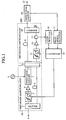
- Fig. 1 is a block diagram showing a configuration of a feedforward amplifier disclosed in Japanese patent application publication No. 7-77330.
- the technique is an example that injects the pilot signal into the feedforward distortion compensation system to control the feedforward system.
- the reference numeral 101 designates a distortion detecting loop that includes the splitter 2, first vector regulator 3, main amplifier 4, delay circuit 5 and splitter/combiner 6 , and cancels the input signal component by combining the input signal with the output of the main amplifier 4, thereby extracting a distortion component generated by the main amplifier 4.
- the pilot signal supplied from the pilot signal generator 8 is injected into the output of the main amplifier 4 via the directional coupler 7.
- the pilot signal is used for controlling a distortion canceling loop 102 as described later.
- the output signal of the main amplifier 4 passes through the splitter/combiner 6, and its major part passing through the delay circuit 9 is supplied to a first input terminal of the combiner 10 installed on the output side.
- the distortion component extracted by the distortion detecting loop 101 appears at a terminal of the splitter/combiner 6, passes through the second vector regulator 11, is amplified by the auxiliary amplifier 12, and is input to the second input terminal of the combiner 10.
- the combiner 10 combines the output signal passing through the delay circuit 9 with the distortion component amplified by the auxiliary amplifier 12 in the same amplitude but in the opposite phase, thereby canceling the distortion component and producing the output of small distortion from the output terminal 15.
- the optimizing control of the distortion detecting loop 101 in the feedforward amplifier is carried out as follows by controlling the vector regulator 3.
- the directional coupler 13 connected to the output of the auxiliary amplifier 12 extracts a part of the signal, the level of which is detected by the level detector 16.
- the minimum power level of the signal indicates the best canceled state of the signal component, in which the distortion detecting loop 101 is controlled at the optimum state. Therefore, the controller 18 automatically controls the first vector regulator 3 such that the power level detected by the level detector 16 becomes minimum.
- the optimizing control of the distortion canceling loop 102 is carried out as follows by controlling the second vector regulator 11.
- the directional coupler 14 installed on the output side of the feedforward amplifier extracts a part of the output signal, and the pilot signal detector 17 detects the pilot signal included in the output signal.
- the minimum level of the pilot signal indicates the best regulated state of the distortion canceling loop 102. Therefore, the controller 18 automatically controls the second vector regulator 11 such that the pilot signal detected by the pilot signal detector 17 becomes minimum.
- the conventional feedforward amplifier implements the optimum distortion compensation against the ambient temperature variations and deterioration with age by optimally controlling the two loops constituting the feedforward distortion compensation system, that is, the distortion detecting loop 101 and the distortion canceling loop 102.
- a filter is often connected to the output terminal of the feedforward amplifier to pass the desired signal and reject the frequency of the pilot signal.
- the frequency of the desired signal must be close to that of the pilot signal. Accordingly, it is unavoidable that the filter to separate them becomes large in size and loss, bringing about an increase in size and reduction in efficiency of the amplifier.
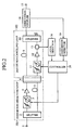
- Fig. 2 is a block diagram showing another configuration of the feedforward amplifier disclosed in Japanese patent application publication No. 7-77330.
- Fig. 2 the same or like portions to those of Fig. 1 are designated by the same reference numerals, and the description thereof is omitted here.
- This feedforward amplifier lacks the pilot signal generator 8 of Fig. 1. It supplies part of the output signal extracted by the directional coupler 14 to the distortion detector 19 for detecting the distortion of the output signal to control the feedforward system in such a manner that the distortion becomes minimum.
- This configuration has the following problem.
- the feedforward amplifier it is very difficult for the feedforward amplifier to carry out the control by detecting the distortion component of its output signal because the distortion component is usually much smaller than the signal component by a factor from 50 dB to 60 dB. Therefore, the distortion detector 19 cannot be realized in practice, or even if it is realized, its circuit configuration will be complicated, resulting in an increase in its size and cost.
- FIG. 3 is a block diagram showing a configuration of the feedforward amplifier.
- the same or like portions to those of Fig. 2 are designated by the same reference numerals, and the description thereof is omitted here.
- the reference numeral 103 designates a distortion detecting loop that comprises the splitters 2 and 25, the first vector regulator 3, the main amplifier 4, the delay circuit 5 and the splitter/combiner 6.
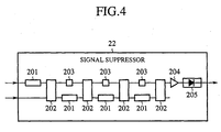
- Fig. 4 is a block diagram showing a configuration of the signal suppressor 22 as shown in Fig. 3.
- the reference numeral 201 designates a vector regulator
- 202 designates a splitter/combiner
- 203 designates a delay circuit
- 204 designates an amplifier
- 205 designates a level detector.
- the feedforward amplifier detects the distortion component signal extracted by the directional coupler 13 by the level detector 21, and controls the first vector regulator 3 by the controller 20 such that the power level of the distortion component signal becomes minimum, thereby carrying out the optimum control of the distortion detecting loop 103.
- the directional coupler 13 is installed before the second vector regulator 11 in Fig. 3, it can be provided after the auxiliary amplifier 12 as in Fig. 1 because the scheme of the optimizing control of the distortion detecting loop 103 is the same as that of Fig. 1.
- the pilot signal generator 8 as shown in Fig. 1 is not installed. Instead, the splitter 25 provided on the input side of the feedforward amplifier extracts a part of the input signal, and supplies it to the signal suppressor 22 via the delay circuit 24. In addition, the directional coupler 14 on the output side of the feedforward amplifier extracts a part of the output signal, and supplies it to the signal suppressor 22.
- the signal suppressor 22 has an internal configuration as shown in Fig. 4.
- the input signal and output signal of the feedforward amplifier supplied to the signal suppressor 22 are combined by the signal suppressor 22 with the internal configuration including the multi-staged vector regulators 201, splitter/combiners 202 and delay circuits 203.
- Using the multi-stage internal configuration of the signal suppressor can cancel out the signal component by a factor of 50 dB to 60 dB, leaving the distortion component included in the feedforward amplifier.
- the distortion component is amplified by the amplifier 204, and detected by the level detector 205.
- the controller 23 controls the second vector regulator 11 such that the power level of the distortion component is reduced, thereby carrying out the optimizing control of the distortion canceling loop 102.
- the conventional feedforward amplifier has a problem of increasing size and complexity because it employs the signal suppressor 22 including the multi-staged splitter/combiners 202, vector regulators 201 and delay circuit 203. In addition, it has a problem in that the adjustment is tedious of the many vector regulators 201 and delay circuits 203 included in the signal suppressor 22.
- the conventional feedforward amplifiers with the foregoing configurations have the following problems.
- the feedforward amplifiers that control their feedforward system by injecting the pilot signal have a problem of outputting the residual pilot signal resulting from the control process from the output terminal.
- the present invention is implemented to solve the foregoing problems. Therefore, it is an object of the present invention to provide a feedforward amplifier that can implement favorable distortion characteristic unaffected by the variations in the ambient temperature or deterioration with age, and that has a small size and high efficiency, and can cope with the frequency changes with ease.
- a feedforward amplifier that includes a distortion detecting loop having a first vector regulator, and a distortion canceling loop having a second vector regulator, and that carries out feedforward distortion compensation
- the feedforward amplifier comprising: a directional coupler for extracting a part of an output signal; a first splitter for extracting a part of an input signal; a delay circuit for delaying the input signal extracted by the first splitter; a combiner for combining the input signal delayed by the delay circuit with the output signal extracted by the directional coupler; a local oscillator for generating a signal of a prescribed frequency; a frequency converter for down-converting an output of the combiner to a low frequency using the signal generated by the local oscillator; a first filter for passing a distortion component and for rejecting a signal component of an output of the frequency converter; a distortion component detector for measuring the distortion component output from the first filter; and a second vector regulator controller for controlling the second vector regulator of the distortion canceling loop such that the distortion
- the feedforward amplifier can obviate the need for employing a circuit configuration operating at a high frequency in the control for minimizing the distortion component of the second vector regulator in the distortion canceling loop.
- This offers an advantage of being able to facilitate implementing the favorable distortion characteristic resistant to variations in the ambient temperature or deterioration with age, to facilitate reduction in size and increase in efficiency, and to cope with the frequency change of the input signal by varying the local oscillation frequency used for the frequency conversion that converts the output of the combiner to the low frequency by the frequency converter.
- the feedforward amplifier can further comprise: a third vector regulator interposed between the delay circuit and the combiner for changing pass amplitude and pass phase of an output of the delay circuit; a second splitter interposed between the combiner and the first filter for dividing a signal supplied to it; a second filter for passing a signal component and for rejecting a distortion component of a signal delivered by the second splitter; a signal component detector for measuring the signal component output from the second filter; and a third vector regulator controller for controlling the third vector regulator such that the signal component measured by the signal component detector becomes minimum.
- a third vector regulator interposed between the delay circuit and the combiner for changing pass amplitude and pass phase of an output of the delay circuit
- a second splitter interposed between the combiner and the first filter for dividing a signal supplied to it
- a second filter for passing a signal component and for rejecting a distortion component of a signal delivered by the second splitter
- a signal component detector for measuring the signal component output from the second filter
- a third vector regulator controller for controlling the
- the feedforward amplifier can obviate the need for the distortion component detector and signal component detector to measure the distortion component and signal component at the radio frequency.
- This offers an advantage of being able to improve the detection accuracy, and to cancel out the signal component without failure at high accuracy using the input signal and output signal in spite of the variations in the circuit characteristic due to the deterioration with age or ambient temperature variations, thereby implementing good feedforward distortion compensation.
- the feedforward amplifier can further comprise: a third vector regulator interposed between the delay circuit and the combiner for changing pass amplitude and pass phase of an output of the delay circuit; a second splitter interposed between the combiner and the first filter for dividing a signal supplied to it; a signal component detector for measuring a signal component delivered by the second splitter; and a third vector regulator controller for controlling the third vector regulator such that the signal component measured by the signal component detector becomes minimum.
- the feedforward amplifier can obviate the second filter for passing the signal component and for rejecting the distortion component of the first low frequency.signal distributed by the second splitter, which offers an advantage of being able to implement the feedforward amplifier with the reduced size and cost by an amount of removing the second filter.
- the second splitter can be interposed between the combiner and the frequency converter.
- the feedforward amplifier can detect in the radio frequency band the output power obtained by combining the output of the third vector regulator and the part of the output signal extracted by the directional coupler. It offers an advantage of being able to implement the cancellation of the signal component by the combining at practical accuracy, and to carry out the control of the feedforward distortion compensation system at high accuracy.
- the distortion detecting loop can comprise an input side splitter for dividing the input signal, and a main amplifier for amplifying a first part of the input signal divided by the input side splitter, wherein the first splitter can further divide a second part of the input signal divided by the input side splitter.
- the feedforward amplifier can obviate the need for installing a splitter on the main path of the input signal from the input terminal of the feedforward amplifier to the splitter/combiner via the main amplifier, that is, on the path of the signal constituting the major part of the output signal of the feedforward amplifier.
- it offers an advantage of being able to prevent the reduction in the total gain of the amplifier due to the loss of the splitter, and to implement a favorable distortion characteristic resistant to the variations in the ambient temperature or deterioration with age.
- the distortion detecting loop can comprise an input side splitter for dividing the input signal, a main amplifier for amplifying a first part of the input signal divided by the input side splitter, and an intra-distortion-detecting-loop delay circuit for delaying a second part of the input signal divided by the input side splitter, wherein the first splitter can be interposed into a path on an output side of the intra-distortion-detecting-loop delay circuit.
- the feedforward amplifier can utilize the delay circuit in the distortion detecting loop as a part of the delay circuit for delaying the input signal, which is installed on the path of the input signal to be combined with the output signal.
- it offers an advantage of being able to miniaturize the delay circuit by an amount corresponding to the delay the input signal undergoes through the delay circuit in the distortion detecting loop, thereby reducing the total size of the amplifier.
- a feedforward amplifier that includes a distortion detecting loop having a first vector regulator, and a distortion canceling loop having a second vector regulator, and that carries out feedforward distortion compensation
- the feedforward amplifier comprising: a first splitter for extracting a part of an input signal; a delay circuit for delaying the input signal extracted by the first splitter; a third vector regulator for changing pass amplitude and pass phase of an output of the delay circuit; a local oscillator for generating a signal of a prescribed frequency; a first frequency converter for down-converting an output of the third vector regulator to a low frequency using the signal generated by the local oscillator; a directional coupler for extracting a part of an output signal; a second frequency converter for down-converting an output of the directional coupler to a low frequency using the signal generated by the local oscillator; a combiner for combining an output of the first frequency converter and an output of the second frequency converter; a second splitter for dividing an output of the
- the feedforward amplifier can obviate the need for employing radio frequency connecting wire as the connecting wire on the input side of the combiner that combines the output of the third vector regulator and the output signal extracted by the directional coupler, thereby miniaturizing the amplifier.
- the feedforward amplifier can utilize a low frequency circuit configuration after combining the output of the third vector regulator and the output signal extracted by the directional coupler. Thus, it offers an advantage of being able facilitate reducing the size and cost of the amplifier.
- a feedforward amplifier that includes a distortion detecting loop having a first vector regulator, and a distortion canceling loop having a second vector regulator, and that carries out feedforward distortion compensation
- the feedforward amplifier comprising: a first splitter for extracting a part of an input signal; a local oscillator for generating a signal of a prescribed frequency; a first frequency converter for down-converting the input signal extracted by the first splitter to a low frequency using the signal generated by the local oscillator; a delay circuit for delaying an output signal of the first frequency converter; a third vector regulator for changing pass amplitude and pass phase of an output of the delay circuit; a directional coupler for extracting a part of an output signal; a second frequency converter for down-converting an output of the directional coupler to a low frequency using the signal generated by the local oscillator; a combiner for combining an output of the second frequency converter and a signal passing through the third vector regulator; a second splitter for dividing an
- the feedforward amplifier can configure all the circuit components after the frequency conversion by using the low frequency components.
- it offers an advantage of being able to facilitate reducing the size and cost of the amplifier.
- Fig. 5 is a block diagram showing a configuration of an embodiment 1 of the feedforward amplifier in accordance with the present invention.
- the reference numeral 1 designates an input terminal of the amplifier; 2 designates a splitter (input side splitter) for delivering the input signal supplied from the input terminal 1 to two paths; 3 designates a first vector regulator for electrically adjusting the amplitude and phase of the signal passing through the first path; 4 designates a main amplifier for amplifying the input signal; 5 designates a delay circuit (a delay circuit in the distortion detecting loop) for delaying the input signal that is delivered by the splitter 2 and passes through the second path; and 6 designates a splitter/combiner for dividing a part of the output signal of the main amplifier 4, for supplying a first part of that signal to the delay circuit 9, and for combining a second part of the signal and the part of the input signal passing through the delay circuit 5 to be supplied to a directional coupler 13.
- the reference numeral 103 designates a distortion detecting loop comprising the splitters 2 and 25, the first vector regulator 3, the main amplifier 4, the delay circuit 5 and the splitter/combiner 6. It cancels out the input signal component by combining the input signal with the output of the main amplifier 4, thereby extracting the distortion component of the main amplifier 4.
- the reference numeral 14 designates a directional coupler; and 15 designates an output terminal of the amplifier.
- the output signal of the main amplifier 4 passes through the splitter/combiner 6, and the major part thereof passes through the delay circuit 9 to be supplied to the first input terminal of the combiner 10 installed on the output side.
- the distortion component extracted by the distortion detecting loop 103 appears at a terminal of the splitter/combiner 6, passes through the directional coupler 13 and second vector regulator 11, and is amplified by the auxiliary amplifier 12 to be input to the second input terminal of the combiner 10.
- the combiner 10 combines the output signal passing through the delay circuit 9 with the distortion component amplified by the auxiliary amplifier 12 in the same amplitude but in the opposite phase to cancel the distortion component, thereby producing the output with little distortion from the output terminal 15.
- the feedforward amplifier carries out the optimizing control of the distortion detecting loop 103 as follows by controlling the vector regulator 3.
- the level detector 21 detects the distortion component signal extracted by the directional coupler 13, and the controller 20 controls the first vector regulator 3 such that the power level of the distortion component becomes minimum.
- the optimum control of the distortion detecting loop 103 is carried out.
- the directional coupler 13 can be installed after the auxiliary amplifier 12 without any problem.
- the combiner 51 is supplied with the part of the signal extracted by the splitter 25 installed at the input side of the feedforward amplifier via the delay circuit 24.
- the combiner 51 is also supplied with the part of the output signal of the feedforward amplifier from the directional coupler 14 on the output side.
- the combiner 51 combines the output signal of the feedforward amplifier supplied from the directional coupler 14 with the input signal extracted by the splitter 25 installed at the input side.
- the delay circuit 24 is installed to place the input signal and the output signal in the opposite phase but in the same amplitude at the combiner 51.
- the frequency converter 53 down-converts the output of the combiner 51 to a sufficiently lower frequency using the output of the local oscillator 52, and the filter 54, rejecting the signal component and passing the distortion component, extracts only the distortion component.
- the power of the distortion component is detected by the power detector 55.
- the distortion canceling loop 102 is adjusted to the optimum state of the feedforward distortion compensation system. Therefore, the controller 56 controls the second vector regulator 11 such that the power detected by the power detector 55 becomes minimum.
- the present embodiment 1 since the present embodiment 1 does not use the pilot signal, the pilot signal is not produced from the output terminal 15. Thus, the present embodiment 1 can obviate the filter for eliminating the pilot signal, and offers an advantage of being able to miniaturize the feedforward amplifier with ease.
- the present embodiment 1 can prevent the efficiency of the amplifier from being decreased by the loss of the filter, it can configure a high efficiency amplifier, thereby offering an advantage of being able to promote the miniaturization and improve the efficiency of devices utilizing the feedforward amplifier.
- the present embodiment 1 cancels out the signal component by the combiner 51 that combines the input signal extracted by the splitter 25 with the output signal extracted by the directional coupler 14, the power difference between the frequency components of the signal and of the distortion passing through the filter 54 can be a feasible value from 30 dB to 40 dB, for example.
- it offers an advantage of being able to implement the feedforward amplifier enabling the reduction in its size and cost.
- the present embodiment 1 detects the power of the distortion component using the low frequency filter 54 after down-converting the radio-frequency signal to the low frequency by the frequency converter 53, it is unnecessary to achieve signal suppression of about 60 dB in the radio frequency as the feedforward amplifier of Figs. 3 and 4, but the suppression of about 30 dB is sufficient. Therefore, the multi-stage signal suppressor 22 as shown in Fig. 4 is not required, offering an advantage of being able to implement a small size, practical feedforward amplifier.
- the present embodiment 1 can easily cope with the frequency change in amplification by varying the oscillation frequency of the local oscillator 52.
- employing a voltage controlled oscillator (VCO) as the local oscillator 52 enables the oscillation frequency to be electrically controlled easily, offering an advantage of being able to implement a feedforward amplifier that can flexibly deal with the change in the amplification frequency.
- VCO voltage controlled oscillator
- Fig. 6 is a block diagram showing a configuration of an embodiment 2 of the feedforward amplifier.
- Fig. 6 the same or like portions to those of Fig. 5 are designated by the same reference numerals, and the description thereof is omitted here.
- Fig. 6 the same or like portions to those of Fig. 5 are designated by the same reference numerals, and the description thereof is omitted here.
- the reference numeral 57 designates a splitter (second splitter) interposed between the combiner 51 and the filter 54 for dividing the signal; 58 designates a filter (second filter), a bandpass filter for rejecting the distortion component and passing the signal component of the signal delivered by the splitter 57; 59 designates a power detector (signal component detector) for measuring the power of the signal component output from the filter 58; 60 designates a controller (third vector regulator controller) for controlling a third vector regulator 61 such that the signal component measured by the power detector 59 becomes. minimum; and 61 designates the third vector regulator.
- a part of the input signal divided by the splitter 25 passes through the delay circuit 24 and the third vector regulator 61 to be supplied to the combiner 51.
- the combiner 51 combines the input signal with the output signal extracted by the directional coupler 14, and the frequency converter 53 down-converts the output of the combiner 51.
- the splitter 57 delivers a first part of the output of the frequency converter 53 to the filter 54 that passes only the distortion component to be detected by the power detector 55.
- the splitter 57 supplies a second part of the output to the filter 58 so that the power detector 59 detects the power level of the signal component.
- the controller 60 controls the third vector regulator 61 such that the power level detected by the power detector 59 becomes minimum.
- the power detector 55 detects its power level and supplies it to the controller 56 that controls the second vector regulator 11 such that the power level becomes minimum.
- the control of the second vector regulator 11 by the controller 56 is carried out independently of the control of the third vector regulator 61 by the controller 60.
- the third vector regulator 61 is installed on the path on the input signal side, it can be interposed into the path on the output signal side from the directional coupler 14.
- the present embodiment 2 can achieve similar advantages of the embodiment 1. In addition, it can always carry out the cancellation of the signal component at high accuracy by the combiner 51 using the input signal and output signal, in spite of the changes in the characteristics of the splitter 25, delay circuit 24, directional coupler 14 and combiner 51 due to the deterioration with age or ambient temperature variations.
- the present embodiment 2 can reduce the residual signal component due to insufficient cancellation to a favorable level, and reduce the (adverse) effect of the residual signal component on the power detection of the distortion component by the power detector 55. Therefore, the power detector 55 can detect the power of the distortion component at high detection accuracy, and the controller 56 can control the second vector regulator 11 satisfactorily, thereby always maintaining the feedforward distortion compensation at a good condition.
- the combiner 51 can always cancel the signal component at high accuracy, thereby implementing satisfactory feedforward distortion compensation.
- Fig. 7 is a block diagram showing a configuration of the present embodiment 3 of the feedforward amplifier.
- Fig. 7 the same or like portions to those of Fig. 6 are designated by the same reference numerals, and the description thereof is omitted here.
- the present embodiment 3 of the feedforward amplifier is configured by eliminating the filter 58 for passing the signal frequency component from the configuration as shown in Fig. 6.
- the accuracy of the cancellation of the signal component by the combiner 51 is determined by the accuracy of the components of the system, and is about 30 dB at best. Accordingly, the signal component occupies the major portion of the output of the frequency converter 53. As a result, it usually presents little problem to eliminate the filter for passing only the signal component from before the power detector 59 for detecting the power level of the signal component.
- the configuration as shown in Fig. 7 that removes the filter 58 for passing the signal frequency component from the configuration as shown in Fig. 6 can not only achieve the advantages of the foregoing embodiment 2, but also offer an advantage of being able to implement the reduction in size and cost of the feedforward amplifier.
- Fig. 8 is a block diagram showing a configuration of the present embodiment 4 of the feedforward amplifier.
- the same or like portions to those of Fig. 7 are designated by the same reference numerals, and the description thereof is omitted here.
- the reference numeral 62 designates a splitter (second splitter) for dividing the output of the combiner 51; and 63 designates a radio-frequency power detector (signal component detector) for detecting the power of the signal delivered by the splitter 62.
- the output of the combiner 51 is divided by the splitter 62, and the first part thereof is supplied to the frequency converter 53 that down-converts it to the low frequency.
- the low frequency signal passes through the filter 54 for passing the distortion component frequency and is supplied to the power detector 55 so that the controller 56 controls the second vector regulator 11 such that the power level of the distortion component detected by the power detector 55 becomes minimum.
- the second part delivered by the splitter 62 is directly supplied to the radio-frequency power detector 63 that detects its power level.
- the controller 60 controls the third vector regulator 61 such that the power level becomes minimum to reduce the signal component in the output of the combiner 51, thereby improving the detection accuracy of the distortion component by the level detector 21.
- the present embodiment 4 directly detects the output power of the combiner 51 in the radio frequency band, and controls the third vector regulator 61 such that the power becomes minimum.
- the present embodiment 4 can implement the cancellation of the signal component by the combiner 51 at practical accuracy, offering an advantage of being able to provide the feedforward amplifier capable of controlling the feedforward distortion compensation system at high accuracy.
- Fig. 9 is a block diagram showing a configuration of the present embodiment 5 of the feedforward amplifier.
- the same or like portions to those of Fig. 6 are designated by the same reference numerals, and the description thereof is omitted here.
- the reference numeral 64 designates a frequency converter (second frequency converter) for down-converting the output signal split by the directional coupler 14 to a low frequency using the signal output from the local oscillator 52;
- 65 designates a frequency converter (first frequency converter) for down-converting the output of the third vector regulator 61 to a low frequency using the signal output from the local oscillator 52;
- 66 designates a combiner for combining the outputs of the frequency converters 64 and 65.
- a part of the input signal divided by the splitter 25 passes through the delay circuit 24 and the third vector regulator 61, and is down-converted to the low frequency signal by the frequency converter 65.
- a part of the output signal extracted by the directional coupler 14 is down-converted to the low frequency signal by the frequency converter 64.
- the combiner 66 combines the outputs of the frequency converters 64 and 65 in the same amplitude but in the opposite phase to cancel out the signal component.
- the output signal of the combiner 66 is divided into two portions by the splitter 57. The first portion passes through the filter 54 that passes only the distortion component frequency, and is supplied to the power detector 55. The second portion passes through the filter 58 that passes only the signal component frequency, and is supplied to the power detector 59.
- controllers 56 and 60 control the second vector regulator 11 and third vector regulator 61, respectively.
- the present embodiment 5 of the feedforward amplifier differs from the foregoing embodiment 2 in that the combiner 66 combines the two low frequency signals, that is, the input signal divided by the splitter 25 and the output signal extracted by the directional coupler 14, to extract the distortion component by canceling out the signal component. Accordingly, the combiner 66 can be a combiner for the low frequency.
- the present embodiment 5 offers the same advantages of the foregoing embodiment 2.
- it can obviate the radio-frequency connecting wire on the input side of the combiner 66, thereby offering an advantage of being able to provide greater flexibility of wiring, and by extension to miniaturize the device.
- the present embodiment 5 can implement the circuit configuration using the low frequency combiner 66, splitter 57 and filters 54 and 58, making it easier to integrate them into an IC.
- it offers an advantage of being able to implement the feedforward amplifier that can reduce its size and cost with ease.
- Fig. 10 is a block diagram showing a configuration of the present embodiment 6 of the feedforward amplifier.
- the same or like portions to those of Fig. 9 are designated by the same reference numerals, and the description thereof is omitted here.
- the reference numeral 67 designates a frequency converter (first frequency converter) for down-converting a part of the input signal divided by the splitter 25 by using the output signal from the local oscillator 52;
- 68 designates a low frequency delay circuit for delaying the output of the frequency converter 67;
- 69 designates a low frequency vector regulator for adjusting the pass amplitude and pass phase of the output of the delay circuit 68.
- the present embodiment 6 of the feedforward amplifier differs from the foregoing embodiment 5 in that the part of the input signal divided by the input side splitter 25 is immediately down-converted to the low frequency by the frequency converter 67.
- the output of the frequency converter 67 passes through the low frequency delay circuit 68 and the low frequency vector regulator 69, and is supplied to the combiner 66.
- the subsequent operation is the same as that of the foregoing embodiment 5.
- the present embodiment 6 can achieve the same advantages as the foregoing embodiment 5.
- the present embodiment 6 can utilize low frequency components for the delay circuit 68 and the vector regulator 69, which are fabricated easier than those of the radio-frequency counterparts.
- the vector regulator can be configured using a signal processing circuit (DSP: Digital Signal Processor) which can provide greater flexibility to the vector regulator, making it easier to miniaturize and adjust the vector regulator, and by extension to reduce the size of the feedforward amplifier and to improve the distortion characteristic.
- DSP Digital Signal Processor
- the present embodiment 6 offers an advantage of being able to implement the feedforward amplifier with a reduced size and cost.
- Fig. 11 is a block diagram showing a configuration of the present embodiment 7 of the feedforward amplifier.
- the same or like portions to those of Fig. 6 are designated by the same reference numerals, and the description thereof is omitted here.
- the reference numeral 71 designates a splitter (first splitter) interposed between the splitter 2 and the delay circuit 5 for further dividing the part of the input signal divided by the splitter 2.
- the present embodiment 7 of the feedforward amplifier differs from the foregoing embodiment 2 in that it comprises the splitter 71, which is interposed between the splitter 2 and the delay circuit 5 for further dividing the part of the input signal divided by the splitter 2, instead of the splitter 25 for dividing the input signal supplied from the input terminal 1.
- the foregoing configuration can remove the splitter 25 from the main path of the input signal from the input terminal 1 to the splitter/combiner 6 via the main amplifier 4, that is, the path of the major part of the signal to become the output signal of the feedforward amplifier, thereby preventing the reduction in the total gain of the amplifier due to the loss of the splitter 25.
- Fig. 11 changes the position of the splitter 25 for dividing the input signal in the foregoing embodiment 2, the foregoing embodiments 1, and 3-6 can also offer the same advantage as the present embodiment 7 by changing the position of their splitter 25.
- Fig. 12 is a block diagram showing a configuration of the present embodiment 8 of the feedforward amplifier.
- the same or like portions to those of Fig. 6 are designated by the same reference numerals, and the description thereof is omitted here.
- the reference numeral 72 designates a splitter interposed into the path on the output side of the delay circuit 5 for further dividing a part of the input signal divided by the splitter 2 and passing through the delay circuit 5.
- the present embodiment 8 of the feedforward amplifier differs from the foregoing embodiment 2 in that it comprises the splitter 72, which is interposed into the path on the output side of the delay circuit 5 for further dividing the part of the input signal divided by the splitter 2 and passing through the delay circuit 5, instead of the splitter 25 for dividing the input signal supplied from the input terminal 1.
- This configuration makes it possible for the delay circuit 5 to share the function of the delay circuit 24 in part, reducing the delay time of the delay circuit 24. Thus, it is possible to reduce the size of the delay circuit 24, and by extension to reduce the size of the device.
- Fig. 12 utilizes the splitter 72 interposed into the path on the output side of the delay circuit 5 in place of the splitter 25 for dividing the input signal in the foregoing embodiment 2, the foregoing embodiments 1, and 3-6 can also offer the same advantage as the present embodiment 8 by changing the position of their splitter 25 to the output side of the delay circuit 5.
- the feedforward amplifier in accordance with the present invention can be preferably applied to the low distortion amplification in a radio frequency band such as VHF, UHF and microwave frequency bands for implementing favorable distortion compensation without being affected by the ambient temperature or deterioration with age.
- a radio frequency band such as VHF, UHF and microwave frequency bands
Landscapes
- Physics & Mathematics (AREA)
- Nonlinear Science (AREA)
- Engineering & Computer Science (AREA)
- Power Engineering (AREA)
- Amplifiers (AREA)
Abstract
A delayed input
signal from a delay circuit
(24) and an output signal are
combined by a combiner (51).
The output form combiner (51)
is converted into a low-frequency
signal by a frequency converter
(53). Distortion components
are extracted from the output
from the frequency converter
(53) and measured by a power
detector (55). A control circuit
(56) controls a second vector
controller (11) in a distortion
cancel loop (102) to minimize the
measured distortion components.
Description
The present invention relates to a feedforward amplifier for
carrying out low distortion amplification in a radio frequency band.
A feedforward amplifier that achieves a low distortion
characteristic by feedforward distortion compensation is often used
as an amplifier for carrying out low distortion amplification in a
radio frequency band such as VHF, UHF and microwave frequency bands.
The feedforward distortion compensation can implement favorable
distortion compensation in principle, and has an advantage of being
able to configure a very low distortion, small amplifier. However,
it has a problem in that when the characteristic of the amplifier varies
because of ambient temperature or deterioration with age, its
distortion compensation range is reduced and the distortion
characteristic is impaired significantly.
To solve the problem, a method is proposed that injects a pilot
signal into a loop constituting the feedforward distortion
compensation system, and controls the amplifier or the loop
constituting the feedforward system by detecting the pilot signal.
Fig. 1 is a block diagram showing a configuration of a feedforward
amplifier disclosed in Japanese patent application publication No.
7-77330. The technique is an example that injects the pilot signal
into the feedforward distortion compensation system to control the
feedforward system.
In Fig. 1, the reference numeral 1 designates an input terminal
of the amplifier; 2 designates a splitter for distributing an input
signal to two paths; 3 designates a first vector regulator for
electrically regulating the amplitude and phase of a signal passing
through the first path; 4 designates a main amplifier for amplifying
the input signal; 5 designates a delay circuit for delaying the input
signal distributed to the second path by the splitter 2; 6 designates
a splitter/combiner for distributing a part of the output signal of
the main amplifier 4 and for combining the distributed output signal
with a part of the input signal passing through the delay circuit 5;
7 designates a directional coupler; and 8 designates a pilot signal
generator.
The reference numeral 101 designates a distortion detecting loop
that includes the splitter 2, first vector regulator 3, main amplifier
4, delay circuit 5 and splitter/combiner 6 , and cancels the input
signal component by combining the input signal with the output of the
main amplifier 4, thereby extracting a distortion component generated
by the main amplifier 4. Here, the pilot signal supplied from the
pilot signal generator 8 is injected into the output of the main
amplifier 4 via the directional coupler 7. The pilot signal is used
for controlling a distortion canceling loop 102 as described later.
The reference numeral 9 designates a delay circuit; 10 designates
a combiner; 11 designates a second vector regulator; 12 designates
an auxiliary amplifier; 13 designates a directional coupler; 102
designates the distortion canceling loop including the delay circuit
9, combiner 10, second vector regulator 11, auxiliary amplifier 12
and directional coupler 13. The reference numeral 14 designates a
directional coupler; 15 designates an output terminal of the
amplifier; 16 designates a level detector; 17 designates a pilot signal
detector; and 18 designates a controller for controlling the first
vector regulator 3 and the second vector regulator 11.
Next, the operation of the conventional feedforward amplifier
will be described.
The output signal of the main amplifier 4 passes through the
splitter/combiner 6, and its major part passing through the delay
circuit 9 is supplied to a first input terminal of the combiner 10
installed on the output side. The distortion component extracted by
the distortion detecting loop 101 appears at a terminal of the
splitter/combiner 6, passes through the second vector regulator 11,
is amplified by the auxiliary amplifier 12, and is input to the second
input terminal of the combiner 10. The combiner 10 combines the output
signal passing through the delay circuit 9 with the distortion
component amplified by the auxiliary amplifier 12 in the same amplitude
but in the opposite phase, thereby canceling the distortion component
and producing the output of small distortion from the output terminal
15.
The optimizing control of the distortion detecting loop 101 in
the feedforward amplifier is carried out as follows by controlling
the vector regulator 3.
The directional coupler 13 connected to the output of the
auxiliary amplifier 12 extracts a part of the signal, the level of
which is detected by the level detector 16. The minimum power level
of the signal indicates the best canceled state of the signal component,
in which the distortion detecting loop 101 is controlled at the optimum
state. Therefore, the controller 18 automatically controls the first
vector regulator 3 such that the power level detected by the level
detector 16 becomes minimum.
Besides, the optimizing control of the distortion canceling loop
102 is carried out as follows by controlling the second vector
regulator 11.
The directional coupler 14 installed on the output side of the
feedforward amplifier extracts a part of the output signal, and the
pilot signal detector 17 detects the pilot signal included in the
output signal. The minimum level of the pilot signal indicates the
best regulated state of the distortion canceling loop 102. Therefore,
the controller 18 automatically controls the second vector regulator
11 such that the pilot signal detected by the pilot signal detector
17 becomes minimum.
Thus, the conventional feedforward amplifier implements the
optimum distortion compensation against the ambient temperature
variations and deterioration with age by optimally controlling the
two loops constituting the feedforward distortion compensation system,
that is, the distortion detecting loop 101 and the distortion canceling
loop 102.
As conventional feedforward amplifiers, many schemes other than
the foregoing method are proposed which carry out the control of the
feedforward system by injecting the pilot signal into the loop. All
these feedforward amplifiers exploiting the pilot signal have a common
problem in that they cannot help outputting the pilot signal from the
output terminal. Although the second vector regulator 11 is
controlled such that the pilot signal used for controlling the
distortion canceling loop 102 is canceled out in principle, the pilot
signal is not completely canceled in practice because of the limited
control accuracy or nonnegligible control time of the feedforward
system. Thus, it is unavoidable that the pilot signal is output from
the output terminal 15.
To solve this problem, a filter is often connected to the output
terminal of the feedforward amplifier to pass the desired signal and
reject the frequency of the pilot signal. However, to achieve the
control using the pilot signal at high accuracy, the frequency of the
desired signal must be close to that of the pilot signal. Accordingly,
it is unavoidable that the filter to separate them becomes large in
size and loss, bringing about an increase in size and reduction in
efficiency of the amplifier.
In view of this, some schemes are proposed that control the
feedforward distortion compensation system without utilizing the
pilot signal.
Fig. 2 is a block diagram showing another configuration of the
feedforward amplifier disclosed in Japanese patent application
publication No. 7-77330. In Fig. 2, the same or like portions to those
of Fig. 1 are designated by the same reference numerals, and the
description thereof is omitted here.
This feedforward amplifier lacks the pilot signal generator 8
of Fig. 1. It supplies part of the output signal extracted by the
directional coupler 14 to the distortion detector 19 for detecting
the distortion of the output signal to control the feedforward system
in such a manner that the distortion becomes minimum.
This configuration has the following problem.
Specifically, it is very difficult for the feedforward amplifier
to carry out the control by detecting the distortion component of its
output signal because the distortion component is usually much smaller
than the signal component by a factor from 50 dB to 60 dB. Therefore,
the distortion detector 19 cannot be realized in practice, or even
if it is realized, its circuit configuration will be complicated,
resulting in an increase in its size and cost.
Another conventional feedforward amplifier without using the
pilot signal is disclosed in Japanese patent application laid-open
No. 7-336153. Fig. 3 is a block diagram showing a configuration of
the feedforward amplifier. In Fig. 3, the same or like portions to
those of Fig. 2 are designated by the same reference numerals, and
the description thereof is omitted here. In Fig. 3, the reference
numeral 20 designates a controller for controlling the first vector
regulator 3; 21 designates a level detector; 22 designates a signal
suppressor; 23 designates a controller for controlling the second
vector regulator 11; 24 designates a delay circuit; and 25 designates
a splitter. The reference numeral 103 designates a distortion
detecting loop that comprises the splitters 2 and 25, the first vector
regulator 3, the main amplifier 4, the delay circuit 5 and the
splitter/combiner 6. Fig. 4 is a block diagram showing a configuration
of the signal suppressor 22 as shown in Fig. 3. In Fig. 4, the reference
numeral 201 designates a vector regulator, 202 designates a
splitter/combiner, 203 designates a delay circuit, 204 designates an
amplifier, and 205 designates a level detector.
The feedforward amplifier detects the distortion component
signal extracted by the directional coupler 13 by the level detector
21, and controls the first vector regulator 3 by the controller 20
such that the power level of the distortion component signal becomes
minimum, thereby carrying out the optimum control of the distortion
detecting loop 103. Although the directional coupler 13 is installed
before the second vector regulator 11 in Fig. 3, it can be provided
after the auxiliary amplifier 12 as in Fig. 1 because the scheme of
the optimizing control of the distortion detecting loop 103 is the
same as that of Fig. 1.
In Fig. 3, the pilot signal generator 8 as shown in Fig. 1 is
not installed. Instead, the splitter 25 provided on the input side
of the feedforward amplifier extracts a part of the input signal, and
supplies it to the signal suppressor 22 via the delay circuit 24. In
addition, the directional coupler 14 on the output side of the
feedforward amplifier extracts a part of the output signal, and
supplies it to the signal suppressor 22.
The signal suppressor 22 has an internal configuration as shown
in Fig. 4. The input signal and output signal of the feedforward
amplifier supplied to the signal suppressor 22 are combined by the
signal suppressor 22 with the internal configuration including the
multi-staged vector regulators 201, splitter/combiners 202 and delay
circuits 203. Using the multi-stage internal configuration of the
signal suppressor can cancel out the signal component by a factor of
50 dB to 60 dB, leaving the distortion component included in the
feedforward amplifier. The distortion component is amplified by the
amplifier 204, and detected by the level detector 205. The controller
23 controls the second vector regulator 11 such that the power level
of the distortion component is reduced, thereby carrying out the
optimizing control of the distortion canceling loop 102.
The conventional feedforward amplifier has a problem of
increasing size and complexity because it employs the signal
suppressor 22 including the multi-staged splitter/combiners 202,
vector regulators 201 and delay circuit 203. In addition, it has a
problem in that the adjustment is tedious of the many vector regulators
201 and delay circuits 203 included in the signal suppressor 22.
For example, even the slightest variations in the amplification
frequency involved in the change of the channels to be amplified by
the feedforward amplifier presents a problem of requiring
readjustment of all the vector regulators or all the delay circuits
of the signal suppressor 22.
In summary, the conventional feedforward amplifiers with the
foregoing configurations have the following problems. First, the
feedforward amplifiers that control their feedforward system by
injecting the pilot signal have a problem of outputting the residual
pilot signal resulting from the control process from the output
terminal.
Installing the output filter to eliminate the pilot signal
presents another problem of increasing the size and reducing the
efficiency of the amplifier because of the large size and loss of the
output filter.
As for the configuration as shown in Fig. 2 without the pilot
signal generator 8, which controls the feedforward system in such a
manner that the distortion becomes minimum by detecting the distortion
of the output signal, it is difficult to detect the distortion signal
smaller than the signal component by a factor of 50 dB to 60 dB to
carry out the control. Thus, it presents a problem in that the
distortion detector cannot be implemented in practice, or that even
if it can be implemented, its configuration will become complicated,
large and expensive.
As for the feedforward amplifier as shown in Figs. 3 and 4, it
presents a problem of increasing its size and complexity because of
the signal suppressor 22 with the multi-stage configuration.
In addition, since the slightest variations in the amplification
frequency requires the readjustment of all the vector regulators and
delay circuits of the signal suppressor 22, it has a problem of
requiring complicated adjustment in actual operation.
The present invention is implemented to solve the foregoing
problems. Therefore, it is an object of the present invention to
provide a feedforward amplifier that can implement favorable
distortion characteristic unaffected by the variations in the ambient
temperature or deterioration with age, and that has a small size and
high efficiency, and can cope with the frequency changes with ease.
According to a first aspect of the present invention, there is
provided a feedforward amplifier that includes a distortion detecting
loop having a first vector regulator, and a distortion canceling loop
having a second vector regulator, and that carries out feedforward
distortion compensation, the feedforward amplifier comprising: a
directional coupler for extracting a part of an output signal; a first
splitter for extracting a part of an input signal; a delay circuit
for delaying the input signal extracted by the first splitter; a
combiner for combining the input signal delayed by the delay circuit
with the output signal extracted by the directional coupler; a local
oscillator for generating a signal of a prescribed frequency; a
frequency converter for down-converting an output of the combiner to
a low frequency using the signal generated by the local oscillator;
a first filter for passing a distortion component and for rejecting
a signal component of an output of the frequency converter; a
distortion component detector for measuring the distortion component
output from the first filter; and a second vector regulator controller
for controlling the second vector regulator of the distortion
canceling loop such that the distortion component measured by the
distortion component detector becomes minimum.
According to this, the feedforward amplifier can obviate the
need for employing a circuit configuration operating at a high
frequency in the control for minimizing the distortion component of
the second vector regulator in the distortion canceling loop. This
offers an advantage of being able to facilitate implementing the
favorable distortion characteristic resistant to variations in the
ambient temperature or deterioration with age, to facilitate
reduction in size and increase in efficiency, and to cope with the
frequency change of the input signal by varying the local oscillation
frequency used for the frequency conversion that converts the output
of the combiner to the low frequency by the frequency converter.
Here, the feedforward amplifier can further comprise: a third
vector regulator interposed between the delay circuit and the combiner
for changing pass amplitude and pass phase of an output of the delay
circuit; a second splitter interposed between the combiner and the
first filter for dividing a signal supplied to it; a second filter
for passing a signal component and for rejecting a distortion component
of a signal delivered by the second splitter; a signal component
detector for measuring the signal component output from the second
filter; and a third vector regulator controller for controlling the
third vector regulator such that the signal component measured by the
signal component detector becomes minimum.
According to this, the feedforward amplifier can obviate the
need for the distortion component detector and signal component
detector to measure the distortion component and signal component at
the radio frequency. This offers an advantage of being able to improve
the detection accuracy, and to cancel out the signal component without
failure at high accuracy using the input signal and output signal in
spite of the variations in the circuit characteristic due to the
deterioration with age or ambient temperature variations, thereby
implementing good feedforward distortion compensation.
The feedforward amplifier can further comprise: a third vector
regulator interposed between the delay circuit and the combiner for
changing pass amplitude and pass phase of an output of the delay
circuit; a second splitter interposed between the combiner and the
first filter for dividing a signal supplied to it; a signal component
detector for measuring a signal component delivered by the second
splitter; and a third vector regulator controller for controlling the
third vector regulator such that the signal component measured by the
signal component detector becomes minimum.
According to this, the feedforward amplifier can obviate the
second filter for passing the signal component and for rejecting the
distortion component of the first low frequency.signal distributed
by the second splitter, which offers an advantage of being able to
implement the feedforward amplifier with the reduced size and cost
by an amount of removing the second filter.
The second splitter can be interposed between the combiner and
the frequency converter.
According to this, the feedforward amplifier can detect in the
radio frequency band the output power obtained by combining the output
of the third vector regulator and the part of the output signal
extracted by the directional coupler. It offers an advantage of being
able to implement the cancellation of the signal component by the
combining at practical accuracy, and to carry out the control of the
feedforward distortion compensation system at high accuracy.
The distortion detecting loop can comprise an input side splitter
for dividing the input signal, and a main amplifier for amplifying
a first part of the input signal divided by the input side splitter,
wherein the first splitter can further divide a second part of the
input signal divided by the input side splitter.
According to this, the feedforward amplifier can obviate the
need for installing a splitter on the main path of the input signal
from the input terminal of the feedforward amplifier to the
splitter/combiner via the main amplifier, that is, on the path of the
signal constituting the major part of the output signal of the
feedforward amplifier. Thus, it offers an advantage of being able
to prevent the reduction in the total gain of the amplifier due to
the loss of the splitter, and to implement a favorable distortion
characteristic resistant to the variations in the ambient temperature
or deterioration with age.
The distortion detecting loop can comprise an input side splitter
for dividing the input signal, a main amplifier for amplifying a first
part of the input signal divided by the input side splitter, and an
intra-distortion-detecting-loop delay circuit for delaying a second
part of the input signal divided by the input side splitter, wherein
the first splitter can be interposed into a path on an output side
of the intra-distortion-detecting-loop delay circuit.
According to this, the feedforward amplifier can utilize the
delay circuit in the distortion detecting loop as a part of the delay
circuit for delaying the input signal, which is installed on the path
of the input signal to be combined with the output signal. Thus, it
offers an advantage of being able to miniaturize the delay circuit
by an amount corresponding to the delay the input signal undergoes
through the delay circuit in the distortion detecting loop, thereby
reducing the total size of the amplifier.
According to a second aspect of the present invention, there
is provided a feedforward amplifier that includes a distortion
detecting loop having a first vector regulator, and a distortion
canceling loop having a second vector regulator, and that carries out
feedforward distortion compensation, the feedforward amplifier
comprising: a first splitter for extracting a part of an input signal;
a delay circuit for delaying the input signal extracted by the first
splitter; a third vector regulator for changing pass amplitude and
pass phase of an output of the delay circuit; a local oscillator for
generating a signal of a prescribed frequency; a first frequency
converter for down-converting an output of the third vector regulator
to a low frequency using the signal generated by the local oscillator;
a directional coupler for extracting a part of an output signal; a
second frequency converter for down-converting an output of the
directional coupler to a low frequency using the signal generated by
the local oscillator; a combiner for combining an output of the first
frequency converter and an output of the second frequency converter;
a second splitter for dividing an output of the combiner; a first filter
for passing a distortion component and for rejecting a signal component
of a first output of the second splitter; a distortion component
detector for measuring the distortion component output from the first
filter; a second vector regulator controller for controlling the
second vector regulator of the distortion canceling loop such that
the distortion component measured by the distortion component
detector becomes minimum; a second filter for passing a signal
component and for rejecting a distortion component of a second output
of the second splitter; a signal component detector for measuring the
signal component output from the second filter; and a third vector
regulator controller for controlling the third vector regulator such
that the signal component measured by the signal component detector
becomes minimum.
According to this, the feedforward amplifier can obviate the
need for employing radio frequency connecting wire as the connecting
wire on the input side of the combiner that combines the output of
the third vector regulator and the output signal extracted by the
directional coupler, thereby miniaturizing the amplifier. In
addition, the feedforward amplifier can utilize a low frequency
circuit configuration after combining the output of the third vector
regulator and the output signal extracted by the directional coupler.
Thus, it offers an advantage of being able facilitate reducing the
size and cost of the amplifier.
According to a third aspect of the present invention, there is
provided a feedforward amplifier that includes a distortion detecting
loop having a first vector regulator, and a distortion canceling loop
having a second vector regulator, and that carries out feedforward
distortion compensation, the feedforward amplifier comprising: a
first splitter for extracting a part of an input signal; a local
oscillator for generating a signal of a prescribed frequency; a first
frequency converter for down-converting the input signal extracted
by the first splitter to a low frequency using the signal generated
by the local oscillator; a delay circuit for delaying an output signal
of the first frequency converter; a third vector regulator for changing
pass amplitude and pass phase of an output of the delay circuit; a
directional coupler for extracting a part of an output signal; a second
frequency converter for down-converting an output of the directional
coupler to a low frequency using the signal generated by the local
oscillator; a combiner for combining an output of the second frequency
converter and a signal passing through the third vector regulator;
a second splitter for dividing an output of the combiner; a first filter
for passing a distortion component and for rejecting a signal component
of a first output of the second splitter; a distortion component
detector for measuring the distortion component output from the first
filter; a second vector regulator controller for controlling the
second vector regulator of the distortion canceling loop such that
the distortion component measured by the distortion component
detector becomes minimum; a second filter for passing a signal
component and for rejecting a distortion component of a second output
of the second splitter; a signal component detector for measuring the
signal component output from the second filter; and a third vector
regulator controller for controlling the third vector regulator such
that the signal component measured by the signal component detector
becomes minimum.
According to this, the feedforward amplifier can configure all
the circuit components after the frequency conversion by using the
low frequency components. Thus, it offers an advantage of being able
to facilitate reducing the size and cost of the amplifier.
The best mode for carrying out the present invention will now
be described with reference to the accompanying drawings.
Fig. 5 is a block diagram showing a configuration of an embodiment
1 of the feedforward amplifier in accordance with the present invention.
In Fig. 5, the reference numeral 1 designates an input terminal of
the amplifier; 2 designates a splitter (input side splitter) for
delivering the input signal supplied from the input terminal 1 to two
paths; 3 designates a first vector regulator for electrically
adjusting the amplitude and phase of the signal passing through the
first path; 4 designates a main amplifier for amplifying the input
signal; 5 designates a delay circuit (a delay circuit in the distortion
detecting loop) for delaying the input signal that is delivered by
the splitter 2 and passes through the second path; and 6 designates
a splitter/combiner for dividing a part of the output signal of the
main amplifier 4, for supplying a first part of that signal to the
delay circuit 9, and for combining a second part of the signal and
the part of the input signal passing through the delay circuit 5 to
be supplied to a directional coupler 13.
The reference numeral 103 designates a distortion detecting loop
comprising the splitters 2 and 25, the first vector regulator 3, the
main amplifier 4, the delay circuit 5 and the splitter/combiner 6.
It cancels out the input signal component by combining the input signal
with the output of the main amplifier 4, thereby extracting the
distortion component of the main amplifier 4.
The reference numeral 9 designates the delay circuit; 10
designates a combiner; 11 designates a second vector regulator; 12
designates an auxiliary amplifier; 13 designates the directional
coupler for extracting part of the output signal; 102 designates a
distortion canceling loop comprising the delay circuit 9, the combiner
10, the second vector regulator 11, the auxiliary amplifier 12 and
the directional coupler 13. The reference numeral 14 designates a
directional coupler; and 15 designates an output terminal of the
amplifier. The reference numeral 20 designates a controller for
controlling the first vector regulator 3; 21 designates a level
detector; 24 designates a delay circuit for delaying the input signal
extracted by a splitter 25; and 25 designates the splitter (first
splitter) for extracting a part of the input signal.
The reference numeral 51 designates a combiner for combining
the input signal delayed by the delay circuit 24 with the output signal
extracted by the directional coupler 14; 52 designates a local
oscillator for generating a signal of a prescribed frequency; 53
designates a frequency converter for down-converting the output of
the combiner 51 to a low frequency signal using the signal output from
the local oscillator 52; 54 designates a filter (first filter), a
bandpass filter for rejecting the signal component and for passing
the distortion component of the signal output from the frequency
converter 53; 55 designates a power detector (distortion component
detector) for measuring the distortion component output from the
filter 54; and 56 designates a controller (second vector regulator
controller) for controlling the second vector regulator 11 of the
distortion canceling loop 102 such that the distortion component
detected by the power detector 55 becomes minimum.
Next, the operation of the present embodiment 1 will be
described.
In the present embodiment 1 of the feedforward amplifier, the
output signal of the main amplifier 4 passes through the
splitter/combiner 6, and the major part thereof passes through the
delay circuit 9 to be supplied to the first input terminal of the
combiner 10 installed on the output side. The distortion component
extracted by the distortion detecting loop 103 appears at a terminal
of the splitter/combiner 6, passes through the directional coupler
13 and second vector regulator 11, and is amplified by the auxiliary
amplifier 12 to be input to the second input terminal of the combiner
10. The combiner 10 combines the output signal passing through the
delay circuit 9 with the distortion component amplified by the
auxiliary amplifier 12 in the same amplitude but in the opposite phase
to cancel the distortion component, thereby producing the output with
little distortion from the output terminal 15.
The feedforward amplifier carries out the optimizing control
of the distortion detecting loop 103 as follows by controlling the
vector regulator 3.
Specifically, the level detector 21 detects the distortion
component signal extracted by the directional coupler 13, and the
controller 20 controls the first vector regulator 3 such that the power
level of the distortion component becomes minimum. Thus, the optimum
control of the distortion detecting loop 103 is carried out. In this
case, the directional coupler 13 can be installed after the auxiliary
amplifier 12 without any problem.
On the other hand, the combiner 51 is supplied with the part
of the signal extracted by the splitter 25 installed at the input side
of the feedforward amplifier via the delay circuit 24. The combiner
51 is also supplied with the part of the output signal of the
feedforward amplifier from the directional coupler 14 on the output
side. Thus, the combiner 51 combines the output signal of the
feedforward amplifier supplied from the directional coupler 14 with
the input signal extracted by the splitter 25 installed at the input
side. By combining the input signal with the output signal in the
opposite phase but with the same amplitude, the signal component of
the output signal of the feedforward amplifier is canceled out, leaving
only the distortion component.
The delay circuit 24 is installed to place the input signal and
the output signal in the opposite phase but in the same amplitude at
the combiner 51.
To bring the input signal and output signal in the opposite phase
but in the same amplitude perfectly at the combiner 51 is difficult
because of the accuracy of the circuit components. It is practical
to assume that the signal component is canceled out by a factor of
about 30 dB. The ratio of the signal component to the distortion
component of the feedforward amplifier is from 50 dB to 60 dB.
Accordingly, the signal component is greater than the distortion
component by 20 dB to 30 dB even at the output of the combiner 51.
Taking account of this, the frequency converter 53 down-converts the
output of the combiner 51 to a sufficiently lower frequency using the
output of the local oscillator 52, and the filter 54, rejecting the
signal component and passing the distortion component, extracts only
the distortion component. The power of the distortion component is
detected by the power detector 55. When the power of the distortion
component is minimum, the distortion canceling loop 102 is adjusted
to the optimum state of the feedforward distortion compensation system.
Therefore, the controller 56 controls the second vector regulator 11
such that the power detected by the power detector 55 becomes minimum.
Incidentally, it is very difficult to fabricate a filter capable
of extracting only the distortion component directly from the radio
frequency output of the combiner 51 without down-converting it.
As described above, since the present embodiment 1 does not use
the pilot signal, the pilot signal is not produced from the output
terminal 15. Thus, the present embodiment 1 can obviate the filter
for eliminating the pilot signal, and offers an advantage of being
able to miniaturize the feedforward amplifier with ease.
In addition, since the present embodiment 1 can prevent the
efficiency of the amplifier from being decreased by the loss of the
filter, it can configure a high efficiency amplifier, thereby offering
an advantage of being able to promote the miniaturization and improve
the efficiency of devices utilizing the feedforward amplifier.
Furthermore, since the present embodiment 1 cancels out the
signal component by the combiner 51 that combines the input signal
extracted by the splitter 25 with the output signal extracted by the
directional coupler 14, the power difference between the frequency
components of the signal and of the distortion passing through the
filter 54 can be a feasible value from 30 dB to 40 dB, for example.
Thus, it offers an advantage of being able to implement the feedforward
amplifier enabling the reduction in its size and cost.
Moreover, since the present embodiment 1 detects the power of
the distortion component using the low frequency filter 54 after
down-converting the radio-frequency signal to the low frequency by
the frequency converter 53, it is unnecessary to achieve signal
suppression of about 60 dB in the radio frequency as the feedforward
amplifier of Figs. 3 and 4, but the suppression of about 30 dB is
sufficient. Therefore, the multi-stage signal suppressor 22 as shown
in Fig. 4 is not required, offering an advantage of being able to
implement a small size, practical feedforward amplifier.
In addition, the present embodiment 1 can easily cope with the
frequency change in amplification by varying the oscillation
frequency of the local oscillator 52. In this case, employing a
voltage controlled oscillator (VCO) as the local oscillator 52 enables
the oscillation frequency to be electrically controlled easily,
offering an advantage of being able to implement a feedforward
amplifier that can flexibly deal with the change in the amplification
frequency.
Fig. 6 is a block diagram showing a configuration of an embodiment
2 of the feedforward amplifier. In Fig. 6, the same or like portions
to those of Fig. 5 are designated by the same reference numerals, and
the description thereof is omitted here. In Fig. 6 , the reference
numeral 57 designates a splitter (second splitter) interposed between
the combiner 51 and the filter 54 for dividing the signal; 58 designates
a filter (second filter), a bandpass filter for rejecting the
distortion component and passing the signal component of the signal
delivered by the splitter 57; 59 designates a power detector (signal
component detector) for measuring the power of the signal component
output from the filter 58; 60 designates a controller (third vector
regulator controller) for controlling a third vector regulator 61 such
that the signal component measured by the power detector 59 becomes.
minimum; and 61 designates the third vector regulator.
Next, the operation of the present embodiment 2 will be
described.
A part of the input signal divided by the splitter 25 passes
through the delay circuit 24 and the third vector regulator 61 to be
supplied to the combiner 51. The combiner 51 combines the input signal
with the output signal extracted by the directional coupler 14, and
the frequency converter 53 down-converts the output of the combiner
51. The splitter 57 delivers a first part of the output of the frequency
converter 53 to the filter 54 that passes only the distortion component
to be detected by the power detector 55.
The splitter 57 supplies a second part of the output to the filter
58 so that the power detector 59 detects the power level of the signal
component.
To improve the accuracy of the cancellation of the signal
component by the combiner 51 that combines the input signal with the
output signal for the cancellation, the controller 60 controls the
third vector regulator 61 such that the power level detected by the
power detector 59 becomes minimum.
As for the distortion component, on the other hand, the power
detector 55 detects its power level and supplies it to the controller
56 that controls the second vector regulator 11 such that the power
level becomes minimum. The control of the second vector regulator
11 by the controller 56 is carried out independently of the control
of the third vector regulator 61 by the controller 60.
Although the third vector regulator 61 is installed on the path
on the input signal side, it can be interposed into the path on the
output signal side from the directional coupler 14.
As described above, the present embodiment 2 can achieve similar
advantages of the embodiment 1. In addition, it can always carry out
the cancellation of the signal component at high accuracy by the
combiner 51 using the input signal and output signal, in spite of the
changes in the characteristics of the splitter 25, delay circuit 24,
directional coupler 14 and combiner 51 due to the deterioration with
age or ambient temperature variations. Thus, the present embodiment
2 can reduce the residual signal component due to insufficient
cancellation to a favorable level, and reduce the (adverse) effect
of the residual signal component on the power detection of the
distortion component by the power detector 55. Therefore, the power
detector 55 can detect the power of the distortion component at high
detection accuracy, and the controller 56 can control the second vector
regulator 11 satisfactorily, thereby always maintaining the
feedforward distortion compensation at a good condition.
Furthermore, even when the frequency of the amplification
changes, since the frequency characteristics of the splitter 25, delay
circuit 24, directional coupler 14 and combiner 51 can be compensated
for by adjusting the third vector regulator 61, the combiner 51 can
always cancel the signal component at high accuracy, thereby
implementing satisfactory feedforward distortion compensation.
Fig. 7 is a block diagram showing a configuration of the present
embodiment 3 of the feedforward amplifier. In Fig. 7, the same or
like portions to those of Fig. 6 are designated by the same reference
numerals, and the description thereof is omitted here.
The present embodiment 3 of the feedforward amplifier is
configured by eliminating the filter 58 for passing the signal
frequency component from the configuration as shown in Fig. 6.
Next, the operation of the present embodiment 3 will be
described.
The accuracy of the cancellation of the signal component by the
combiner 51 is determined by the accuracy of the components of the
system, and is about 30 dB at best. Accordingly, the signal component
occupies the major portion of the output of the frequency converter
53. As a result, it usually presents little problem to eliminate the
filter for passing only the signal component from before the power
detector 59 for detecting the power level of the signal component.
Thus, the configuration as shown in Fig. 7 that removes the filter
58 for passing the signal frequency component from the configuration
as shown in Fig. 6 can not only achieve the advantages of the foregoing
embodiment 2, but also offer an advantage of being able to implement
the reduction in size and cost of the feedforward amplifier.
Fig. 8 is a block diagram showing a configuration of the present
embodiment 4 of the feedforward amplifier. In Fig. 8, the same or
like portions to those of Fig. 7 are designated by the same reference
numerals, and the description thereof is omitted here. In Fig. 8,
the reference numeral 62 designates a splitter (second splitter) for
dividing the output of the combiner 51; and 63 designates a
radio-frequency power detector (signal component detector) for
detecting the power of the signal delivered by the splitter 62.
Next, the operation of the present embodiment 4 will be
described.
The output of the combiner 51 is divided by the splitter 62,
and the first part thereof is supplied to the frequency converter 53
that down-converts it to the low frequency. The low frequency signal
passes through the filter 54 for passing the distortion component
frequency and is supplied to the power detector 55 so that the
controller 56 controls the second vector regulator 11 such that the
power level of the distortion component detected by the power detector
55 becomes minimum.
The second part delivered by the splitter 62 is directly supplied
to the radio-frequency power detector 63 that detects its power level.
The controller 60 controls the third vector regulator 61 such that
the power level becomes minimum to reduce the signal component in the
output of the combiner 51, thereby improving the detection accuracy
of the distortion component by the level detector 21.
As described in the foregoing embodiment 3, although the signal
component in the output of the combiner 51 is canceled to some extent,
it still occupies the major portion of the output. Accordingly, the
present embodiment 4 directly detects the output power of the combiner
51 in the radio frequency band, and controls the third vector regulator
61 such that the power becomes minimum. Thus, the present embodiment
4 can implement the cancellation of the signal component by the
combiner 51 at practical accuracy, offering an advantage of being able
to provide the feedforward amplifier capable of controlling the
feedforward distortion compensation system at high accuracy.
Fig. 9 is a block diagram showing a configuration of the present
embodiment 5 of the feedforward amplifier. In Fig. 9, the same or
like portions to those of Fig. 6 are designated by the same reference
numerals, and the description thereof is omitted here. In Fig. 9,
the reference numeral 64 designates a frequency converter (second
frequency converter) for down-converting the output signal split by
the directional coupler 14 to a low frequency using the signal output
from the local oscillator 52; 65 designates a frequency converter
(first frequency converter) for down-converting the output of the
third vector regulator 61 to a low frequency using the signal output
from the local oscillator 52; and 66 designates a combiner for
combining the outputs of the frequency converters 64 and 65.
Next, the operation of the present embodiment 5 will be
described.
A part of the input signal divided by the splitter 25 passes
through the delay circuit 24 and the third vector regulator 61, and
is down-converted to the low frequency signal by the frequency
converter 65.
On the other hand, a part of the output signal extracted by the
directional coupler 14 is down-converted to the low frequency signal
by the frequency converter 64. The combiner 66 combines the outputs
of the frequency converters 64 and 65 in the same amplitude but in
the opposite phase to cancel out the signal component. The output
signal of the combiner 66 is divided into two portions by the splitter
57. The first portion passes through the filter 54 that passes only
the distortion component frequency, and is supplied to the power
detector 55. The second portion passes through the filter 58 that
passes only the signal component frequency, and is supplied to the
power detector 59.
As in the embodiment 2 described before, the controllers 56 and
60 control the second vector regulator 11 and third vector regulator
61, respectively.
The present embodiment 5 of the feedforward amplifier differs
from the foregoing embodiment 2 in that the combiner 66 combines the
two low frequency signals, that is, the input signal divided by the
splitter 25 and the output signal extracted by the directional coupler
14, to extract the distortion component by canceling out the signal
component. Accordingly, the combiner 66 can be a combiner for the
low frequency.
As described above, the present embodiment 5 offers the same
advantages of the foregoing embodiment 2. In addition, it can obviate
the radio-frequency connecting wire on the input side of the combiner
66, thereby offering an advantage of being able to provide greater
flexibility of wiring, and by extension to miniaturize the device.
Furthermore, the present embodiment 5 can implement the circuit
configuration using the low frequency combiner 66, splitter 57 and
filters 54 and 58, making it easier to integrate them into an IC. Thus,
it offers an advantage of being able to implement the feedforward
amplifier that can reduce its size and cost with ease.
Fig. 10 is a block diagram showing a configuration of the present
embodiment 6 of the feedforward amplifier. In Fig. 10, the same or
like portions to those of Fig. 9 are designated by the same reference
numerals, and the description thereof is omitted here. In Fig. 10,
the reference numeral 67 designates a frequency converter (first
frequency converter) for down-converting a part of the input signal
divided by the splitter 25 by using the output signal from the local
oscillator 52; 68 designates a low frequency delay circuit for delaying
the output of the frequency converter 67; and 69 designates a low
frequency vector regulator for adjusting the pass amplitude and pass
phase of the output of the delay circuit 68.
The present embodiment 6 of the feedforward amplifier differs
from the foregoing embodiment 5 in that the part of the input signal
divided by the input side splitter 25 is immediately down-converted
to the low frequency by the frequency converter 67. The output of
the frequency converter 67 passes through the low frequency delay
circuit 68 and the low frequency vector regulator 69, and is supplied
to the combiner 66. The subsequent operation is the same as that of
the foregoing embodiment 5.
As described above, the present embodiment 6 can achieve the
same advantages as the foregoing embodiment 5. In addition, the
present embodiment 6 can utilize low frequency components for the delay
circuit 68 and the vector regulator 69, which are fabricated easier
than those of the radio-frequency counterparts. In addition, the
vector regulator can be configured using a signal processing circuit
(DSP: Digital Signal Processor) which can provide greater flexibility
to the vector regulator, making it easier to miniaturize and adjust
the vector regulator, and by extension to reduce the size of the
feedforward amplifier and to improve the distortion characteristic.
Furthermore, since all the circuit components following the
frequency converters 64 and 67 are low frequency components, it
possible to integrate them into an IC including the controller 56 for
controlling the distortion canceling loop 102 (that is, the second
vector regulator 11) of the feedforward distortion compensation
circuit. Thus, the present embodiment 6 offers an advantage of being
able to implement the feedforward amplifier with a reduced size and
cost.
Fig. 11 is a block diagram showing a configuration of the present
embodiment 7 of the feedforward amplifier. In Fig. 11, the same or
like portions to those of Fig. 6 are designated by the same reference
numerals, and the description thereof is omitted here. In Fig. 11,
the reference numeral 71 designates a splitter (first splitter)
interposed between the splitter 2 and the delay circuit 5 for further
dividing the part of the input signal divided by the splitter 2.
The present embodiment 7 of the feedforward amplifier differs
from the foregoing embodiment 2 in that it comprises the splitter 71,
which is interposed between the splitter 2 and the delay circuit 5
for further dividing the part of the input signal divided by the
splitter 2, instead of the splitter 25 for dividing the input signal
supplied from the input terminal 1.
The foregoing configuration can remove the splitter 25 from the
main path of the input signal from the input terminal 1 to the
splitter/combiner 6 via the main amplifier 4, that is, the path of
the major part of the signal to become the output signal of the
feedforward amplifier, thereby preventing the reduction in the total
gain of the amplifier due to the loss of the splitter 25.
Although the configuration of Fig. 11 changes the position of
the splitter 25 for dividing the input signal in the foregoing
embodiment 2, the foregoing embodiments 1, and 3-6 can also offer the
same advantage as the present embodiment 7 by changing the position
of their splitter 25.
Fig. 12 is a block diagram showing a configuration of the present
embodiment 8 of the feedforward amplifier. In Fig. 12, the same or
like portions to those of Fig. 6 are designated by the same reference
numerals, and the description thereof is omitted here. In Fig. 12,
the reference numeral 72 designates a splitter interposed into the
path on the output side of the delay circuit 5 for further dividing
a part of the input signal divided by the splitter 2 and passing through
the delay circuit 5.
The present embodiment 8 of the feedforward amplifier differs
from the foregoing embodiment 2 in that it comprises the splitter 72,
which is interposed into the path on the output side of the delay
circuit 5 for further dividing the part of the input signal divided
by the splitter 2 and passing through the delay circuit 5, instead
of the splitter 25 for dividing the input signal supplied from the
input terminal 1.
This configuration makes it possible for the delay circuit 5
to share the function of the delay circuit 24 in part, reducing the
delay time of the delay circuit 24. Thus, it is possible to reduce
the size of the delay circuit 24, and by extension to reduce the size
of the device.
Although the configuration of Fig. 12 utilizes the splitter 72
interposed into the path on the output side of the delay circuit 5
in place of the splitter 25 for dividing the input signal in the
foregoing embodiment 2, the foregoing embodiments 1, and 3-6 can also
offer the same advantage as the present embodiment 8 by changing the
position of their splitter 25 to the output side of the delay circuit
5.
As described above, the feedforward amplifier in accordance with
the present invention can be preferably applied to the low distortion
amplification in a radio frequency band such as VHF, UHF and microwave
frequency bands for implementing favorable distortion compensation
without being affected by the ambient temperature or deterioration
with age.
Claims (8)
- A feedforward amplifier that includes a distortion detecting loop having a first vector regulator, and a distortion canceling loop having a second vector regulator, and that carries out feedforward distortion compensation, said feedforward amplifier comprising:a directional coupler for extracting a part of an output signal;a first splitter for extracting a part of an input signal;a delay circuit for delaying the input signal extracted by said first splitter;a combiner for combining the input signal delayed by said delay circuit with the output signal extracted by said directional coupler;a local oscillator for generating a signal of a prescribed frequency;a frequency converter for down-converting an output of said combiner to a low frequency using the signal generated by said local oscillator;a first filter for passing a distortion component and for rejecting a signal component of an output of said frequency converter;a distortion component detector for measuring the distortion component output from said first filter; anda second vector regulator controller for controlling said second vector regulator of said distortion canceling loop such that the distortion component measured by said distortion component detector becomes minimum.
- The feedforward amplifier according to claim 1, further comprising:a third vector regulator interposed between said delay circuit and said combiner for changing pass amplitude and pass phase of an output of said delay circuit;a second splitter interposed between said combiner and said first filter for dividing a signal supplied to it;a second filter for passing a signal component and for rejecting a distortion component of a signal delivered by said second splitter;a signal component detector for measuring the signal component output from said second filter; anda third vector regulator controller for controlling said third vector regulator such that the signal component measured by said signal component detector becomes minimum.
- The feedforward amplifier according to claim 1, further comprising:a third vector regulator interposed between said delay circuit and said combiner for changing pass amplitude and pass phase of an output of said delay circuit;a second splitter interposed between said combiner and said first filter for dividing a signal supplied to it;a signal component detector for measuring a signal component delivered by said second splitter; anda third vector regulator controller for controlling said third vector regulator such that the signal component measured by said signal component detector becomes minimum.
- The feedforward amplifier according to claim 3, wherein second splitter is interposed between said combiner and said frequency converter.
- The feedforward amplifier according to claim 1, wherein said distortion detecting loop comprises an input side splitter for dividing the input signal, and a main amplifier for amplifying a first part of the input signal divided by said input side splitter, and wherein said first splitter further divides a second part of the input signal divided by said input side splitter.
- The feedforward amplifier according to claim 1, wherein said distortion detecting loop comprises an input side splitter for dividing the input signal, a main amplifier for amplifying a first part of the input signal divided by said input side splitter, and an intra-distortion-detecting-loop delay circuit for delaying a second part of the input signal divided by said input side splitter, and wherein said first splitter is interposed into a path on an output side of said intra-distortion-detecting-loop delay circuit.
- A feedforward amplifier that includes a distortion detecting loop having a first vector regulator, and a distortion canceling loop having a second vector regulator, and that carries out feedforward distortion compensation, said feedforward amplifier comprising:a first splitter for extracting a part of an input signal;a delay circuit for delaying the input signal extracted by said first splitter;a third vector regulator for changing pass amplitude and pass phase of an output of said delay circuit;a local oscillator for generating a signal of a prescribed frequency;a first frequency converter for down-converting an output of said third vector regulator to a low frequency using the signal generated by said local oscillator;a directional coupler for extracting a part of an output signal;a second frequency converter for down-converting an output of said directional coupler to a low frequency using the signal generated by said local oscillator;a combiner for combining an output of said first frequency converter and an output of said second frequency converter;a second splitter for dividing an output of said combiner;a first filter for passing a distortion component and for rejecting a signal component of a first output of said second splitter;a distortion component detector for measuring the distortion component output from said first filter;a second vector regulator controller for controlling said second vector regulator of said distortion canceling loop such that the distortion component measured by said distortion component detector becomes minimum;a second filter for passing a signal component and for rejecting a distortion component of a second output of said second splitter;a signal component detector for measuring the signal component output from said second filter; anda third vector regulator controller for controlling said third vector regulator such that the signal component measured by said signal component detector becomes minimum.
- A feedforward amplifier that includes a distortion detecting loop having a first vector regulator, and a distortion canceling loop having a second vector regulator, and that carries out feedforward distortion compensation, said feedforward amplifier comprising:a first splitter for extracting a part of an input signal;a local oscillator for generating a signal of a prescribed frequency;a first frequency converter for down-converting the input signal extracted by said first splitter to a low frequency using the signal generated by said local oscillator;a delay circuit for delaying an output signal of said first frequency converter;a third vector regulator for changing pass amplitude and pass phase of an output of said delay circuit;a directional coupler for extracting a part of an output signal;a second frequency converter for down-converting an output of said directional coupler to a low frequency using the signal generated by said local oscillator;a combiner for combining an output of said second frequency converter and a signal passing through said third vector regulator;a second splitter for dividing an output of said combiner;a first filter for passing a distortion component and for rejecting a signal component of a first output of said second splitter;a distortion component detector for measuring the distortion component output from said first filter;a second vector regulator controller for controlling said second vector regulator of said distortion canceling loop such that the distortion component measured by said distortion component detector becomes minimum;a second filter for passing a signal component and for rejecting a distortion component of a second output of said second splitter;a signal component detector for measuring the signal component output from said second filter; anda third vector regulator controller for controlling said third vector regulator such that the signal component measured by said signal component detector becomes minimum.
Applications Claiming Priority (3)
| Application Number | Priority Date | Filing Date | Title |
|---|---|---|---|
| JP24745899A JP3949322B2 (en) | 1999-09-01 | 1999-09-01 | Feed forward amplifier |
| JP24745899 | 1999-09-01 | ||
| PCT/JP2000/002202 WO2001017104A1 (en) | 1999-09-01 | 2000-04-05 | Feedforward amplifier |
Publications (2)
| Publication Number | Publication Date |
|---|---|
| EP1126596A1 true EP1126596A1 (en) | 2001-08-22 |
| EP1126596A4 EP1126596A4 (en) | 2005-07-06 |
Family
ID=17163756
Family Applications (1)
| Application Number | Title | Priority Date | Filing Date |
|---|---|---|---|
| EP00915351A Withdrawn EP1126596A4 (en) | 1999-09-01 | 2000-04-05 | PRECURSIVE CORRECTION AMPLIFIER |
Country Status (7)
| Country | Link |
|---|---|
| US (1) | US6456160B1 (en) |
| EP (1) | EP1126596A4 (en) |
| JP (1) | JP3949322B2 (en) |
| KR (1) | KR100518701B1 (en) |
| CN (1) | CN1186876C (en) |
| CA (1) | CA2347811C (en) |
| WO (1) | WO2001017104A1 (en) |
Cited By (3)
| Publication number | Priority date | Publication date | Assignee | Title |
|---|---|---|---|---|
| FR2839165A1 (en) * | 2002-04-30 | 2003-10-31 | Koninkl Philips Electronics Nv | RADIO APPARATUS COMPRISING AN AMPLIFIER FOR RADIO FREQUENCY SIGNALS, AMPLIFIER FOR RADIO FREQUENCY SIGNALS, AND METHOD FOR AMPLIFYING SUCH SIGNALS |
| WO2005091494A1 (en) * | 2004-03-15 | 2005-09-29 | Bae Systems Information And Electronic Systems | Method and apparatus for feed forward linearization of wideband rf amplifiers |
| EP1609238A4 (en) * | 2003-02-14 | 2008-10-22 | Powerwave Technologies Inc | Enhanced efficiency feed forward power amplifier utilizing reduced cancellation bandwidth and small error amplifier |
Families Citing this family (16)
| Publication number | Priority date | Publication date | Assignee | Title |
|---|---|---|---|---|
| US7015751B2 (en) * | 2001-06-28 | 2006-03-21 | Simon Fraser University | Decorrelated power amplifier linearizers |
| EP1289128B1 (en) * | 2001-08-21 | 2010-11-10 | Panasonic Corporation | Feedforward amplifier, feedforward amplification method |
| US6677817B2 (en) * | 2001-12-17 | 2004-01-13 | Powerwave Technologies, Inc. | Feed forward amplifier with amplifier stage failure detection using pilot tones |
| KR100459065B1 (en) * | 2002-07-25 | 2004-12-03 | 학교법인 포항공과대학교 | Linearization apparatus using peak-to-average power ratio reduction and expansion |
| KR20040033982A (en) * | 2002-10-16 | 2004-04-28 | (주)알에프 인터내셔날 | A controller for optimizing feed forward linear power amplifier |
| US7064608B2 (en) * | 2002-11-26 | 2006-06-20 | Scriptl, Llc | Feed-forward-back suppressed noise circuits |
| US7242725B2 (en) * | 2003-04-02 | 2007-07-10 | Harris Stratex Networks Operating Corporation | Adaptive broadband post-distortion receiver for digital radio communication system |
| US6972622B2 (en) * | 2003-05-12 | 2005-12-06 | Andrew Corporation | Optimization of error loops in distributed power amplifiers |
| CN100539399C (en) * | 2004-03-11 | 2009-09-09 | 电力波技术公司 | Systems and methods for controlling loop alignment in an adaptive feedforward amplifier |
| DE602006000131T2 (en) * | 2005-06-03 | 2008-07-03 | Ntt Docomo Inc. | Band selection-forward amplifier |
| JP2007318300A (en) * | 2006-05-24 | 2007-12-06 | Stack Denshi Kk | Pilot signal detection method of distortion compensation amplifier |
| CN103219950B (en) * | 2013-03-14 | 2016-04-27 | 武汉正维电子技术有限公司 | There is the High-efficiency power amplification circuit of three conjunction road, tunnel cancellation functions |
| US11209499B2 (en) * | 2018-04-13 | 2021-12-28 | Nitto Kogyo Corporation | Distribution board |
| JP6999619B2 (en) * | 2019-08-27 | 2022-02-10 | 株式会社豊田自動織機 | Negative electrode active material containing silicon clathrate II |
| JP7431082B2 (en) | 2020-03-27 | 2024-02-14 | トヨタ自動車株式会社 | Active material, negative electrode layer, battery, and manufacturing method thereof |
| US12586782B2 (en) | 2021-09-17 | 2026-03-24 | Toyota Jidosha Kabushiki Kaisha | Active material, anode layer, battery, and methods for producing these |
Family Cites Families (11)
| Publication number | Priority date | Publication date | Assignee | Title |
|---|---|---|---|---|
| US5023565A (en) * | 1990-01-26 | 1991-06-11 | At&T Bell Laboratories | Linear amplifier with automatic adjustment of feed forward loop gain and phase |
| GB9009295D0 (en) * | 1990-04-25 | 1990-06-20 | Kenington Peter B | Apparatus and method for reducing distortion in amplification |
| JP3036717B2 (en) | 1993-06-17 | 2000-04-24 | シャープ株式会社 | Converter circuit |
| JP3350222B2 (en) * | 1994-06-13 | 2002-11-25 | 株式会社日立国際電気 | Feed forward amplifier |
| US5485120A (en) * | 1994-07-28 | 1996-01-16 | Aval Communications Inc. | Feed-forward power amplifier system with adaptive control and control method |
| JP2705638B2 (en) * | 1995-05-26 | 1998-01-28 | 日本電気株式会社 | Feedforward amplifier |
| EP0839405A1 (en) | 1996-05-17 | 1998-05-06 | Motorola, Inc. | Error path control for feed-forward amplifier |
| DE19650388A1 (en) * | 1996-12-05 | 1998-06-18 | Bosch Gmbh Robert | Circuit for linearizing an amplifier |
| US5808512A (en) * | 1997-01-31 | 1998-09-15 | Ophir Rf, Inc. | Feed forward amplifiers and methods |
| JP3352929B2 (en) | 1997-12-12 | 2002-12-03 | 三菱電機株式会社 | Feed forward amplifier |
| US5912586A (en) * | 1997-12-23 | 1999-06-15 | Motorola, Inc. | Feed forward amplifier with digital intermodulation control |
-
1999
- 1999-09-01 JP JP24745899A patent/JP3949322B2/en not_active Expired - Fee Related
-
2000
- 2000-04-05 WO PCT/JP2000/002202 patent/WO2001017104A1/en not_active Ceased
- 2000-04-05 CN CNB00801857XA patent/CN1186876C/en not_active Expired - Fee Related
- 2000-04-05 CA CA002347811A patent/CA2347811C/en not_active Expired - Fee Related
- 2000-04-05 EP EP00915351A patent/EP1126596A4/en not_active Withdrawn
- 2000-04-05 KR KR10-2001-7005399A patent/KR100518701B1/en not_active Expired - Fee Related
-
2001
- 2001-04-24 US US09/840,181 patent/US6456160B1/en not_active Expired - Fee Related
Cited By (5)
| Publication number | Priority date | Publication date | Assignee | Title |
|---|---|---|---|---|
| FR2839165A1 (en) * | 2002-04-30 | 2003-10-31 | Koninkl Philips Electronics Nv | RADIO APPARATUS COMPRISING AN AMPLIFIER FOR RADIO FREQUENCY SIGNALS, AMPLIFIER FOR RADIO FREQUENCY SIGNALS, AND METHOD FOR AMPLIFYING SUCH SIGNALS |
| WO2003094342A3 (en) * | 2002-04-30 | 2004-07-01 | Koninkl Philips Electronics Nv | Radio apparatus comprising an amplifier for radio-frequency signals, amplifier for radio-frequency signals and method for amplifying such signals |
| CN100438331C (en) * | 2002-04-30 | 2008-11-26 | Nxp股份有限公司 | Radio equipment including radio frequency signal amplifier, radio frequency signal amplifier and method of amplifying such signal |
| EP1609238A4 (en) * | 2003-02-14 | 2008-10-22 | Powerwave Technologies Inc | Enhanced efficiency feed forward power amplifier utilizing reduced cancellation bandwidth and small error amplifier |
| WO2005091494A1 (en) * | 2004-03-15 | 2005-09-29 | Bae Systems Information And Electronic Systems | Method and apparatus for feed forward linearization of wideband rf amplifiers |
Also Published As
| Publication number | Publication date |
|---|---|
| US6456160B1 (en) | 2002-09-24 |
| JP2001077636A (en) | 2001-03-23 |
| JP3949322B2 (en) | 2007-07-25 |
| CN1321356A (en) | 2001-11-07 |
| US20020021170A1 (en) | 2002-02-21 |
| CA2347811A1 (en) | 2001-03-08 |
| KR20010080351A (en) | 2001-08-22 |
| KR100518701B1 (en) | 2005-10-05 |
| WO2001017104A1 (en) | 2001-03-08 |
| CN1186876C (en) | 2005-01-26 |
| EP1126596A4 (en) | 2005-07-06 |
| CA2347811C (en) | 2003-06-24 |
Similar Documents
| Publication | Publication Date | Title |
|---|---|---|
| US6456160B1 (en) | Feedforward amplifier | |
| US4980656A (en) | Active input impedance tuner for compensating for power loss | |
| JPH0878965A (en) | Feed forward amplifier | |
| US6011434A (en) | Feed-forward amplifier | |
| KR20000052514A (en) | Pilot signal detection system using band reject filter | |
| CA2284333C (en) | Nested feed forward distortion reduction system | |
| US6566945B2 (en) | Feedforward amplifier | |
| KR100311927B1 (en) | Wireless signal receiver and input signal processing method | |
| JP2001185967A (en) | High frequency power amplifier | |
| US6166600A (en) | Automatic gain and phase controlled feedforward amplifier without pilot signal | |
| US6774716B2 (en) | Feedforward amplifier circuitry | |
| US6914483B2 (en) | High-frequency amplifier circuit | |
| JP4441239B2 (en) | Voltage controlled variable phase shifter | |
| EP1164693B1 (en) | Amplifier apparatus | |
| JP2001358541A (en) | Improved signal amplifier system with low distortion and method | |
| JP4259143B2 (en) | Feed forward amplifier | |
| JP2003133864A (en) | Parallel power distribution and synthesis amplifier | |
| JP3037538B2 (en) | Multi-frequency common amplifier | |
| JP2000307354A (en) | Distortion compensation power amplifier | |
| JP2003264433A (en) | Feed forward amplifier | |
| JP2005151185A (en) | Method and amplifier for synthesizing high power wideband signal | |
| JP2002076786A (en) | Distortion compensation amplifier | |
| JPH0828619B2 (en) | Feed forward amplifier | |
| JP2000216638A (en) | Feedfoward amplifier | |
| JP2000216637A (en) | Feedforward amplifier |
Legal Events
| Date | Code | Title | Description |
|---|---|---|---|
| PUAI | Public reference made under article 153(3) epc to a published international application that has entered the european phase |
Free format text: ORIGINAL CODE: 0009012 |
|
| 17P | Request for examination filed |
Effective date: 20010425 |
|
| AK | Designated contracting states |
Kind code of ref document: A1 Designated state(s): AT BE CH CY DE DK ES FI FR GB GR IE IT LI LU MC NL PT SE |
|
| RBV | Designated contracting states (corrected) |
Designated state(s): DE FR GB |
|
| STAA | Information on the status of an ep patent application or granted ep patent |
Free format text: STATUS: THE APPLICATION HAS BEEN WITHDRAWN |
|
| A4 | Supplementary search report drawn up and despatched |
Effective date: 20050520 |
|
| 18W | Application withdrawn |
Effective date: 20050617 |