EP1126330A2 - Process cartridge and image forming apparatus - Google Patents
Process cartridge and image forming apparatus Download PDFInfo
- Publication number
- EP1126330A2 EP1126330A2 EP01301316A EP01301316A EP1126330A2 EP 1126330 A2 EP1126330 A2 EP 1126330A2 EP 01301316 A EP01301316 A EP 01301316A EP 01301316 A EP01301316 A EP 01301316A EP 1126330 A2 EP1126330 A2 EP 1126330A2
- Authority
- EP
- European Patent Office
- Prior art keywords
- developer
- process cartridge
- developing
- amount detecting
- detecting member
- Prior art date
- Legal status (The legal status is an assumption and is not a legal conclusion. Google has not performed a legal analysis and makes no representation as to the accuracy of the status listed.)
- Granted
Links
- 238000000034 method Methods 0.000 title claims abstract description 96
- 230000008569 process Effects 0.000 title claims abstract description 92
- 239000007769 metal material Substances 0.000 claims description 8
- 229910052755 nonmetal Inorganic materials 0.000 claims description 7
- 230000004308 accommodation Effects 0.000 claims 2
- 239000000463 material Substances 0.000 claims 2
- 238000011161 development Methods 0.000 description 58
- 230000002093 peripheral effect Effects 0.000 description 11
- 230000008859 change Effects 0.000 description 9
- 230000001105 regulatory effect Effects 0.000 description 6
- 230000015572 biosynthetic process Effects 0.000 description 5
- 238000004140 cleaning Methods 0.000 description 4
- 239000011347 resin Substances 0.000 description 4
- 229920005989 resin Polymers 0.000 description 4
- 239000012260 resinous material Substances 0.000 description 4
- 238000010408 sweeping Methods 0.000 description 4
- 238000005259 measurement Methods 0.000 description 3
- 239000000126 substance Substances 0.000 description 3
- XEEYBQQBJWHFJM-UHFFFAOYSA-N Iron Chemical compound [Fe] XEEYBQQBJWHFJM-UHFFFAOYSA-N 0.000 description 2
- PPBRXRYQALVLMV-UHFFFAOYSA-N Styrene Chemical compound C=CC1=CC=CC=C1 PPBRXRYQALVLMV-UHFFFAOYSA-N 0.000 description 2
- 230000000052 comparative effect Effects 0.000 description 2
- 238000001514 detection method Methods 0.000 description 2
- 238000012545 processing Methods 0.000 description 2
- 230000004044 response Effects 0.000 description 2
- 238000007789 sealing Methods 0.000 description 2
- 229910000906 Bronze Inorganic materials 0.000 description 1
- OAICVXFJPJFONN-UHFFFAOYSA-N Phosphorus Chemical compound [P] OAICVXFJPJFONN-UHFFFAOYSA-N 0.000 description 1
- 239000004721 Polyphenylene oxide Substances 0.000 description 1
- 239000004793 Polystyrene Substances 0.000 description 1
- 229920006311 Urethane elastomer Polymers 0.000 description 1
- 229910052782 aluminium Inorganic materials 0.000 description 1
- XAGFODPZIPBFFR-UHFFFAOYSA-N aluminium Chemical compound [Al] XAGFODPZIPBFFR-UHFFFAOYSA-N 0.000 description 1
- 239000010974 bronze Substances 0.000 description 1
- KUNSUQLRTQLHQQ-UHFFFAOYSA-N copper tin Chemical compound [Cu].[Sn] KUNSUQLRTQLHQQ-UHFFFAOYSA-N 0.000 description 1
- 230000003247 decreasing effect Effects 0.000 description 1
- 230000008021 deposition Effects 0.000 description 1
- 238000010586 diagram Methods 0.000 description 1
- 239000000428 dust Substances 0.000 description 1
- 239000011888 foil Substances 0.000 description 1
- -1 for example Substances 0.000 description 1
- 229910052742 iron Inorganic materials 0.000 description 1
- 238000012986 modification Methods 0.000 description 1
- 230000004048 modification Effects 0.000 description 1
- 229920000570 polyether Polymers 0.000 description 1
- 229920002223 polystyrene Polymers 0.000 description 1
- 230000009467 reduction Effects 0.000 description 1
- 230000000007 visual effect Effects 0.000 description 1
Images




Classifications
-
- G—PHYSICS
- G03—PHOTOGRAPHY; CINEMATOGRAPHY; ANALOGOUS TECHNIQUES USING WAVES OTHER THAN OPTICAL WAVES; ELECTROGRAPHY; HOLOGRAPHY
- G03G—ELECTROGRAPHY; ELECTROPHOTOGRAPHY; MAGNETOGRAPHY
- G03G15/00—Apparatus for electrographic processes using a charge pattern
-
- G—PHYSICS
- G03—PHOTOGRAPHY; CINEMATOGRAPHY; ANALOGOUS TECHNIQUES USING WAVES OTHER THAN OPTICAL WAVES; ELECTROGRAPHY; HOLOGRAPHY
- G03G—ELECTROGRAPHY; ELECTROPHOTOGRAPHY; MAGNETOGRAPHY
- G03G15/00—Apparatus for electrographic processes using a charge pattern
- G03G15/06—Apparatus for electrographic processes using a charge pattern for developing
- G03G15/08—Apparatus for electrographic processes using a charge pattern for developing using a solid developer, e.g. powder developer
- G03G15/0822—Arrangements for preparing, mixing, supplying or dispensing developer
- G03G15/0848—Arrangements for testing or measuring developer properties or quality, e.g. charge, size, flowability
- G03G15/0856—Detection or control means for the developer level
-
- G—PHYSICS
- G03—PHOTOGRAPHY; CINEMATOGRAPHY; ANALOGOUS TECHNIQUES USING WAVES OTHER THAN OPTICAL WAVES; ELECTROGRAPHY; HOLOGRAPHY
- G03G—ELECTROGRAPHY; ELECTROPHOTOGRAPHY; MAGNETOGRAPHY
- G03G15/00—Apparatus for electrographic processes using a charge pattern
- G03G15/06—Apparatus for electrographic processes using a charge pattern for developing
- G03G15/08—Apparatus for electrographic processes using a charge pattern for developing using a solid developer, e.g. powder developer
- G03G15/0822—Arrangements for preparing, mixing, supplying or dispensing developer
- G03G15/0848—Arrangements for testing or measuring developer properties or quality, e.g. charge, size, flowability
- G03G15/0856—Detection or control means for the developer level
- G03G15/086—Detection or control means for the developer level the level being measured by electro-magnetic means
-
- G—PHYSICS
- G03—PHOTOGRAPHY; CINEMATOGRAPHY; ANALOGOUS TECHNIQUES USING WAVES OTHER THAN OPTICAL WAVES; ELECTROGRAPHY; HOLOGRAPHY
- G03G—ELECTROGRAPHY; ELECTROPHOTOGRAPHY; MAGNETOGRAPHY
- G03G2221/00—Processes not provided for by group G03G2215/00, e.g. cleaning or residual charge elimination
- G03G2221/16—Mechanical means for facilitating the maintenance of the apparatus, e.g. modular arrangements and complete machine concepts
- G03G2221/18—Cartridge systems
- G03G2221/183—Process cartridge
Definitions
- the present invention relates to an electrophotographic image forming apparatus, and a process cartridge for use in such an apparatus.
- an electrophotographic image forming apparatus includes, for example, an electrophotographic copying machine, an electrophotographic printer (for example, LED printer, laser beam printer, and the like), an electrophotographic facsimile apparatus, an electrophotographic word processor, and the like.
- an electrophotographic copying machine for example, an electrophotographic printer (for example, LED printer, laser beam printer, and the like), an electrophotographic facsimile apparatus, an electrophotographic word processor, and the like.
- a process cartridge means a cartridge in which a charging means; a minimum of one processing means, either a developing means and a cleaning means, and an electrophotographic photosensitive member, are integrally placed, and which is removably mountable in the main assembly of an electrophotographic image forming apparatus; or a cartridge in which a minimum of a developing means, and an electrophotographic photosensitive member, are integrally placed, and which is removably mountable in the main assembly of an image forming apparatus.
- an image forming apparatus which employs an electrophotographic image formation process also employs a process cartridge system.
- a process cartridge system an electrophotographic photosensitive member, and a single or plural processing means, which act on an electrophotographic photosensitive member, are integrally placed in a cartridge which is removably mountable in the main assembly of an image forming apparatus.
- an image forming apparatus can be maintained by users themselves without relying on service personnel, and therefore, operational efficiency can be drastically improved.
- a process cartridge system is widely used in the field of the image forming apparatus.
- a set of two electrically conductive rods are placed in a developer container, and the change in the electrostatic capacity between the two rods is detected to estimate the amount of the developer in the container.
- Japanese Laid-Open Patent Application 5-100571 discloses a developer amount detecting apparatus which employs a developer amount detecting member comprising a more sophisticated pair of electrodes than the aforementioned pair of electrically conductive rods. More specifically, it comprises a pair of thin flat electrodes which look like the head portion of a rake with parallel tines, and are placed adjacent to each other in such a manner that the parallel tines of one electrode fit in the intervals of the parallel tines of the other electrode, one for one, forming a labyrinth between the two electrodes.
- This developer amount detecting member is placed on the bottom surface of the developer chamber of the developer container. In the case of this developer amount detecting apparatus, the change in the amount of the electrostatic capacity between the two electrodes, the parallel tines of one of which are placed in parallel to the parallel tines of the other in the same plane, is detected to determine the remaining amount of the developer.
- a user can estimate when the current process cartridge needs to be replaced, based on the remaining amount of the developer in the developer container, and can prepare a fresh process cartridge accordingly. This is very convenient for the user.
- An objective of the present invention is to provide a process cartridge, and an electrophotographic image forming apparatus, the remaining amount of the developer in which can be substantially continuously (or substantially real time) detected.
- Another object of the present invention is to provide a process cartridge and an electrophotographic image forming apparatus, the remaining amount of the developer in which can be continuously detected on the basis of the change in electrostatic capacity.
- Another object of the present invention is to provide a process cartridge and an electrophotographic image forming apparatus, the remaining amount of the developer in which can be continuously detected more accurately, compared to a conventional process cartridge and a conventional electrophotographic image forming apparatus.
- Another object of the present invention is to provide a process cartridge and an electrophotographic image forming apparatus, in which the developer does not adhere to the surface of the developer amount detecting member, and/or the surface of the cartridge frame, and the remaining amount of the developer in which can be continuously detected.
- Another object of the present invention is to provide a process cartridge and an electrophotographic image forming apparatus, the remaining amount of the developer in which can be continuously detected with the use of a developer amount detecting member placed on the external surface of the cartridge frame.
- Another object of the present invention is to provide a process cartridge and an electrophotographic image forming apparatus, which comprise a developer amount detecting member placed on the external surface of the cartridge frame, and in which the portion of the internal surface of the process cartridge frame, the position of which corresponds to the position of the developer amount detecting member on the external surface of the cartridge frame, can be wiped by a developer conveying member.
- Another object of the present invention is to provide a process cartridge and an electrophotographic image forming apparatus, which comprise a developer amount detecting member for generating electrical signals used by the main apparatus of the image forming apparatus to continuously detect the remaining amount of the developer, and in which the developer amount detecting member is attached to the cartridge frame, across the portion which is given a cylindrical curvature, and is wiped by the developer conveying member as the developer conveying member is rotated, in a manner to conform to the surface of the portion to which it is attached, along the passage of the developer from the developer container to the developing member.
- Figure 1 is a drawing for showing the general structure of the process cartridge in the first embodiment of the present invention.
- Figure 2 is a drawing for showing the general structure of the electrophotographic image forming apparatus in the first embodiment of the present invention.
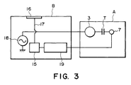
- Figure 3 is a diagram of an example of a toner amount measuring circuit in accordance with the present invention.
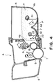
- Figure 4 is a drawing for showing the general structure of the process cartridge in the second embodiment of the present invention.
- Figure 5 is a drawing for depicting the essential portion of the process cartridge in the third embodiment of the present invention.
- Figure 6 is a drawing of a process cartridge comparable to the process cartridge illustrated in Figure 5.
- Figure 7 is a drawing for depicting a method for displaying the developer amount.
- Figure 8 is a drawing for depicting another method for displaying the developer amount.
- the process cartridge A in this embodiment integrally comprises: a photosensitive drum 1 as an electrophotographic photosensitive member; a charging means 2 for uniformly charging the peripheral surface of the photosensitive drum 1; a developing apparatus which comprises a development roller 3 as a developer bearing member placed in a manner to squarely oppose the photosensitive drum 1, and a developer containing portion 4b (developer storing portion; cartridge frame) which is located next to the development roller 3, and is formed of resinous material such as polystyrene; and a cleaning means holding portion 5 which contains a cleaning member 5.
- the developer holding portion 4b and cleaning means holding portion 5 are joined together to make up the frame of the process cartridge.
- the cartridge frame is formed of resinous material such as high impact styrene.
- an image is formed in the following manner.
- the photosensitive drum 1 is uniformly charged by the charging means 2, and the uniformly charged peripheral surface of the photosensitive drum 1 is exposed to the laser beam L projected in a scanning manner.
- an electrostatic latent image in accordance with image information is formed.
- This electrostatic latent image is developed into a visual image (developer image) by the development roller 3; the developer within the developer holding portion 4b is adhered to the peripheral surface of the photosensitive drum 1 by the development roller 3 in a manner to reflect the electrostatic latent image.
- the developer employed in this embodiment is electrically nonconductive, single component developer.
- the developer image on the photosensitive drum 1 is transferred by the transferring means 12, onto a sheet P of recording medium which has been fed out of a sheet cassette 13 and has been conveyed to the transferring means 12. Then, the recording medium sheet P is conveyed to a fixing means 14, in which the developer image is fixed to the recording medium sheet P. Thereafter, the recording medium sheet P is discharged out of the apparatus main assembly.
- the developer T within the developer holding portion 4b must be supplied to the development roller 3 through the opening 4a of the developer holding portion 4b (portion outlined by a dotted line in Figure 1).
- the opening 4a is sealed with an unillustrated sealing member. Therefore, a user must mount the process cartridge A into the apparatus main assembly after exposing the opening 4a by removing the sealing member.
- the developer holding portion 4b is wide, and therefore, two developer forwarding means 21 and 22 as developer conveying means are provided for supplying the developer within the developer holding portion 4b, to the development roller 3.
- the developer forwarding means 21 and 22 comprise rotational shafts 21a and 22a, and sheets 21b and 22b, respectively, which are formed of resinous material such as polyether resin or polyphenyl-sulfide resin.
- the sheets 21b and 22b are flexible.
- the developer holding portion 4b is shaped so that its bottom wall conforms to the shapes of the sweeping areas of the developer forwarding means 21 and 22.
- the developer T in the developer holding portion 4b can be sent to the developer roller 3 by the toner forwarding means 21 and 22 without being left at the bottom of the developer holding portion 4b.
- the development roller 3 is a nonmagnetic, metallic cylinder, and is rotationally placed in parallel to the photosensitive drum 1, with the provision of a predetermined distance between the peripheral surfaces of the photosensitive drum 1 and development roller 3.
- a magnet 3a is stationarily fixed.
- the peripheral surface of the development roller 3 is in contact with a regulating blade 8, as a developer regulating member, which is formed of urethane rubber and is fixed to a metallic supporting member 9.
- the developer T After being sent to the development roller 3 from the developer holding portion 4b, the developer T is adhered to the peripheral surface of the development roller 3 by being attracted by the magnetic force from the magnet 3a within the development roller 3. Then, as the development roller 3 is rotated, the developer T on the peripheral surface of the development roller 3 is carried to the adjacencies of the photosensitive drum 1.
- the amount of the developer T adhering to the development roller 3 is regulated by the blade 8 to a predetermined amount.
- a certain portion of the developer T adhering to the peripheral surface of the development roller 3 transfers onto the photosensitive drum 1 in response to the difference in potential level between the electrostatic latent image on the photosensitive drum 1, and the development roller 3, in the area in which the distance between the peripheral surfaces of the photosensitive drum 1 and development roller 3 is smallest, whereas the rest of the developer T adhering to the peripheral surface of the development roller 3 remains on the peripheral surface of the development roller 3.
- an AC bias with predetermined frequency and amplitude, and a variable DC bias are applied to the development roller 3.
- Figure 3 schematically shows a method for measuring the amount of the developer with the use of a developer amount detecting member 7, that is, the remaining developer amount detecting means in this embodiment.
- the AC bias is applied to the development roller 3 from a power source 18 provided on the apparatus main assembly side.
- electrical current the value of which corresponds to the electrostatic capacity between the development roller 3 and developer amount detecting member 7, flows between the two.
- This electrostatic capacity changes in response to the change in the amount of the developer T.
- the amount of the developer T between the development roller 3 and developer amount detecting member 7 can be continuously known by measuring the value of the electrical current which flows from the developer amount detecting member 7, with the use of a current detecting means 9.
- the developer amount detecting member 7 is formed of metallic material, for example, iron, aluminum, phosphor bronze, and the like. It is approximately the same in length as the development roller 3, and extends in the longitudinal direction of the development roller 3.
- the power source 18 for the bias to be applied to the development roller 3, the current measuring means 19 for measuring the current which flows to the developer amount detecting member 7, a converting means 15 for converting the detected current value into the developer amount, a displaying means for displaying the developer amount, a transmitting means 17 for transmitting the developer amount to the displaying means 16, and the like, are placed in the apparatus main assembly B.
- the printer main assembly B and process cartridge A are electrically connected to each other through the corresponding electrical contacts.
- the developer amount detecting member 7 that is, a piece of metallic plate or foil, is attached to the internal surface of the bottom wall of the developer holding portion 4b (cartridge frame), across the portion below the developer forwarding means 22, that is, the developer forwarding means closer to the development roller 3 of the two developer forwarding means 21 and 22. Further, the developer forwarding means 22 is placed between the development roller 3 and developer amount detecting member 7. This positioning of the developer detecting member 7 does not make it possible to measure the change in the developer amount within the sweeping range of the developer forwarding means 21.
- the amount of the developer on the development roller 3 falls below 20 g, it becomes impossible to form a satisfactory image.
- the developer forwarding means 22 which operates as described above, by the time the amount of the developer on the development roller 3 reduces to 20 g, there will be no developer, except for the developer on the development roller 3. Therefore, if the measured amount of the developer on the development roller 3 is 30 g, it is evident that the on-going image forming operation can be continued for a duration equivalent to 10 g of the developer, or the difference between 30 g and 20g.
- the amount of the developer which remains in the bottom portion of the developer holding portion 4b varies depending upon the operating environment, and therefore, a developer amount, below which a satisfactory image cannot be formed, is not definite. In other words, even if it is detected that the amount of the remaining developer is 25 g, it is still impossible to predict how long the current image forming operation can be continued.
- the developer forwarding means 22 is formed of only resinous material; in other words, no metallic material is used. This is due to the fact that if a substance, besides the developer, the amount of which affects the electrostatic capacity, is between the development roller 3 and developer amount detecting member 7, the developer amount cannot be accurately detected.
- the number of developer forwarding means is two.
- the present invention is also effectively applicable to an image forming apparatus with three or more developer forwarding means.
- the electrostatic capacity between the development roller 3 and developer amount detecting member 7 is measured immediately after the mounting of a process cartridge into the main assembly of an image forming apparatus.
- the developer amount detecting member 7 is placed outside the developer holding portion 4b, and in addition, the area of the exterior of the developer holding portion 4b, to which the developer amount detecting member 7 is attached, is covered with a cover 23 as shown in Figure 4.
- the developer holding portion 4b is formed of resin, and therefore, only thing that makes the electrostatic capacity between the development roller 3 and developer amount detecting member 7 in this embodiment different from that in the first embodiment is the increased distance between the development roller 3 and developer amount detecting member 7, which is greater by the thickness of the developer holding portion 4b than that in the first embodiment. Therefore, whether the developer amount detecting member 7 is within or outside the developer holding portion 4b, the developer amount in the developer holding portion 4b can be measured with the same continuity and accuracy as that in the first embodiment.
- the placement of the developer amount detecting member 7 outside the developer holding portion 4b in this embodiment makes it possible to place the entire wiring for transmitting electrical signals from the developer amount detecting member 7 to the contact of the printer main assembly B, on the exterior surface of the developer holding portion 4b.
- the signals outputted from the developer amount detecting member 7 are sent to the printer main assembly B through the contacts. For this reason, the wiring must be placed from the developer amount detecting member 7 to the contact on the exterior of the process cartridge A. If the developer amount detecting member 7 is within the developer holding portion 4b as in the first embodiment, the wiring from the developer amount detecting member 7 to the contact on the exterior of the process cartridge A must be put through the hole in the wall of the developer holding portion 4b.
- the placement of the developer amount detecting member 7 outside the developer holding portion 4b as in this embodiment makes it unnecessary to make a hole through the wall of the developer holding portion 4b.
- the cover 23 formed of resin is placed to cover the adjacencies of the exterior of the developer holding portion 4b and a part of the developing means frame portion, from the area corresponding to the position of the developer amount detecting member 7 to the area corresponding to the position of the development roller 3, as shown in Figure 4.
- this cover 23 which is placed in a manner to cover the adjacencies of the exterior of the developer holding portion 4b and a part of the developing means frame portion, from the area correspondent to the position of the development roller 3 to the area corresponding to the position of the developer amount detecting member 7, it is possible to prevent the problem that the accuracy with which the developer amount is measured is reduced by the adhesion of the foreign substances such as dust to the developer amount detecting member 7.
- the placement of the developer amount detecting member 7 outside the developer holding portion 4b as in this embodiment simplifies the process cartridge structure. Further, the provision of the cover as in this embodiment makes it possible to prevent the reduction in the developer amount measurement accuracy, without increasing the process cartridge size and/or the provision of an apparatus for removing the foreign substances which adhere to the developer amount detecting member 7.
- the developer amount detecting apparatus is structured so that the development roller 3 and a metallic supporting member 9 for supporting the toner regulating member 8 are made the same in potential level by an appropriate means, and the developer amount is determined from a combination of the measured electrostatic capacities between the development roller 3 and developer amount detecting member 7, and between the metallic supporting member 9 and developer amount detecting member 7.
- This structure is characterized by the positional relationships among the development roller 3, developer amount detecting member 7, and metallic supporting member 9.
- the region in which the change in the electrostatic capacity between the developer amount detecting member 7 and development roller 3 can be measured is the region sandwiched between a line L3 connecting the top end of the developer amount detecting member 7 and the highest point on the development roller 3, a line L4 connecting the bottom end of the developer amount detecting member 7 and the lowest point on the development roller 3, whereas the region in which the change in the electrostatic capacity between the developer amount detecting member 7 and metallic supporting member 9 can be measured is the region sandwiched between a line L1 connecting the top end of the developer amount detecting member 7 and the top end of the metallic supporting member 9, and a line L2 connecting the bottom end of the developer amount detecting member 7 and the bottom end of the metallic supporting member 9.
- the space S can be eliminated by extending the developer amount detecting member 7 by an appropriate length from its left end toward the development roller 3 following the line L4. With this arrangement, the developer amount within the region sandwiched between the lines L1 and L4 can be accurately measured.
- the developer amount detecting member 7 is placed so that no gap is created between the development roller 3 and metallic supporting member 9, as seen from the position of the developer amount detecting member 7. With this arrangement, no region in which accurate measurement of the development amount is impossible is created, and therefore, the developer amount can be accurately measured. Further, since the development roller 3 and metallic supporting member 9 are equal in potential level, the electrostatic capacity between the developer amount detecting member 7 and the combination of the development roller 3 and metallic supporting member 9 is greater than the electrostatic capacity measured in the preceding embodiments, increasing thereby the developer amount detection accuracy.
- the information detected by the above described developer amount detecting member 7 may be displayed on the monitor of the personal computer of the user of the image forming apparatus as shown in Figure 7.
- the developer amount is reported to the user as a point on a gauge 42 indicated by a hand 41, the movement of which is proportional to the developer amount.
- a display comprising a plurality of LEDs or the like may be directly placed on the main assembly of an electrophotographic image forming apparatus, so that the developer amount can be indicated by turning on or off a particular LED, among the plurality of the LEDs 43, which corresponds to the detected developer amount.
- the present invention does not limit the selection of the developer amount detection range to only a full range, that is, from the point at which the developer amount is 100% (developer holding portion 4b is full) to the point at which the developer amount is 0% (developer holding portion is empty).
- the range in which the developer amount is detected may be such a range in which the developer amount is from 30% down to 0% of the full amount.
- 0% does not mean that the developer has been completely consumed; it also includes such a condition that the amount of the developer in the developer holding portion 4b has decreased to a level below which it is impossible to produce an image with a predetermined level of quality.
- the remaining amount of the developer can be detected substantially real time.
Landscapes
- Physics & Mathematics (AREA)
- General Physics & Mathematics (AREA)
- Dry Development In Electrophotography (AREA)
- Electrophotography Configuration And Component (AREA)
- Developing For Electrophotography (AREA)
- Control Or Security For Electrophotography (AREA)
Abstract
Description
Claims (17)
- A process cartridge detachably mountable to a main assembly of an electrophotographic image forming apparatus, comprising:a cartridge frame;an electrophotographic photosensitive member;a developer accommodating portion for accommodating a developer;a developing member for developing an electrostatic latent image formed on said electrophotographic photosensitive member with the developer;a developer feeding member for feeding the developer accommodated in said developer accommodating portion toward said developing member; anda developer amount detecting member, disposed along a movement path of the developer from said developer accommodating portion toward said developing member, for generating an electric signal for permitting the main assembly to detect substantially real time a remaining amount of the developer in the process cartridge, wherein said developer amount detecting member is disposed at and along an arcuate portion which is provided outside said cartridge frame along a path of rotational motion of said developer feeding member.
- A process cartridge according to Claim 1, wherein said developer amount detecting member generates the electric signal corresponding to an electrostatic capacity between said developing member in the form of a developing roller and itself when a developing bias is applied to said developing roller from the main assembly of apparatus.
- A process cartridge according to Claim 2, wherein said developer feeding member comprises non-metal material, and said developer amount detecting member comprises metal material.
- A process cartridge according to Claim 1, 2 or 3, wherein said developer amount detecting member is provided on an inner surface of said arcuate portion, and said developer feeding member starts to slide on a surface of said developer amount detecting member when the remaining amount of the developer in said process cartridge reduces.
- A process cartridge according to Claim 1, 2 or 3, wherein said developer amount detecting member is provided on an outer surface of said arcuate portion, and said developer feeding member starts to slide on an inner surface of the arcuate portion when the remaining amount of the developer in said process cartridge reduces.
- A process cartridge according to Claim 5, wherein said developer amount detecting member provided on the outer surface of the arcuate portion is covered with a non-metal cover disposed on an outer surface outside said cartridge frame so as to bridge over a recess of said cartridge frame.
- A process cartridge detachably mountable to a main assembly of an electrophotographic image forming apparatus, comprising:a cartridge frame;an electrophotographic photosensitive drum;a developer accommodating portion for accommodating a developer;a developing roller for developing an electrostatic latent image formed on said electrophotographic photosensitive member with the developer;a non-metal developer feeding member for feeding the developer accommodation in said developer accommodating portion toward said developing roller;a developer amount detecting member of metal material, disposed along a movement path of the developer from said developer accommodating portion toward said developing member, for generating an electric signal for permitting the main assembly to detect substantially real time a remaining amount of the developer in the process cartridge, wherein said developer amount detecting member is disposed at and along an arcuate portion which is provided outside said cartridge frame along a path of rotational motion of said developer feeding member, and wherein said developer feeding member starts to slide on a surface of said arcuate portion when the remaining amount of the developer in said process cartridge reduces, and wherein said developer amount detecting member generates the electric signal corresponding to an electrostatic capacity between said developing member in the form of a developing roller and itself when a developing bias is applied to said developing roller from the main assembly of apparatus.
- A process cartridge according to Claim 7, wherein said developer amount detecting member provided on the outer surface of the arcuate portion is covered with a non-metal cover disposed on an outer surface outside said cartridge frame so as to bridge over a recess of said cartridge frame.
- An electrophotographic image forming apparatus for forming an image on a recording material, wherein a process cartridge is detachably mountable to said image forming apparatus, said apparatus comprising:(a) a mounting means for detachably mounting a process cartridge, said process cartridge including;an electrophotographic photosensitive member;a developer accommodating portion for accommodating a developer;a developing member for developing an electrostatic latent image formed on said electrophotographic photosensitive member with the developer;a developer feeding member for feeding the developer accommodated in said developer accommodating portion toward said developing member; anda developer amount detecting member, disposed along a movement path of the developer from said developer accommodating portion toward said developing member, for generating an electric signal for permitting the main assembly to detect substantially real time a remaining amount of the developer in the process cartridge, wherein said developer amount detecting member is disposed at and along an arcuate portion which is provided outside said cartridge frame along a path of rotational motion of said developer feeding member; and(b) detecting means for detecting the remaining amount of the developer in said process cartridge in accordance with the electric signal from said developer amount detecting member.
- An electrophotographic image forming apparatus for forming an image on a recording material, wherein a process cartridge is detachably mountable to said image forming apparatus, said apparatus comprising:(a) a mounting means for detachably mounting a process cartridge, said process cartridge including;an electrophotographic photosensitive member;a developer accommodating portion for accommodating a developer;a developing roller for developing an electrostatic latent image formed on said electrophotographic photosensitive member with the developer;a non-metal developer feeding member for feeding the developer accommodation in said developer accommodating portion toward said developing roller;a developer amount detecting member of metal material, disposed along a movement path of the developer from said developer accommodating portion toward said developing member, for generating an electric signal for permitting the main assembly to detect substantially real time a remaining amount of the developer in the process cartridge, wherein saiddeveloper amount detecting member is disposed at and along an arcuate portion which is provided outside said cartridge frame along a path of rotational motion of said developer feeding member, and wherein said developer feeding member starts to slide on a surface of said arcuate portion when the remaining amount of the developer in said process cartridge reduces, and wherein said developer amount detecting member generates the electric signal corresponding to an electrostatic capacity between said developing member in the form of a developing roller and itself when a developing bias is applied to said developing roller from the main assembly of apparatus; and(b) detecting means for detecting the remaining amount of the developer in said process cartridge in accordance with the electric signal from said developer amount detecting member.
- An apparatus according to Claim 9 or 10, further comprising a display portion for displaying substantially real time a remaining amount of the developer in said process cartridge, detected by said detecting means.
- An apparatus according to Claim 9 or 10, wherein the remaining amount of the developer in said process cartridge, detected by said detecting means is displayed substantially gradual on a display of a computer.
- A process cartridge detachably mountable to a main assembly of an electrophotographic image forming apparatus, the cartridge comprising:a cartridge frame;an electrophotograhpic photosensitive member (1);a developer accommodating portion (4) for accommodating a developer;a developing member (3) for developing an electrostatic latent image formed on said electrophotographic photosensitive member (1) using the developer;a developer feeding member (22) for feeding the developer accommodated in said developer accommodating portion (4) toward said developing member (3), wherein said developer feeding member (22) is sweepingly engageable with a part of the internal surface of a wall (4c) of the developer accommodating portion (4); anda developer amount detecting member (7) positioned along a movement path of the developer from said developer accommodating portion (4) toward said developing member (3), for generating an electrical signal representative of a remaining amount of the developer in the cartridge, wherein said developer amount detecting member (7) is disposed on said wall (4c) of the developer accommodating portion (4) at said area engageable by said developer feeding member (22).
- A process cartridge according to claim 13, wherein said developer amount detecting member (7) is mounted on an inside surface of said wall (4c) within said developer accommodating portion (4).
- A process cartridge according to claim 13, wherein said developer amount detecting member (7) is mounted on an outside surface of said wall (4c), outside said developer accommodating portion (4).
- A process cartridge according to claim 15, wherein a cover member (23) is provided over said developer amount detecting member (7).
- A process cartridge according to any of claims 13 to 16, wherein said electrical signal corresponds to an electrostatic capacity between said developing member (3) and said developer amount detecting member (7).
Applications Claiming Priority (4)
| Application Number | Priority Date | Filing Date | Title |
|---|---|---|---|
| JP2000037165 | 2000-02-15 | ||
| JP2000037165 | 2000-02-15 | ||
| JP2001025720 | 2001-02-01 | ||
| JP2001025720A JP3715897B2 (en) | 2000-02-15 | 2001-02-01 | Process cartridge and electrophotographic image forming apparatus |
Publications (3)
| Publication Number | Publication Date |
|---|---|
| EP1126330A2 true EP1126330A2 (en) | 2001-08-22 |
| EP1126330A3 EP1126330A3 (en) | 2005-08-03 |
| EP1126330B1 EP1126330B1 (en) | 2008-12-31 |
Family
ID=26585409
Family Applications (1)
| Application Number | Title | Priority Date | Filing Date |
|---|---|---|---|
| EP01301316A Expired - Lifetime EP1126330B1 (en) | 2000-02-15 | 2001-02-15 | Process cartridge and image forming apparatus |
Country Status (6)
| Country | Link |
|---|---|
| US (1) | US6477336B2 (en) |
| EP (1) | EP1126330B1 (en) |
| JP (1) | JP3715897B2 (en) |
| KR (1) | KR100392994B1 (en) |
| CN (1) | CN1267794C (en) |
| DE (1) | DE60137157D1 (en) |
Cited By (1)
| Publication number | Priority date | Publication date | Assignee | Title |
|---|---|---|---|---|
| EP1355202A3 (en) * | 2002-04-17 | 2004-06-09 | Canon Kabushiki Kaisha | Developing apparatus |
Families Citing this family (14)
| Publication number | Priority date | Publication date | Assignee | Title |
|---|---|---|---|---|
| US6785479B2 (en) | 2001-12-28 | 2004-08-31 | Canon Kabushiki Kaisha | Image forming apparatus having a control section for detecting an amount of developer and an amount detection method of developer of image forming apparatus |
| EP1533658B1 (en) * | 2002-06-28 | 2013-09-04 | Canon Kabushiki Kaisha | Photosensitive body for electrophotography, process cartridge, and electrophotographic apparatus |
| US6962399B2 (en) | 2002-12-30 | 2005-11-08 | Lexmark International, Inc. | Method of warning a user of end of life of a consumable for an ink jet printer |
| JP3971330B2 (en) * | 2003-03-19 | 2007-09-05 | シャープ株式会社 | Toner remaining amount detection device, toner cartridge, and image forming apparatus |
| USD537110S1 (en) * | 2004-07-01 | 2007-02-20 | Seiko Epson Corporation | Photoconductor cartridge |
| JP4630166B2 (en) * | 2005-09-27 | 2011-02-09 | 株式会社沖データ | Developer accommodating device, developing device, and image forming apparatus |
| JP4424330B2 (en) | 2006-06-02 | 2010-03-03 | 富士ゼロックス株式会社 | Powder feeder, method for setting powder filling amount in powder feeder, and method for setting powder filling amount in regenerated powder feeder |
| JP4479693B2 (en) | 2006-06-02 | 2010-06-09 | 富士ゼロックス株式会社 | Powder feeder, powder feeder manufacturing method, and powder feeder regeneration method |
| CN101673073B (en) * | 2008-09-11 | 2013-04-17 | 株式会社理光 | Developer residue detection and developing equipment, processing unit and imaging equipment |
| CN101986213B (en) * | 2010-12-09 | 2012-07-25 | 珠海艾派克微电子有限公司 | Developer capacity detecting unit for imaging device and imaging device |
| US9791826B2 (en) * | 2013-07-12 | 2017-10-17 | Canon Kabushiki Kaisha | Developing apparatus having a frame portion with varied thickness, and process cartridge thereof |
| JP5868456B2 (en) * | 2013-07-12 | 2016-02-24 | キヤノン株式会社 | Developer container, developing device, process cartridge, and image forming apparatus |
| US10466617B2 (en) * | 2017-12-19 | 2019-11-05 | Lexmark International, Inc. | Capacitive toner level sensor |
| JP7205361B2 (en) * | 2019-04-17 | 2023-01-17 | 株式会社リコー | Toner amount detection device, toner amount detection method, toner amount detection program |
Family Cites Families (22)
| Publication number | Priority date | Publication date | Assignee | Title |
|---|---|---|---|---|
| JPS54111355A (en) * | 1978-02-20 | 1979-08-31 | Ricoh Co Ltd | Residual quantity detector of toner |
| JPS59184375A (en) * | 1983-04-04 | 1984-10-19 | Canon Inc | Image forming method |
| JPH02144582A (en) * | 1988-11-26 | 1990-06-04 | Mita Ind Co Ltd | Developing device |
| JPH02197881A (en) * | 1989-01-27 | 1990-08-06 | Canon Inc | Developer detection device |
| JPH02216167A (en) * | 1989-02-17 | 1990-08-29 | Ricoh Co Ltd | developing device |
| JPH02251874A (en) * | 1989-03-27 | 1990-10-09 | Fuji Xerox Co Ltd | Device for detecting amount of toner in container |
| US5095335A (en) | 1989-09-19 | 1992-03-10 | Canon Kabushiki Kaisha | Copier with retractable charging unit to prevent damage to drum when removing process cartridge |
| EP0443461B1 (en) | 1990-02-17 | 1994-08-24 | Canon Kabushiki Kaisha | Process cartridge and image forming apparatus usable with same |
| JPH04177381A (en) * | 1990-11-13 | 1992-06-24 | Fujitsu Ltd | Toner quantity detecting method |
| JPH04355477A (en) * | 1991-05-31 | 1992-12-09 | Canon Inc | Image forming device |
| JP3255175B2 (en) | 1991-10-03 | 2002-02-12 | キヤノン株式会社 | Toner presence detection device |
| JPH0651631A (en) * | 1992-07-29 | 1994-02-25 | Mita Ind Co Ltd | Developing device |
| JPH07199636A (en) * | 1993-12-28 | 1995-08-04 | Fujitsu Ltd | Toner level detector |
| KR0131958B1 (en) * | 1994-11-10 | 1998-10-01 | 김광호 | Process Cartridge Replacement Method and Device |
| JPH09101671A (en) * | 1995-10-05 | 1997-04-15 | Mita Ind Co Ltd | Electrostatic latent image developing device |
| JP3445040B2 (en) * | 1995-10-09 | 2003-09-08 | キヤノン株式会社 | Image forming device |
| DE69627803T2 (en) | 1995-12-26 | 2004-04-01 | Canon K.K. | Lifetime display device of a charged image carrier part, display method therefor, and image generation device |
| JPH09211960A (en) * | 1996-01-29 | 1997-08-15 | Canon Inc | Process cartridge and image forming apparatus |
| KR0185093B1 (en) * | 1996-06-03 | 1999-04-15 | 유기범 | Toner remaining amount display method and apparatus |
| JPH10301385A (en) * | 1997-02-28 | 1998-11-13 | Brother Ind Ltd | Apparatus for detecting remaining amount of toner in image forming apparatus |
| KR19990074822A (en) * | 1998-03-14 | 1999-10-05 | 윤종용 | Residual Toner Display Method in Image Forming Apparatus and Its Display Apparatus |
| JP2000029372A (en) * | 1998-07-14 | 2000-01-28 | Ricoh Co Ltd | Image forming device |
-
2001
- 2001-02-01 JP JP2001025720A patent/JP3715897B2/en not_active Expired - Fee Related
- 2001-02-12 US US09/780,419 patent/US6477336B2/en not_active Expired - Lifetime
- 2001-02-15 CN CNB01117806XA patent/CN1267794C/en not_active Expired - Fee Related
- 2001-02-15 EP EP01301316A patent/EP1126330B1/en not_active Expired - Lifetime
- 2001-02-15 KR KR10-2001-0007401A patent/KR100392994B1/en not_active Expired - Fee Related
- 2001-02-15 DE DE60137157T patent/DE60137157D1/en not_active Expired - Lifetime
Cited By (2)
| Publication number | Priority date | Publication date | Assignee | Title |
|---|---|---|---|---|
| EP1355202A3 (en) * | 2002-04-17 | 2004-06-09 | Canon Kabushiki Kaisha | Developing apparatus |
| US6839535B2 (en) | 2002-04-17 | 2005-01-04 | Canon Kabushiki Kaisha | Developing apparatus |
Also Published As
| Publication number | Publication date |
|---|---|
| CN1321920A (en) | 2001-11-14 |
| US20010021314A1 (en) | 2001-09-13 |
| KR20010102833A (en) | 2001-11-16 |
| US6477336B2 (en) | 2002-11-05 |
| JP3715897B2 (en) | 2005-11-16 |
| CN1267794C (en) | 2006-08-02 |
| EP1126330A3 (en) | 2005-08-03 |
| JP2001305847A (en) | 2001-11-02 |
| DE60137157D1 (en) | 2009-02-12 |
| EP1126330B1 (en) | 2008-12-31 |
| KR100392994B1 (en) | 2003-07-31 |
Similar Documents
| Publication | Publication Date | Title |
|---|---|---|
| US7095967B2 (en) | Image developing apparatus, process cartridge, electrophotographic image forming apparatus, and developing unit frame | |
| US6892035B2 (en) | Developing device, a process cartridge, and an electrophotographic image forming apparatus for detecting an amount of developer | |
| US6477336B2 (en) | Process cartridge and image forming apparatus having a developer amount detecting member | |
| US7532828B2 (en) | Image forming apparatus and developer remaining amount detecting method | |
| EP1117015B1 (en) | Process cartridge and image forming apparatus | |
| JP2001356655A (en) | Image carrier life detecting method, image forming apparatus and cartridge | |
| JP2000206774A (en) | Toner remaining amount detecting device, toner remaining amount detecting method, process cartridge, and electrophotographic image forming apparatus | |
| US6668141B2 (en) | Image forming apparatus, cartridge, image forming system, and a memory device for determining the amount of developer in a developer containing portion | |
| US6349184B2 (en) | Process cartridge with toner amount detector having different patterns according to fill amount | |
| JP3352076B2 (en) | Apparatus and method for measuring wear of photoconductor | |
| US6615001B2 (en) | Cartridge, image forming apparatus and method of controlling the image forming apparatus | |
| US6282384B1 (en) | Developing device, process cartridge and electrophotographic image forming apparatus | |
| US6275665B1 (en) | Developing device, process cartridge and electrophotographic image forming apparatus | |
| US6314250B1 (en) | Developing device, process cartridge and electrophotographic image forming apparatus with capacitance detector for detecting residual toner amount | |
| JP2000250380A (en) | Developing device, process cartridge, electrophotographic image forming device, and developing frame | |
| US6636706B2 (en) | Electrophotographic image forming apparatus | |
| JP3984759B2 (en) | Developing device, process cartridge, and electrophotographic image forming apparatus | |
| JP4724310B2 (en) | Developer amount detection system and image forming apparatus | |
| JP2025002168A (en) | Image-forming device, toner remaining amount detection device, and toner remaining amount detection method | |
| JP2000338763A (en) | Developing device, process cartridge, and electrophotographic image forming device | |
| JPH10260578A (en) | Developing device | |
| JP2002351206A (en) | Developing device and process cartridge | |
| JP2001194885A (en) | Developer remaining amount detecting device, developing device, process cartridge and electrophotographic image forming apparatus | |
| JP2001125378A (en) | Developing device, process cartridge, and electrophotographic image forming device | |
| JP2007108607A (en) | Image forming apparatus and developer remaining amount detecting method of the image forming apparatus |
Legal Events
| Date | Code | Title | Description |
|---|---|---|---|
| PUAI | Public reference made under article 153(3) epc to a published international application that has entered the european phase |
Free format text: ORIGINAL CODE: 0009012 |
|
| AK | Designated contracting states |
Kind code of ref document: A2 Designated state(s): AT BE CH CY DE DK ES FI FR GB GR IE IT LI LU MC NL PT SE TR |
|
| AX | Request for extension of the european patent |
Free format text: AL;LT;LV;MK;RO;SI |
|
| PUAL | Search report despatched |
Free format text: ORIGINAL CODE: 0009013 |
|
| AK | Designated contracting states |
Kind code of ref document: A3 Designated state(s): AT BE CH CY DE DK ES FI FR GB GR IE IT LI LU MC NL PT SE TR |
|
| AX | Request for extension of the european patent |
Extension state: AL LT LV MK RO SI |
|
| 17P | Request for examination filed |
Effective date: 20060203 |
|
| AKX | Designation fees paid |
Designated state(s): DE FR GB IT |
|
| 17Q | First examination report despatched |
Effective date: 20060818 |
|
| GRAP | Despatch of communication of intention to grant a patent |
Free format text: ORIGINAL CODE: EPIDOSNIGR1 |
|
| GRAS | Grant fee paid |
Free format text: ORIGINAL CODE: EPIDOSNIGR3 |
|
| GRAA | (expected) grant |
Free format text: ORIGINAL CODE: 0009210 |
|
| AK | Designated contracting states |
Kind code of ref document: B1 Designated state(s): DE FR GB IT |
|
| REG | Reference to a national code |
Ref country code: GB Ref legal event code: FG4D |
|
| REF | Corresponds to: |
Ref document number: 60137157 Country of ref document: DE Date of ref document: 20090212 Kind code of ref document: P |
|
| PLBE | No opposition filed within time limit |
Free format text: ORIGINAL CODE: 0009261 |
|
| STAA | Information on the status of an ep patent application or granted ep patent |
Free format text: STATUS: NO OPPOSITION FILED WITHIN TIME LIMIT |
|
| REG | Reference to a national code |
Ref country code: FR Ref legal event code: ST Effective date: 20091030 |
|
| 26N | No opposition filed |
Effective date: 20091001 |
|
| PG25 | Lapsed in a contracting state [announced via postgrant information from national office to epo] |
Ref country code: FR Free format text: LAPSE BECAUSE OF NON-PAYMENT OF DUE FEES Effective date: 20090302 |
|
| PG25 | Lapsed in a contracting state [announced via postgrant information from national office to epo] |
Ref country code: IT Free format text: LAPSE BECAUSE OF FAILURE TO SUBMIT A TRANSLATION OF THE DESCRIPTION OR TO PAY THE FEE WITHIN THE PRESCRIBED TIME-LIMIT Effective date: 20081231 |
|
| PGFP | Annual fee paid to national office [announced via postgrant information from national office to epo] |
Ref country code: DE Payment date: 20170228 Year of fee payment: 17 |
|
| PGFP | Annual fee paid to national office [announced via postgrant information from national office to epo] |
Ref country code: GB Payment date: 20170227 Year of fee payment: 17 |
|
| REG | Reference to a national code |
Ref country code: DE Ref legal event code: R119 Ref document number: 60137157 Country of ref document: DE |
|
| GBPC | Gb: european patent ceased through non-payment of renewal fee |
Effective date: 20180215 |
|
| PG25 | Lapsed in a contracting state [announced via postgrant information from national office to epo] |
Ref country code: DE Free format text: LAPSE BECAUSE OF NON-PAYMENT OF DUE FEES Effective date: 20180901 |
|
| PG25 | Lapsed in a contracting state [announced via postgrant information from national office to epo] |
Ref country code: GB Free format text: LAPSE BECAUSE OF NON-PAYMENT OF DUE FEES Effective date: 20180215 |