EP1126302A2 - Method of designing collimator array device and collimator array device manufactured thereby - Google Patents
Method of designing collimator array device and collimator array device manufactured thereby Download PDFInfo
- Publication number
- EP1126302A2 EP1126302A2 EP01301362A EP01301362A EP1126302A2 EP 1126302 A2 EP1126302 A2 EP 1126302A2 EP 01301362 A EP01301362 A EP 01301362A EP 01301362 A EP01301362 A EP 01301362A EP 1126302 A2 EP1126302 A2 EP 1126302A2
- Authority
- EP
- European Patent Office
- Prior art keywords
- emitting side
- optical
- laser beam
- receiving side
- side lens
- Prior art date
- Legal status (The legal status is an assumption and is not a legal conclusion. Google has not performed a legal analysis and makes no representation as to the accuracy of the status listed.)
- Withdrawn
Links
Images



Classifications
-
- G—PHYSICS
- G02—OPTICS
- G02B—OPTICAL ELEMENTS, SYSTEMS OR APPARATUS
- G02B6/00—Light guides; Structural details of arrangements comprising light guides and other optical elements, e.g. couplings
- G02B6/24—Coupling light guides
- G02B6/26—Optical coupling means
- G02B6/35—Optical coupling means having switching means
- G02B6/3564—Mechanical details of the actuation mechanism associated with the moving element or mounting mechanism details
- G02B6/3582—Housing means or package or arranging details of the switching elements, e.g. for thermal isolation
-
- G—PHYSICS
- G02—OPTICS
- G02B—OPTICAL ELEMENTS, SYSTEMS OR APPARATUS
- G02B6/00—Light guides; Structural details of arrangements comprising light guides and other optical elements, e.g. couplings
- G02B6/24—Coupling light guides
- G02B6/26—Optical coupling means
- G02B6/35—Optical coupling means having switching means
- G02B6/351—Optical coupling means having switching means involving stationary waveguides with moving interposed optical elements
- G02B6/3512—Optical coupling means having switching means involving stationary waveguides with moving interposed optical elements the optical element being reflective, e.g. mirror
-
- G—PHYSICS
- G02—OPTICS
- G02B—OPTICAL ELEMENTS, SYSTEMS OR APPARATUS
- G02B6/00—Light guides; Structural details of arrangements comprising light guides and other optical elements, e.g. couplings
- G02B6/24—Coupling light guides
- G02B6/26—Optical coupling means
- G02B6/35—Optical coupling means having switching means
- G02B6/354—Switching arrangements, i.e. number of input/output ports and interconnection types
- G02B6/3544—2D constellations, i.e. with switching elements and switched beams located in a plane
- G02B6/3546—NxM switch, i.e. a regular array of switches elements of matrix type constellation
Definitions
- the present invention relates to a method of designing a collimator array device which is used as an optical path changing switch module, an optical demultiplexing filter module, or the like, in an optical communication system, and a collimator array device manufactured by the method.
- the above-mentioned module is obtained by combining a collimator array device and an optical switch array, an optical demultiplexing filter, or the like.
- the whole device is referred to as a collimator array device.
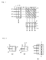
- FIGS. 1 and 2 A general collimator array device (four by four optical switch modules) is shown in FIGS. 1 and 2.
- reference mark 1 indicates an emitting side fiber array.
- Reference mark 2 indicates an emitting side planar microlens.
- Reference mark 3 indicates an optical switch array.
- Reference mark 4 indicates a receiving side microlens.
- Reference mark 5 indicates a receiving side fiber array.
- the emitting side fiber array 1 and the receiving side fiber array 5 are respectively formed by installing a plurality of single mode optical fibers la and 5a between two sheets of silicon substrates 6a and 6b.
- Lenses 2a and 4a having diameters of about 250 ⁇ m, are respectively formed in the emitting side planar microlens 2 and the receiving side microlens 4.
- Mirrors 3a are provided per a pixel in the optical switch array 3.
- Mirror 3a is made to reflect or transmit light by inserting the mirror of a minute size in the optical path or displacing therefrom, or by electrically varying the refractive index of the material for the front and the back of the reflection surface. Therefore, the channel can be changed between the emitting side fiber array 1 and the receiving side fiber array 5 by combining the reflection and the transmission of each of the mirrors 3a, arranged 4 by 4, of the optical switch array 3.
- the laser beam emitted from the end surface of the single mode optical fiber la installed in the emitting side fiber array 1 is collimated by the lens 2a formed in the emitting side planar microlens 2.
- the optical path of the collimated laser beam is deviated by the optical switch array 3, and thereafter, the laser beam is converged by the lens 4a formed in the receiving side microlens 4.
- the converged laser beam is made incident upon the single mode optical fiber 5a installed in the receiving side fiber array 5.
- the laser beam emitted from the optical fiber A1 is made incident upon the optical fiber B4, the laser beam emitted from the optical fiber A2 is made incident upon the optical fiber B2, the laser beam emitted from the optical fiber A3 is made incident upon the optical fiber B3, and the laser beam emitted from the optical fiber A4 is made incident upon the optical fiber B1.
- a laser beam is Gaussian beam the intensity of which is large in the center portion and small in the periphery portion.
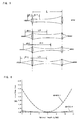
- the feature of Gaussian beam is shown in FIG. 3. While the light emitted from the emitting side optical fiber la side is collimated by the emitting side lens 2a, converged by the receiving side lens 4a, and made incident upon the receiving side optical fiber 5a, the collimated light is not parallel, i.e., it has a beam waist of 2W1 width in the intermediate portion. In addition, it does not converge upon one point (focal point).
- the end surface of the receiving side optical fiber 5a be adjusted to accurately coincide with the beam waist position of the laser beam emitted from the receiving side lens 4a and that the mode field diameter of the receiving side optical fiber 5a and the width 2W2 of the beam waist of the laser beam incident thereupon be adjusted to coincide (coupling).
- the beam waist of the laser beam emitted from the lens 2a be positioned at half of the distance between the emitting side lens 2a and the receiving side lens 4a, i.e., the optical length L.
- the distance dl between the end surface of the emitting side planar microlens and the beam waist be equal to L/2.
- the optical length L from the emitting side planar microlens through the receiving side planar microlens is varied. For example, in FIG.
- the optical length of the laser beam emitted from the optical fiber A1 and incident upon the optical fiber B4 is 11 mm (8 mm + 3 mm), which is the largest, and the optical length of the laser beam emitted from the optical fiber A4 and incident upon the optical fiber B1 is 5 mm (8mm - 3mm) which is the smallest.
- the standard value (8 mm) indicates the mean length in this case.
- the laser beam passing from the emitting side lens 2a through the receiving side lens 4a has a beam waist.
- the position of the beam waist is determined by the distance do between the end surface of the emitting side optical fiber la and the emitting side lens 2a. Therefore, if the optical length L is different from the condition shown in FIG. 3, i.e., the position of the receiving side lens 4a is shifted to the left side or the right side in FIG. 3, the position of the beam waist 2W2 of the laser beam emitted from the receiving side lens 4a is varied, the position of the beam waist 2W2 is shifted from the end surface of the receiving side optical fiber 5a, and thereby the insertion loss is increased.
- the linear expansivities thereof are also different. Therefore, in such a case, if thermal variation occurs, the core of the optical fiber is shifted from the center of the lens.
- an optical functional array module is manufactured by forming a collimator optical system comprised of a pair of fiber arrays and a pair of planar microlenses and inserting various optical functional elements into the collimated optical path, the optical length is shifted or varied with regards to the ideal value depending on the operation condition or the insertion position of the optical functional element, or the accuracy of fixing the components.
- the first purpose of the present invention at least in preferred embodiments is to provide an optimum designing method with regards to a collimator array optical system which is subject to the variation of the optical length.
- Another purpose of the present invention at least in preferred embodiments is to provide an optimum designing method with regards to an optical system using a general convergent lens.
- a method of designing a collimator array device in which a laser beam, having a feature of a Gaussian beam, emitted from an emitting side fiber array is collimated by an emitting side lens, the collimated laser beam is made incident upon an optical functional element and thereafter converged by a receiving side lens, and the converged laser beam is made incident upon a receiving side fiber array, comprising the steps of:
- a collimator array device in which a laser beam, having the feature of Gaussian beam, emitted from an emitting side fiber array is collimated by an emitting side lens, the collimated laser beam is made incident upon an optical functional element and thereafter converged by a receiving side lens, and the converged laser beam is made incident upon a receiving side fiber array, wherein the distance do between said emitting side fiber array and said emitting side lens is the smaller value of two values obtained based on a mean value La of the optical length L of the laser beam which passes from said emitting side lens through said receiving side lens.
- a method of designing a collimator array device having an optical functional element comprising the steps of: calculating a mean value La of the optical length L which is varied depending on the combination of an emitting side optical fiber and a receiving side optical fiber, and obtaining the distance do between the emitting side fiber array and an emitting side lens in which the distance dl from the emitting side lens through the beam waist of the laser beam collimated by the emitting side lens is equal to La/2.
- the emitting side lens and the receiving side lens are not limited to a planar microlens.
- a homogenous lens such as a spherical lens; an aspherical lens, or the like; a graded index lens such as a graded index in radical direction rod lens, a graded index in axis direction spherical lens, or the like; and a grating lens such as Fresnel lens or the like may be used.
- the optical functional element varies the optical length L of the laser beam depending on the operation condition thereof.
- an optical switch array or (an) optical demultiplexing filter(s) for changing the channel between the emitting side fiber array and the receiving side fiber array can be listed as examples of the optical functional element.
- one edge or two adjacent edges of the emitting side planar microlens and the receiving side planar microlens are fixed, can the emitting side planar microlens and the receiving side planar microlens can expand or shrink in the same direction with regards to the optical axis in a case where thermal variation occurs.
- the other portions are not fixed.
- junction structure between the emitting side optical fiber la and the emitting side planar microlens 2 can be improved as shown in FIGS. 2 (b) or 2 (c).
- the end surface of the emitting side optical fiber la and the end surface, contacting therewith, of the emitting side planar microlens 2 are polished to incline 2 to 10 degrees.
- the emitting side planar microlens 2 is comprised of two sheets of microlens array.
- NA numerical aperture
- each sheet of microlens arrays has a numerical aperture of 0.2
- two sheets of microlens arrays have a numerical aperture of about 0.4 in total.
- junction structure between an emitting side optical fiber and the emitting side planar microlens can be applied to the receiving side optical fiber and the receiving side planar microlens.
- the condition for obtaining the maximum efficiency in the optical system which is from the emitting side optical fiber la through the receiving side optical fiber 5a is that dl is equal to L/2.
- the width of the waist at the emitting side is designated by 2W0
- the width of the waist after passing the lens is designated by 2W1
- the focal length of the lens is designated by f
- the wavelength is designated by ⁇
- the distance between the waist at the emitting side and the lens is designated by do.
- the distance dl between the lens and the waist after passing therethrough is expressed by the following equations (1) and (2).
- FIG. 5 explains the relationship between the distance do and the distance dl shown in FIG. 4 in relation to the coupling condition. It turns out that the distance dl becomes larger as the distance d0 is gradually made larger from the smallest value (around 700 ⁇ m in this embodiment).
- the beam waist is positioned to the side of the emitting side planar microlens, and thereby an accurate coupling is not obtained.
- the beam waist is positioned to the side of the receiving side planar microlens, and thereby an accurate coupling is not obtained,either.
- no beam waist is formed at a receiving side fiber array the mode field diameter of which is the same as the emitting side fiber array i.e., 10.5 ⁇ m, or the width of the formed beam waist is larger or smaller than 10.5 ⁇ m, and thereby the coupling efficiency is decreased.
- the insertion loss (coupling rate ⁇ ) can be calculated using the following equation (3) after the width 2W2 of the waist at the receiving side fiber is obtained by applying the above-mentioned equation (2) to each of two planar microlenses.
- Equation 3 indicates the shift of the waist position from the end surface of the receiving side fiber in the direction of the optical axis. This is also obtained by applying the above-mentioned equation (1) two times. Further, xo indicates the shift amount of the beam waist in the transverse direction.
- the insertion loss which is obtained by adding the variation of the optical length L to the two conditions of the distance do between the waist at the emitting side and the lens, using equation 3, is shown in FIG. 6.
- FIG. 6 shows that the smaller one of the two conditions of the distance do is preferable for the present case.
- the optical length L is varied depending on the combination of the emitting side optical fiber and the receiving side optical fiber.
- Such a variation of the optical length L causes the shift of the beam waist position of the laser beam emitted from the end surface of the receiving side planar microlens. It is difficult to completely prevent such a shift because of the structure of a collimator array device.
- one edge of the emitting side planar microlens 2 and the receiving side planar microlens 4 is fixed with a supporting body 6.
- the other portions are not fixed so as to expand and shrink depending on the thermal variation.
- the linear expansivities thereof are also different. As a result, the center of the lens is shifted with regards to the optical axis.
- FIG. 9 is a graph showing the relationship between the direction of the shift of the emitting side microlens and the receiving side microlens and the insertion loss. If the emitting side microlens 2 and the receiving side microlens 4 are shifted in contrary directions with regards to the optical axis, as shown in FIG. 8(a), the beam waist of the laser beam emitted from the receiving side microlens 4 is greatly deviated from the end surface of the single mode optical fiber 5a of the receiving side fiber array 5. Therefore, one specific edge of the emitting side planar microlens 2 and the receiving side planar microlens 4 is fixed with a supporting body 6.
- one edge is pushed onto a rigid body and fixed by adhesion or fusion.
- the other edge is loosely supported with a soft adhesive of relatively low Young's modulus (not shown).
- two adjacent edges of the emitting side planar microlens 2 and the receiving side planar microlens 4 are fixed with a supporting body 6.
- the other potions are not fixed, so that it is possible to expand and shrink.
- an optical switch array is shown as an optical functional element.
- the present invention can be applied to a collimator array device in which anonther optical functional element for varying the optical length L is installed, for example, a demultiplexing filter or the like. It is not limited to an optical switch array.
- the planar microlens array according to the present invention is not limited to one in which microlenses are formed on one sheet of substrate as a unity. It is also possible to use a microlens array which is obtained by arranging, for example, ball lenses, graded index rod lenses, aspherical lenses, or the like, based on a substrate, a holder, a housing, or the like. In such a case, a designing method according to the present invention can be applied in the same way. Also, a method of fixing a microlens according to the present invention can be applied to a microlens array together with a substrate or a holder for arranging the microlens array.
- a planar microlens which is a convergent lens
- a homogenous lens such as a spherical lens; an aspherical lens, or the like; a graded index lens such as a graded index in radical direction rod lens, a graded index in axis direction spherical lens, or the like; and Fresnel lens or the like may be used.
- each lens is formed with an ion exchange or a wet etching via a photomask, and thereby the arranging position of each lens has high accuracy.
- a planar microlens is manufactured with one process such as an ion exchange or the like, and thereby the differences in the performance of the focal length, the spherical aberration, or the like, can be greatly reduced.
- a method of designing a collimator array device comprising the steps of: calculating a mean value La of the optical length L of the laser beam which passes from an emitting side lens (a planar microlens) through a receiving side lens (a planar microlens), obtaining two values of the distance d0 between an emitting side fiber array and an emitting side lens (a planar microlens) in which the distance from the emitting side lens (a planar microlens) through the beam waist of the laser beam collimated by the emitting side lens (a planar microlens) is equal to La/2, and selecting the smaller value.
- a fixing method of at least preferred embodiments of the present invention even if the materials for the fiber array and the planar microlens are different in a thermal expansion coefficient, it is possible to prevent the loss due to the shift with regards to the optical axis which is caused by the difference in a thermal expansion coefficient from increasing.
Landscapes
- Physics & Mathematics (AREA)
- General Physics & Mathematics (AREA)
- Optics & Photonics (AREA)
- Optical Couplings Of Light Guides (AREA)
- Mechanical Light Control Or Optical Switches (AREA)
Abstract
Description


Such a variation of the optical length L causes the shift of the beam waist position of the laser beam emitted from the end surface of the receiving side planar microlens. It is difficult to completely prevent such a shift because of the structure of a collimator array device.
Claims (12)
- A method of designing a collimator array device in which a laser beam, having a feature of a Gaussian beam, emitted from an emitting side fiber array (1) is collimated by an emitting side lens (2), the collimated laser beam is made incident upon an optical functional element (3) and thereafter converged by a receiving side lens (4), and the converged laser beam is made incident upon a receiving side fiber array (5), comprising the steps of:calculating a mean value La of the optical length L of the laser beam which passes from said emitting side lens through said receiving side lens;obtaining two values of the distance d0 between said emitting side fiber array and said emitting side lens in which the distance from said emitting side lens through the beam waist of the laser beam collimated by said emitting side lens is equal to La/2; andselecting the smaller value of said two obtained values.
- A method of designing a collimator array device according to claim 1, wherein said emitting side lens (2) and said receiving side lens (4) are planar microlenses.
- A method of designing a collimator array device according to claim 1 or claim 2, wherein said optical functional element (3) varies the optical length L of said laser beam depending on the operation condition thereof.
- A method of designing a collimator array device according to claim 1 or claim 2, wherein said optical functional element (3) is an optical switch array for changing the channel between said emitting side fiber array (1) and said receiving side fiber array (5).
- A method of designing a collimator array device according to claim 1 or claim 2, wherein said optical functional element (3) is a single optical demultiplexing filter or plural optical demultiplexing filters.
- A collimator array device in which a laser beam, having the feature of Gaussian beam, emitted from an emitting side fiber array (1) is collimated by an emitting side lens (2), the collimated laser beam is made incident upon an optical functional element (3) and thereafter converged by a receiving side lens (4), and the converged laser beam is made incident upon a receiving side fiber array (5), wherein the distance do between said emitting side fiber array and said emitting side lens is the smaller value of two values obtained based on a mean value La of the optical length L of the laser beam which passes from said emitting side lens through said receiving side lens.
- A collimator array device according to claim 6, wherein said emitting side lens (2) and said receiving side lens (4) are planar microlenses.
- A collimator array device according to claim 7, wherein one edge or two adjacent edges of said emitting side planar microlens (2) and the receiving side planar microlens (4) are fixed, so that said emitting side planar microlens and the receiving side planar microlens can expand or shrink in the same direction with regards to the optical axis in a case where thermal variation occurs, and the other portions are not fixed.
- A collimator array device according to claim 7, wherein an end surface of an emitting side optical fiber (la) of said emitting side fiber array (1) and the end surface, in contact therewith, of said emitting side planar microlens (2) are polished to incline 2 to 10 degrees from a plane perpendicular to the optical axis.
- A collimator array device according to claim 6 or claim 7, wherein said optical functional element (3) varies the optical length L of said laser beam depending on the operation condition thereof.
- A collimator array device according to claim 6 or claim 7, wherein said optical functional element (3) is an optical switch array for changing the channel between said emitting side fiber array and said receiving side fiber array (5).
- A collimator array device according to claim 6 or claim 7, wherein said optical functional element (3) is a single optical demultiplexing filter or plural optical demultiplexing filters.
Applications Claiming Priority (4)
| Application Number | Priority Date | Filing Date | Title |
|---|---|---|---|
| JP2000038952 | 2000-02-17 | ||
| JP2000038952 | 2000-02-17 | ||
| JP2001036764 | 2001-02-14 | ||
| JP2001036764A JP2001305376A (en) | 2000-02-17 | 2001-02-14 | Method for designing collimator array device and collimator array device manufactured by this method |
Publications (2)
| Publication Number | Publication Date |
|---|---|
| EP1126302A2 true EP1126302A2 (en) | 2001-08-22 |
| EP1126302A3 EP1126302A3 (en) | 2004-07-07 |
Family
ID=26585517
Family Applications (1)
| Application Number | Title | Priority Date | Filing Date |
|---|---|---|---|
| EP01301362A Withdrawn EP1126302A3 (en) | 2000-02-17 | 2001-02-16 | Method of designing collimator array device and collimator array device manufactured thereby |
Country Status (3)
| Country | Link |
|---|---|
| US (1) | US6912091B2 (en) |
| EP (1) | EP1126302A3 (en) |
| JP (1) | JP2001305376A (en) |
Cited By (2)
| Publication number | Priority date | Publication date | Assignee | Title |
|---|---|---|---|---|
| EP1288686A3 (en) * | 2001-08-28 | 2004-05-26 | Nec Corporation | Optical transmission system |
| EP3889662A1 (en) * | 2020-04-03 | 2021-10-06 | Leica Microsystems CMS GmbH | Optical illumination system for a microscope and microscope |
Families Citing this family (17)
| Publication number | Priority date | Publication date | Assignee | Title |
|---|---|---|---|---|
| US6411753B1 (en) * | 2000-08-28 | 2002-06-25 | Jds Uniphase Inc. | M×N optical matrix switch |
| JP2002243991A (en) * | 2001-02-15 | 2002-08-28 | Nippon Sheet Glass Co Ltd | Coupling optical system and optical element using the same |
| US6970616B2 (en) * | 2001-03-18 | 2005-11-29 | Touchdown Technologies, Inc. | Optical cross-connect assembly |
| US6668107B2 (en) * | 2001-12-21 | 2003-12-23 | Agilent Technologies, Inc. | Method and apparatus for reducing optical insertion loss in planar lightwave circuits through dielectric perturbation optimization |
| US20060165351A1 (en) * | 2002-06-14 | 2006-07-27 | Nippon Sheet Glass Co., Ltd. | Optical device unit, optical device and microlens array |
| JP2005070073A (en) | 2003-08-21 | 2005-03-17 | Nippon Sheet Glass Co Ltd | Optical fiber collimator |
| US7327914B1 (en) * | 2004-08-10 | 2008-02-05 | The Board Of Trustees Of The Leland Stanford Junior University | Adaptive optical signal processing with multimode waveguides |
| JP2006078837A (en) * | 2004-09-10 | 2006-03-23 | Omron Corp | Light switch |
| US8503840B2 (en) * | 2010-08-23 | 2013-08-06 | Lockheed Martin Corporation | Optical-fiber array method and apparatus |
| US20110268387A1 (en) * | 2010-04-28 | 2011-11-03 | Gregor Popp | Two Dimensional Fiber Collimator Array With High Return Loss |
| CN102645705A (en) * | 2011-02-21 | 2012-08-22 | 华为技术有限公司 | Wavelength division multiplexer (WDM), optical switch device and optical switch control method |
| US9063313B1 (en) * | 2012-07-06 | 2015-06-23 | Compass Electro Optical System Ltd. | Fiber coupling using collimated beams |
| US9835778B1 (en) | 2013-09-13 | 2017-12-05 | Lockheed Martin Corporation | Apparatus and method for a diamond substrate for a multi-layered dielectric diffraction grating |
| US9726824B1 (en) | 2016-09-15 | 2017-08-08 | Google Inc. | Optical circuit switch collimator |
| US11199665B2 (en) * | 2020-01-28 | 2021-12-14 | Hewlett Packard Enterprise Development Lp | Optical device for redirecting optical signals |
| JP7623357B2 (en) * | 2020-03-31 | 2025-01-28 | 古河電気工業株式会社 | Optical connector and optical connector connection structure |
| JP7859651B2 (en) * | 2022-03-04 | 2026-05-15 | 湖北工業株式会社 | Fan-in/fan-out devices |
Family Cites Families (13)
| Publication number | Priority date | Publication date | Assignee | Title |
|---|---|---|---|---|
| JPS6010220A (en) * | 1983-06-30 | 1985-01-19 | Fujitsu Ltd | Optical switch |
| JPS6029703A (en) * | 1983-07-29 | 1985-02-15 | Nippon Telegr & Teleph Corp <Ntt> | Micro-lens array and its preparation |
| JPS62203114A (en) * | 1986-03-04 | 1987-09-07 | Nippon Hoso Kyokai <Nhk> | Optical switch |
| JPH0718965B2 (en) * | 1988-06-02 | 1995-03-06 | 富士通株式会社 | Optical communication device and manufacturing method thereof |
| JP2719804B2 (en) * | 1988-11-01 | 1998-02-25 | 日本板硝子株式会社 | Flat lens array and optical transmission device |
| EP0477036B1 (en) * | 1990-09-21 | 1995-12-27 | Nippon Sheet Glass Co. Ltd. | Optical information transmitting device |
| US5500523A (en) * | 1990-09-21 | 1996-03-19 | Nippon Sheet Glass Co. Ltd. | Optical information transmitting device and method of manufacturing same |
| JP2760915B2 (en) * | 1991-06-03 | 1998-06-04 | 日本板硝子株式会社 | Image display device |
| US5528724A (en) * | 1995-03-15 | 1996-06-18 | Hewlett-Packard Company | Apparatus and method for aligning optical fibers with respect to one another |
| JPH0961662A (en) * | 1995-08-25 | 1997-03-07 | Oki Electric Ind Co Ltd | Optical coupler |
| JP3387725B2 (en) * | 1996-03-19 | 2003-03-17 | アルプス電気株式会社 | Optical connector |
| US5990992A (en) * | 1997-03-18 | 1999-11-23 | Nippon Sheet Glass Co., Ltd. | Image display device with plural planar microlens arrays |
| US6587618B2 (en) * | 2001-03-16 | 2003-07-01 | Corning Incorporated | Collimator array and method and system for aligning optical fibers to a lens array |
-
2001
- 2001-02-14 JP JP2001036764A patent/JP2001305376A/en active Pending
- 2001-02-15 US US09/784,483 patent/US6912091B2/en not_active Expired - Fee Related
- 2001-02-16 EP EP01301362A patent/EP1126302A3/en not_active Withdrawn
Cited By (4)
| Publication number | Priority date | Publication date | Assignee | Title |
|---|---|---|---|---|
| EP1288686A3 (en) * | 2001-08-28 | 2004-05-26 | Nec Corporation | Optical transmission system |
| US7095962B2 (en) | 2001-08-28 | 2006-08-22 | Denso Corporation | Optical transmission system |
| EP3889662A1 (en) * | 2020-04-03 | 2021-10-06 | Leica Microsystems CMS GmbH | Optical illumination system for a microscope and microscope |
| EP3889663A1 (en) * | 2020-04-03 | 2021-10-06 | Leica Microsystems CMS GmbH | Optical illumination system for a microscope or a spectroscopic device |
Also Published As
| Publication number | Publication date |
|---|---|
| JP2001305376A (en) | 2001-10-31 |
| US6912091B2 (en) | 2005-06-28 |
| EP1126302A3 (en) | 2004-07-07 |
| US20010024548A1 (en) | 2001-09-27 |
Similar Documents
| Publication | Publication Date | Title |
|---|---|---|
| US6912091B2 (en) | Method of designing collimator array device and collimator array device manufactured thereby | |
| US6563976B1 (en) | Cost-effective wavelength division multiplexer and demultiplexer | |
| US7068883B2 (en) | Symmetric, bi-aspheric lens for use in optical fiber collimator assemblies | |
| US20040061954A1 (en) | Symmetric, bi-aspheric lens for use in transmissive and reflective optical fiber components | |
| CN112114401A (en) | Miniaturized wavelength division multiplexing light receiving assembly and assembling method thereof | |
| US20030223727A1 (en) | Optical receiver with high dynamic range | |
| JP2002243991A (en) | Coupling optical system and optical element using the same | |
| US20050147345A1 (en) | Optical multiplexer/demultiplexer and method of manufacturing the same | |
| JP4711474B2 (en) | Multiplexer | |
| US6832859B1 (en) | Free space optical system with multiple function detectors | |
| US20220373732A1 (en) | Connector for multi-core fiber | |
| US20060165351A1 (en) | Optical device unit, optical device and microlens array | |
| US6567586B2 (en) | Dual fiber collimator | |
| US20040047557A1 (en) | Microlens array, optical module using the microlens array, and method for determining position of optical module | |
| US9341780B2 (en) | Optical connections | |
| JPH09281302A (en) | Flat microlens array with reflecting surface and method of manufacturing the same | |
| JPH11160569A (en) | Optical coupling circuit | |
| JP2005024617A (en) | Optical transmitter | |
| US7228026B2 (en) | Optical multiplexer/demultiplexer and manufacturing method thereof | |
| US6704478B2 (en) | Wavelength separation optical device and multiple wavelength light transmission module | |
| JP2002107566A (en) | Optical function module | |
| EP1635204A1 (en) | Glass fibre with integrated diffractive element on the top of its end face | |
| JP2001264586A (en) | Optical communication module | |
| JP2004070311A (en) | Optical device unit and optical device | |
| JPS6049882B2 (en) | Optical multiplexing/demultiplexing circuit for optical beams |
Legal Events
| Date | Code | Title | Description |
|---|---|---|---|
| PUAI | Public reference made under article 153(3) epc to a published international application that has entered the european phase |
Free format text: ORIGINAL CODE: 0009012 |
|
| AK | Designated contracting states |
Kind code of ref document: A2 Designated state(s): AT BE CH CY DE DK ES FI FR GB GR IE IT LI LU MC NL PT SE TR |
|
| AX | Request for extension of the european patent |
Free format text: AL;LT;LV;MK;RO;SI |
|
| PUAL | Search report despatched |
Free format text: ORIGINAL CODE: 0009013 |
|
| RIC1 | Information provided on ipc code assigned before grant |
Ipc: 7G 02B 6/32 B Ipc: 7H 04Q 11/00 B Ipc: 7G 02B 26/08 B Ipc: 7G 02B 6/35 A |
|
| AK | Designated contracting states |
Kind code of ref document: A3 Designated state(s): AT BE CH CY DE DK ES FI FR GB GR IE IT LI LU MC NL PT SE TR |
|
| AX | Request for extension of the european patent |
Extension state: AL LT LV MK RO SI |
|
| AKX | Designation fees paid | ||
| REG | Reference to a national code |
Ref country code: DE Ref legal event code: 8566 |
|
| STAA | Information on the status of an ep patent application or granted ep patent |
Free format text: STATUS: THE APPLICATION IS DEEMED TO BE WITHDRAWN |
|
| 18D | Application deemed to be withdrawn |
Effective date: 20050108 |